


Abstract
A suspended, doubly clamped single-wall carbon nanotube is characterized at cryogenic temperatures. We observe specific switching effects in dc-current spectroscopy of the embedded quantum dot. These have been identified previously as nano-electromechanical self-excitation of the system, where positive feedback from single-electron tunneling drives mechanical motion. A magnetic field suppresses this effect, by providing an additional damping mechanism. This is modeled by eddy current damping, and confirmed by measuring the resonance quality factor of the radio-frequency-driven nano-electromechanical resonator in an increasing magnetic field.
Export citation and abstract BibTeX RIS
Nano-electromechanical resonator systems offer an intriguing field of research, where both technical applications and fundamental insights into the limits of mechanical motion are possible. Among these systems, carbon nanotubes offer the ultimate electromechanical beam resonator [1–3], because of their stiffness, low mass and high aspect ratio. At the same time, they are an outstanding material for transport spectroscopy of quantum dots at cryogenic temperatures [4, 5]. Chemical vapor deposition (CVD) has been shown to produce on chip defect-free single-wall carbon nanotubes [6]. By performing this growth process as the last chip fabrication step, suspended defect- and contamination-free macromolecules can be integrated into electrode structures and characterized. On the electronic side, this has led to many valuable insights into, e.g., the physics of spatially confined few-carrier systems [7–9]. In terms of nano-electromechanical systems, these ultra-clean nanotubes have shown exceedingly high mechanical quality factors at cryogenic temperatures [10]. This has allowed for the observation of direct interaction between single-electron tunneling and mechanical motion [11–13].
In this paper, we report on low-temperature transport spectroscopy measurements on a suspended, doubly clamped carbon nanotube, as displayed in figure 1(a). The carbon nanotube acts as an ultra-clean quantum dot as well as a nano-electromechanical transversal resonator. Figure 1(b) shows a typical chip electrode structure including dimensions. On a highly p + doped Si substrate with ∼300 nm thermally grown SiO2 on top, contact patterns are defined via electron beam lithography and evaporation of 40 nm rhenium. This metal layer directly serves as an etch mask for subsequent anisotropic dry etching of the oxide, generating deep trenches between the electrodes. As the last fabrication step, CVD growth catalyst is locally deposited at the center of each contact electrode structure and nanotube growth is performed [6].
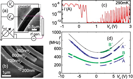
Figure 1. The measurement setup, chip geometry and basic sample characterization. (a) Scanning electron microscope (SEM) image of a typical suspended carbon nanotube, combined with a simplified sketch of the measurement electronics. dc gate and bias voltages are applied and the low-frequency current signal is measured via a preamplifier; in addition, an rf signal can be applied via an antenna hanging several centimeters above the chip. (b) SEM image of the electrode geometry, displaying concentric, ring segment-shaped contact electrodes around a nanotube growth catalyst island. All transport measurements presented here are measured across the same 700 nm wide trench. (c) Measurement of the dc current Idc(Vg) through the nanotube device as a function of back gate voltage Vg for an applied bias Vsd = 0.2 mV . (d) Observed rf-driven mechanical resonance frequencies f(Vg) as a function of back gate voltage Vg; see text for details.
Download figure:
Standard imageElectronic transport measurements were carried out in a 3He evaporation cooling system at T3He = 290 mK and in a dilution refrigerator at Tmc,base = 25 mK. The electronic measurement setup, as sketched in figure 1(a), closely follows [10, 11]. A gate voltage Vg is applied to the substrate as back gate, and a bias voltage Vsd across the device. The resulting dc current through the device is measured via a preamplifier, as required for Coulomb blockade transport spectroscopy [14]. An antenna suspended close to the chip provides a means to apply a radio-frequency (rf) signal contact-free.
First, we characterize the basic electronic and electromechanical properties of the device. As can be seen from the dc current measurement in figure 1(c), our device exhibits the typical electronic behavior of a very clean and regular small band gap nanotube. The measurement displays the dc current Idc as a function of the applied gate voltage Vg, for a low constant dc bias voltage Vsd = 0.2 mV . For Vg < 0.5 V , highly transparent contacts in hole conduction lead to a rapid transition from Coulomb blockade to the Fabry–Perot interference regime [15]. Around Vg ≃ 0.75 V , current is suppressed as the electrochemical potential is located within the semiconducting band gap. For Vg > 1 V , electron conduction becomes visible through sharp, well-defined Coulomb blockade oscillations with the characteristic fourfold pattern of the carbon nanotube level structure [16]. Regular Kondo conductance enhancement [17] emerges for Ne− > 15, again confirming the presence of a defect-free single-wall carbon nanotube.
When an rf signal is applied at mechanical resonance, the nanotube vibrates, leading to a change in detected, time-averaged dc current [10]. This signal can be identified via its characteristic dependence on the back gate voltage Vg: electrostatic forces on the influenced charge on the nanotube lead to mechanical tension, and thereby an increase in resonance frequency of the transversal vibration mode. Figure 1(d) shows a map of such resonance positions, displaying the resonance frequency as a function of back gate voltage Vg. It thus characterizes the basic electromechanical properties of our device. Among several other weaker features, four clear structures, plotted in figure 1(d) and labeled A, B, A' and B', can be seen in the observed frequency range, with the overall gate voltage dependence typical of the mechanical response of a tensioned carbon nanotube resonator [1, 2, 10].
Traces A' and B' coincide over a wide range with double the frequency of traces A and B (plotted in figure 1(d) as thin black lines). It appears unlikely that these represent higher mechanical modes, since in the low tension limit an exact frequency doubling is not expected [18]. Instead, A' and B' can represent different driving mechanisms for the modes of A and B. In the literature, e.g. parametric resonance has been demonstrated in measurements on nanotube resonators [19, 20]. The observation of the two modes A and B is consistent with mechanical motion of two adjacent suspended nanotube segments of different length, as is visible in the chip geometry of figure 1(b). Assuming the minimum resonance frequency close to charge neutrality to be the case of vanishing mechanical tension, the ratio of the minimum frequencies of A and B, fmin,A/fmin,B = 253 MHz/182 MHz ≃ 1.39, agrees very well with the expectation from the different trench widths (ℓB/ℓA)2 = (700 nm/600 nm)2 ≃ 1.36. The detailed mechanism leading to the signal contribution of the second nanotube segment next to the contacted 700 nm gap is still under investigation.
In the following, we return to measurements without any applied rf driving signal. Figure 2(a) displays a lock-in measurement of the differential conductance of the suspended carbon nanotube quantum dot, as a function of gate voltage Vg and bias voltage Vsd. A positive gate voltage is used to tune the quantum dot into the regime with an electron number of 38 ⩽ Ne− ⩽ 42, where it is strongly tunnel-coupled to the contact electrodes. Several features on the plot can be immediately identified and are well understood. The narrow, approximately gate voltage-independent conductance minimum around Vsd = 0 in figure 2(a) is caused by superconductivity of the metallic rhenium leads; two Kondo ridges of enhanced low-bias conductance become clearly visible around Vg = 3.84 V (Ne− = 39) and Vg = 4.0 V (Ne− = 41).
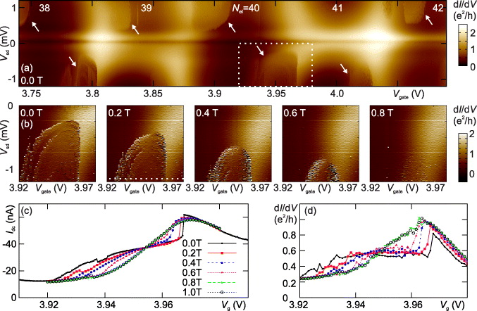
Figure 2. Feedback effects in a non-driven resonator (all measurements at Tmc,base). (a) Differential conductance dI/dVsd(Vg, Vsd) (no rf signal applied; lock-in measurement with an excitation of Vsd,ac = 5 μV rms at 137 Hz) of the carbon nanotube quantum dot at zero magnetic field, displaying fourfold shell filling combined with Kondo effect and traces of superconductivity in the metallic leads (see text). At finite bias, strong switching effects attributable to mechanical self-excitation become visible, indicated by white arrows [11, 21]. (b) Detail of panel (a) for increasing magnetic field, this time plotting the numerical derivative of the simultaneously measured dc current Idc(Vg, Vsd). Already at B = 0.8 T, the self-driving effects are completely suppressed. (c) dc current Idc(Vg) along the trace of constant Vsd = −1.15 mV , as marked in panel (b) with a dotted line; and (d) the corresponding differential conductance dI/dVsd(Vg).
Download figure:
Standard imageIn addition, the differential conductance signal from figure 2(a) exhibits sharply delineated regions of modified signal level, often accompanied by switching behavior, see white arrows in the figure. This has already been observed previously in clean suspended carbon nanotube quantum dots [11]. As predicted in [21, 22] and confirmed in [11], in these parameter regions single-electron tunneling from dc current alone suffices to coherently drive the mechanical motion via a positive feedback mechanism. In turn, this becomes visible in the recorded current or conductance signal as well.
The panels of figure 2(b) display a detail (enlarged) of the parameter region of figure 2(a), this time plotting as differential conductance the numerical derivative of the dc current recorded simultaneously with the lock-in signal. Although this value is affected by a larger noise level, it reproduces more faithfully one-time switching events while sweeping the bias voltage, which delimit the feedback regions. A clear substructure emerges inside the feedback region, which so far has not found any equivalent in theoretical considerations. In addition, when increasing an externally applied magnetic field perpendicular to the chip surface, the parameter regions of positive feedback shrink. As can be seen from the panels of figure 2(b), applying a magnetic field of B = 0.8 T already completely suppresses the self-driving effect within the observed region.
This is further illustrated by the line traces of figures 2(c) and (d), displaying the dc current (panel (c)) and the differential conductance (panel (d)) as a function of gate voltage Vg at constant Vsd = −1.15 mV across the parameter regions of figure 2(b). While no significant changes take place outside the positive feedback region, the discontinuous behavior at zero field becomes smooth, and only slight fluctuations remain at B = 1 T. In particular the current agrees very well with the prediction of [21, 22] in the cases of present and suppressed feedback.
While it has been shown in [11] that large electronic tunnel rates are an important prerequisite for self-excitation, here the conductance remains unchanged outside the feedback-dominated regions. The magnetic field does not significantly influence the electronic tunnel rates, excluding such a mechanism for the suppression of the self-excitation. A second prerequisite is a high mechanical quality factor [21, 22], since the feedback mechanism has to compensate and overcome damping of the mechanical oscillation. Consequently, the suppression of self-driving indicates a magnetic-field-induced additional damping mechanism.
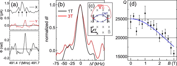
To verify this conclusion from the pure dc measurements, we measure the frequency dependence of the rf-driven resonator response. An additional damping mechanism in a magnetic field should here become visible as a resonance peak broadening, i.e. a decrease in the effective quality factor Q. A constant positive gate voltage Vg = 3.91 V is used to tune the quantum dot into the Coulomb blockade region with electron number Ne− = 40. Because of the transparent tunnel barriers to the leads, significant cotunneling conductance of the order of Gcot ≃ 0.4 e2/h can still be observed in this parameter region, enabling the detection of the mechanical resonance in dc current. Extending the mechanical resonance detection setup of [10, 11] to increase the sensitivity, the applied rf signal is amplitude-modulated at a low frequency fam = 137 Hz, such that the period 1/fam ≃ 7 ms is larger than the oscillation decay timescale ∼Q/f expected from the literature [10]. The corresponding low-frequency modulation of the current signal is recorded by a lock-in amplifier. In addition, we drive at double frequency (A' in figure 1(d)), as this results in a stronger resonance signal.
Figure 3(a) displays a typical resulting in-phase (x), out-of-phase (y) and phase angle (ϕ) amplitude modulation response signal as a function of the driving frequency f. In the in-phase (x) response, a multi-peak structure emerges. Indications of this multi-peak shape (see the arrows in figure 3(a)) remain visible even at the lowermost driving power and suggest a more complex coupling of the rf driving signal into the electromechanical system than only actuation via electrostatic force [10, 19, 20]. As can be seen from both the y response and the phase angle, in spite of the low amplitude modulation frequency, a distinct phase shift of the response on resonance is still visible. The shift of approximately Δϕ = 0.2 rad corresponds to a delay time of Δt = 0.35 ms, of the order of 105 mechanical oscillation cycles. Given that previously observed nanotube resonators [10, 20] have exhibited quality factors of that order of magnitude, this is consistent with mechanical storage of vibration energy and later release within one amplitude modulation cycle, leading to a delayed driving response.
Figure 3. Broadening of the driven mechanical resonance in a magnetic field (all measurements at Tmc,base). (a) Observed mechanical resonance for Vg = 3.91 V and Vsd = 0.3 mV (nominal maximal driving signal after attenuators −42 dBm). The mechanical driving signal is amplitude-modulated at low frequency fam = 137 Hz; the plot displays the lock-in response (upper panel: x, y; lower panel: ϕ) at that frequency of the averaged current through the carbon nanotube quantum dot [10]. (b) Selected mechanical resonance curves (y lock-in signal) for B = 1 T and B = 3 T (nominal maximal driving signal −41 dBm). At the higher magnetic field, a slightly broader resonance can be observed. (c) Circuit model of electromechanical damping by Ohmic dissipation, see text. (d) Quality factor Q of the resonance extracted from multiple traces as in panel (b), as a function of magnetic field. The solid line provides a model fit, assuming both a magnetic-field-induced and a magnetic-field-independent damping contribution (see text).
Download figure:
Standard image
To avoid fitting of the multi-peak structure in the in-phase (x) signal, we focus in the following on the out-of-phase (y) signal induced by the phase shift. Figure 3(b) shows selected frequency response traces of the mechanical resonance, recorded at an external magnetic field of B = 1 T and B = 3 T, respectively, and pointing towards a slight broadening of the peak structure at higher magnetic field. Evaluation of many similar curves, including repeated measurements at the same magnetic field value and over a large driving power range, leads to the plot of figure 3(d). Here, the width of the resonance peaks is plotted in terms of an experimentally observed quality factor Q as a function of the magnetic field B. Indeed, the measured peak width increases (and Q decreases) significantly above B = 1 T.
A straightforward circuit model sketched in figure 3(c) can be used to describe the magnetic field dependence. A vibration component perpendicular to the magnetic field leads to an induced ac voltage across the resonator. We assume the carbon nanotube resonator to be partially electrically shortened in the rf signal frequency range via an Ohmic resistance R and a large parasitic capacitance. For simplicity, we do not take into account the deflection shape but assume a uniform beam deflection along the entire nanotube of length L and mass m to estimate the magnetic flux modulation. As a result, eddy currents lead to a damping of the mechanical motion corresponding to

as both the induced voltage and the resulting eddy current are proportional to B. Assuming an additional magnetic-field-independent resonator damping, which determines the zero external field quality factor Q0, we obtain the expression

The solid line in figure 3(d) provides a best fit of this function to the data, using Q0 and q as free parameters and resulting in the values q = 5.381 × 10⁵ T2 and Q0 = 25 020. As is visible in figure 3 this model describes our measurement results well. This thereby confirms the presence of a magnetic-field-induced damping mechanism. Using the resonance frequency f and estimating L ≃ 700 nm and m ≃ 1.3 × 10⁻²¹ kg, we obtain a value for the Ohmic resistance of R ≃ 200 kΩ in the replacement circuit of figure 3(c).
As a last remark, using the fit function of figure 3(d) one obtains Q(0.8 T)/Q(0 T) ≃ 0.97, i.e. only a very small decrease of the effective quality factor within the magnetic field range covered in figure 2. A likely reason for this is that the resonance peak widths evaluated in figure 3(d) do not solely correspond to the device quality factor entering the self-excitation, but are broadened by additional mechanisms, leading to an underestimation of the low-field quality factor Q0.
Summarizing, we characterize a quantum dot in a suspended ultra-clean single-wall carbon nanotube, which also acts as a nano-electromechanical resonator. We observe how feedback and self-driving effects, where only dc current is sufficient to drive resonator motion, are suppressed in a finite magnetic field. The conclusion that the magnetic field induces an additional damping mechanism is confirmed by tracing the driven resonator response as a function of magnetic field. We modelled the decrease of the mechanical quality factor successfully using eddy current damping.
Acknowledgments
The authors thank the Deutsche Forschungsgemeinschaft (Emmy Noether grant Hu 1808/1-1, SFB 631 TP A11 and GRK 1570) and the Studienstiftung des deutschen Volkes for financial support.