


Abstract
The nitrogen-vacancy colour centre in diamond is emerging as one of the most important solid-state quantum systems. It has applications to fields including high-precision sensing, quantum computing, single photon communication, metrology, nanoscale magnetic imaging and biosensing. For all of these applications, a high quantum yield of emitted photons is desirable. However, diamond samples engineered to have high densities of nitrogen-vacancy centres show levels of brightness varying significantly within single batches, or even within the same sample. Here we show that nearby nitrogen impurities quench emission of nitrogen-vacancy centres via non-radiative transitions, resulting in a reduced fluorescence quantum yield. We monitored the emission properties of nitrogen-vacancy centre ensembles from synthetic diamond samples with different concentrations of nitrogen impurities. All samples were irradiated with high energy electrons to create high densities of nitrogen-vacancy centres relative to the concentration of nitrogen impurities. While at low nitrogen densities of 1.81 ppm we measured a lifetime of 13.9 ns, we observed a strong reduction in lifetime with increasing nitrogen density. We measure a lifetime as low as 4.4 ns at a nitrogen density of 380 ppm. The change in lifetime matches a reduction in relative fluorescence quantum yield from 77.4% to 32% with an increase in nitrogen density from 88 ppm to 380 ppm, respectively. These results will inform the conditions required to optimise the properties of diamond crystals devices based on the fluorescence of nitrogen-vacancy centres. Furthermore, this work provides insights into the origin of inhomogeneities observed in high-density nitrogen-vacancy ensembles within diamonds and nanodiamonds.
Export citation and abstract BibTeX RIS

Original content from this work may be used under the terms of the Creative Commons Attribution 4.0 licence. Any further distribution of this work must maintain attribution to the author(s) and the title of the work, journal citation and DOI.
1. Introduction
The nitrogen-vacancy (NV) centre in diamond is a fluorescent defect consisting of a nitrogen atom neighbouring a vacancy, or missing carbon atom, in the diamond lattice [1]. The negatively charged NV centre (or NV−) in diamond has already demonstrated numerous applications [2], for example as a photostable emitter for biolabeling with nanodiamonds [3–5], or nanoscale sensor of temperature, magnetic and electric fields [6–11]. These applications take advantage of the NV− high sensing and imaging spatial resolution, as well as operation under ambient conditions.
A key factor in many applications of the NV− centre, especially when using an ensemble of defects, is the emission intensity of the sample. As a first approximation, the emission intensity is proportional to the density of NV− centres, i.e. proportional to the number of emitters. Because of this proportionality, multiple studies investigated methods to improve the creation efficiency of NV− centres in diamond and nanodiamonds [12–16]. However, the fluorescence quantum yield of the NV− centre is commonly thought to be constant and therefore it is not included in the discussion. Despite this, recent studies suggest that the presence of nitrogen defects, as well as other defects, reduces the emission intensity of the NV− centres [17–19].
Single substitutional nitrogen defects (Ns) are ubiquitous in diamond samples with high densities of NV centres therefore, they are of particular relevance in the study of the NV− centre fluorescence. While only the NV− centre has a spin-dependent emission intensity used for quantum sensing applications, the presence of neutrally charged states (NV0) contribute to background fluorescence, reducing signal to noise. To maintain a negatively charged state, the NV centre requires an electron donor within the diamond crystal. Nitrogen defects, especially the neutrally charged Ns 0 defects, can donate their electron to the NV centre [20, 21]. This process creates pairs of N+–NV− in the diamond, as discussed in the literature [17].
In this study, we show that the fluorescence quantum yield of the NV− centres drop with increasing concentration of Ns 0 defects. We investigated a series of HPHT and CVD (chemical vapour deposition) diamond samples whose nitrogen concentrations ranged from 2 ppm up to almost 400 ppm. We characterised the photodynamics—such as emission intensity, lifetime and fluorescence quantum yield—for each sample and as a function of Ns 0 concentration. We attribute the change in lifetime and fluorescence quantum yield to the non-radiative tunnelling of the electron within the pair N+–NV− while the NV− is in the excited state. Finally, we establish a model curve to predict the change in fluorescence quantum yield from the Ns 0 concentration.
The fluorescence quantum yield is defined as the fraction of photons emitted compared to the number of photons absorbed from the excitation source [22]. In a simple two-level system, the emitter reaches its excited state when it absorbs a photon. The emitter will then return to its ground state producing a photon. In this example, the system has 100% fluorescence quantum yield: for each photon absorbed, a photon is emitted. However, in more complex systems, such as the NV− centre in our study, the relaxation process may involve non-radiative decay pathways, which results in the decrease of the system's fluorescence quantum yield. As an example, the transition from the NV− excited state ms = ±1 spin projection to its singlet state is the most well-known non-radiative decay pathway of the NV− centre. The presence of the non-radiative transition to the singlet state—initially observed as a lifetime reduction of the NV− ms = ±1 excited state—causes the different spin states of the NV− centre to have different fluorescence quantum yield [23]. Using the emission intensity to distinguish between spin states is the fundamental key that allows most quantum sensing applications with the NV− centre.
However, an overall spin-independent low fluorescence quantum yield has a negative impact on multiple applications of the NV− centres in diamond. For example, a low fluorescence quantum yield hinders the use of nanodiamonds as fluorescent biolabels. NV-containing nanodiamonds already show low brightness per unit mass compared to other biolabels [24]. A further reduction in the nanodiamonds emission intensity, due to the low fluorescence quantum yield, disrupts their viability in bioimaging applications, despite their strong photostability. Additionally, a reduced fluorescence quantum yield has a two-fold impact on applications of the NV− centres in the field of optical sensing. Firstly, the decrease in emission intensity signal reduces the signal to noise ratio—limited by the photon shot noise—of any sensing measurement. Secondly, the non-radiative decay pathway reduces the intensity contrast between the two spin-based emission intensities of the NV− centres, further decreasing the sensitivity of the system [18].
Previous studies have reported the fluorescence quantum yield of 82% for shallow implanted NV− centre in single-crystal diamond [25]. However, NV− centres close to the surface of the diamond sample show a reduced fluorescence quantum yield attributed to the dipole interaction with surface defects and group functionalisation [25, 26]. Other studies focus on the reduction of quantum yield caused by irradiation damage in the diamond lattice [19]. Additionally, few studies already observed a change in the emission properties of the NV centres caused by nitrogen defects within the crystal [17, 18]. As aforementioned, the relationship between the NV− centre and nitrogen defects is particularly important due to the prevalence of single nitrogen defects in commonly used diamond samples, such as those created by high-pressure high-temperature (HPHT) synthesis.
HPHT diamond samples are commonly used as starting material for the creation of nanodiamond particles as well as the production of diamond chips with high-density ensembles of NV− centres. However, the HPHT synthesis method naturally incorporates single substitutional nitrogen defects (Ns 0) at different concentrations within the same crystal. The difference in nitrogen concentration comes from the presence of growth sectors in each sample [27, 28]. The growth sectors arise from the HPHT synthesis, during which the diamond crystal grows along different growth faces starting from a common seed. The growth faces incorporate defects at different rates and become growth sectors distinguishable by their defect concentrations. In particular, it is typical for the Ns 0 concentration to range from 50 ppm up to 400 ppm within different growth sectors in HPHT diamonds. The relatively high concentration of single substitutional nitrogen defects in HPHT diamonds facilitates the creation of high density of NV centres and helps maintain the NV centres in their negatively charged state. However, a low percentage of Ns 0 defects are converted into NV centres, and many forms of nitrogen-based defects remain in the crystal lattice after processing. While the interactions between Ns 0 defects and the NV− centres have been studied mainly with reference to the change in spin coherence time [29], we focus on the direct effect of the remaining Ns 0 defects on the fluorescence of the NV− centre.
2. Instruments and methods
We used single-crystal synthetic diamonds to demonstrate the effect of nitrogen defects on the emission of the NV− centre. We subdivided our diamonds in three distinct batches based on their synthesis process and irradiation parameters. Table 1 summarises the batches we used in this study and their characteristics. The HPHT diamonds in batch 2 showed growth sectors with different defect concentrations, as discussed above (the growth sectors are visible in the micrographs reported in figure S1 of the supp. info (https://stacks.iop.org/NJP/24/033053/mmedia)). Each growth sector within a single HPHT sample shows very distinct optical properties and therefore, we included the different sectors as separate data points.
Table 1. Summary of the samples and sectors investigated with associated supplier, diamond type, NV centre creation processing and further details associated with each set. Batch 1 has two CVD-grown samples (type IIa) irradiated at relatively low fluences and used as a benchmark for low-nitrogen behaviour. Batch 2 has two HPHT samples (type Ib), each having multiple growth sectors characterised by different nitrogen concentrations (see figure S1 in the supp. info). Batch 3 includes four HPHT samples (type Ib) irradiated at different fluences to create different NV centre concentrations starting from samples with similar nitrogen concentrations.
| Supplier | Diamond type | Processing | Additional details | |
|---|---|---|---|---|
| Batch 1 | Fraunhofer IAF | CVD IIa | 2 × 1017 cm−2 electron irradiation 1000 °C annealing for 2 h | 2 samples |
| Batch 2 | ElementSix | HPHT Ib | 1018 cm−2 electron irradiation 900 °C annealing for 2 h | 2 samples: 3 growth |
| sectors each | ||||
| Batch 3 | Sumitomo Electric | HPHT Ib | 0.5–5 × 1018 cm−2 electron irradiation 1000 °C annealing for 2 h | 4 samples |
Batch 1 includes two CVD samples grown at the Fraunhofer IAF, Freiburg. Nitrogen defects were incorporated during the synthesis process of both samples under similar growth conditions. The samples were irradiated with a 2 MeV electron beam to a total fluence of 2 × 1017 cm−2 at the National Institutes for Quantum Science and Technology (QST), Takasaki, Japan. The samples were annealed at 1000 °C for 2 h to create the NV centres [14, 30]. We used the sample in batch 1 as a benchmark for the behaviour of an ensemble of NV− centres with low concentrations of Ns 0 defects (<2 ppm). Batch 2 is characterised by samples with different nitrogen concentrations but processed using the same total electron fluence. It includes two HPHT Ib samples from ElementSix. Both samples show the growth sectors caused by HPHT synthesis, as discussed in the introduction. The supplementary information shows micrographs of the samples and their growth sectors visible in transmission under white-light illumination (see figure S1). The samples were irradiated in the same 2 MeV electron beam facility at QST, to a total fluence of 1 × 1018 cm−2 and annealed afterwards at 900 °C for 2 h. We selected three distinct sectors from each sample for a total of six investigated nitrogen concentrations. Finally, as part of batch 3, we irradiated four more HPHT Ib samples to different total electron fluences. The samples in batch 3 were cut from a few larger HPHT samples from Sumitomo Electric before processing. The cut samples do not show inhomogeneity from different growth sectors, except for a small corner in the 1 × 1018 cm−2 irradiated sample (see figure S1). Batch 3 samples were irradiated with 2 MeV electrons at QST, however, the total irradiation fluence reached was different for each sample. The samples were part of a series of growing fluences starting from 0.5 × 1018 cm−2, then 1 × 1018 cm−2, 2 × 1018 cm−2 and finally 5 × 1018 cm−2. All samples in batch 3 were annealed at 1000 °C for 2 h. Batch 3 allowed us to verify that our observations do not change with varying NV concentration in the sample and, instead, are predominantly linked to the concentration of Ns 0 defects.
Initially, we characterised the samples by visible and infrared absorption spectroscopy to determine the concentration of NV− centres and nitrogen defects, respectively. We performed visible absorption spectroscopy using a CRAIC Apollo 785 Raman micro-spectrophotometer. The instrument allowed us to measure the absorption signal in transmission from an area of 20 × 20 μm2 in size. We repeated the absorption measurement three times in different areas within the same sample and growth sector. We used the different areas to calculate the uncertainty in our defects characterisation within each sample and sector. When investigating different sectors, we recorded the measurements in areas far away from the edge between sectors to avoid possible inhomogeneity across the samples' depth. We collected the infrared absorption spectra (FTIR spectroscopy) using a PerkinElmer Spotlight 400. We measured the infrared absorption signal from an area 50 × 50 μm2 in size and, as before, we recorded three different spectra from each sample/growth sector. The range of wavenumbers in our infrared absorption spectra includes the signatures of different nitrogen-based defects in diamond. We calculated numerically the concentration of Ns 0 defects and discussed only qualitatively the presence (or absence) of the other defects in the next paragraph. For both NV− and Ns 0 estimation, we averaged the results between the three areas and used the maximum semi-dispersion of the calculated values as the uncertainty of the result. The suppl. information includes examples of both the visible and infrared absorption spectra (figure S3), together with the exact processing and calculation we used to determine the different concentrations in the samples.
It is important to discuss the charge states of the defects we observed. The estimation of the NV− concentration is based on the absorption coefficient of the sample at 532 nm [31]. Since the absorption spectra show no trace of the NV0 charge state and the light intensity is not strong enough to ionize the NV− centre, we can assume that the entirety of the absorption comes from the negatively charged NV centre (NV−). Further analysis of the emission spectra from the samples supports our assumption. Nonetheless, all values of NV− concentration we report are upper bounds. When discussing nitrogen defects, we only refer to the neutral substitutional single nitrogen defect—or Ns 0 defect—commonly found in HPHT Ib diamond crystal [32]. The Ns 0 defect is also known in the literature as P1 centre (in electron paramagnetic resonance spectroscopy) or C centre (in infrared spectroscopy). The spectral window used to calculate the concentration of Ns 0 defects allows us to discuss the presence of positively charged single nitrogen defects (Ns +) [33] and the double substitutional nitrogen defect (known as A centre in infrared spectroscopy) [34]. Our samples show no measurable presence of double substitutional nitrogen, and the Ns + defect is primarily hidden by the strong absorption of the Ns 0 defect in the wide wavenumber range 1050–1350 cm−1 (see figure S2 in the suppl. information). The Ns + defect starts to be identifiable as a peak at 1332 cm−1 only on the sample with the largest NV concentration and low Ns 0 density. Additionally, we exclude other possible charge states for the single substitutional nitrogen, such as the negative charge state (Ns −) and the double-positive charge states (Ns ++), since both of them are shown to be unstable under standard experimental conditions [35].
Finally, the defect concentrations in the CVD samples were determined using different methods. Since the FTIR measurement is not sensitive enough to detect low nitrogen concentrations, we measured the UV-visible absorption spectra of the sample and calculated the concentration of Ns 0 defects from their UV absorption band [36]. Similarly, the visible absorption measurement is not able to detect low NV− concentration, so we determined the NV− concentration from the emission intensity of the sample. We compared the emission intensity of the samples with unknown NV− concentration to the emission intensity of a reference sample, using the same optical system. We measured the NV− concentration of the reference sample using visible absorption spectroscopy as mentioned in the paragraph above. We want to highlight here that this last approach, by our own conclusions discussed further in the paper, is not always reliable and depends on the relative density of Ns 0 defects between the unknown and reference samples.
We characterised the emission properties of the samples with a custom-built fluorescence confocal microscope. The samples were excited with a picosecond-pulsed tuneable laser (Fianium whitelase supercontinuum, NKT Photonics). The excitation light spread over a 10 nm band centred at 520 nm at a repetition rate of 10 MHz. A 0.9 NA microscope objective (Plan Apo EPI, Nikon) focussed the excitation on the sample as well as collecting the emission from the NV centres. We filtered the emission with a 532 nm long-pass filter to remove the excitation source and with an additional 725 nm long-pass filter to reduce to a minimum the collection of emission from the neutral charge state of the NV centre (NV0). A more detailed study reported in the suppl. information shows that the NV0 contribution in our signal was always less than 0.3% (figure S6). We fibre-coupled the filtered emission towards an avalanche photodiode detector (APD, AQRH-XX-TR, Excelitas). The intensity signal was sent to a time-tagging correlation card (TimeHarp 260, PicoQuant) for the lifetime measurement. The strength of the emission intensity over time (fluorescence timetrace) was recorded simultaneously with the lifetime measurement, using the open-source QuDi software [37]. We measured both the fluorescence timetrace and the lifetime as a function of excitation power. Example trends are reported in figure S7 of the suppl. information. As we did for the absorption measurements, we collected the timetrace and lifetime curves in three separate areas within each sample and growth sector. The uncertainties in our data reflect the differences between such areas inside a single sample/sector.
3. Results and discussion
Figure 1(a) shows the distribution of Ns 0 defects and NV− centre concentration for the samples included in this study. The different batches result in three areas in the scatter plot: (a) in the bottom left corner of the plot we have the CVD-grown samples from batch 1, which overlap due to their very similar growth parameters. The plot shows they have both low Ns 0 and NV− concentration. (b) A series of points positioned along a horizontal line corresponding to an NV− centre concentration of ∼1 ppm (highlighted in figure 1(a) by a shaded band). In this area we have the HPHT samples irradiated at a fluence of 1018 cm−2. At a fluence of 1018 cm−2, the concentration of nitrogen impurities in HPHT-synthesised diamond crystals (in the order of 50–400 ppm) is much higher than the density of created vacancies—estimated to be around 10 ppm immediately after irradiation [38]. Therefore, in these samples, the NV concentration is limited by the number of vacancies introduced by the irradiation process. (c) A downward diagonal line, from the top of the plot to its bottom, intersects the 1 ppm horizontal line. This area corresponds to the samples irradiated at different fluences. Starting from the highest point (with an NV− density of 4.13 ± 0.08 ppm) which represents the sample irradiated at a fluence of 5 × 1018 cm−2, down to the lowest point of 0.21 ± 0.02 ppm of NV− centres (but with nitrogen concentration of 173 ± 3 ppm) which represents the sample irradiated at a fluence of 0.5 × 1018 cm−2.
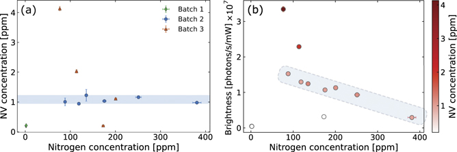
Figure 1. (a) Concentration of NV− centres and Ns 0 defects for all investigated samples and sectors. The data points are grouped in three batches by colour and shape. The green (diamond) data show the CVD samples from batch 1, which overlap due to their similar growth parameters. Blue (circles) data show the results from the multiple sectors within the HPHT samples in batch 2. All sectors in batch 2 were irradiated to the same total fluence, therefore showing similar concentrations of NV centres. The orange (triangles) data from batch 3 show four different HPHT samples processed with different electron irradiation fluences. The different total fluences cause the creation of varying densities of NV centres, with the highest fluence of 5 × 1018 cm−2 corresponding to the sample with more than 4 ppm of NV centres. (b) Brightness distribution of the investigated samples as a function of Ns 0 (on the x-axis) and NV− concentration (on the colour axis). The brightness is calculated as the rate at which the emission increases with increasing excitation power (see the suppl. information for more details). The brightness changes with the NV− concentration (represented by the different shades of red), with darker spots corresponding to higher NV− concentrations. The blue shaded areas in both plots highlight the samples irradiated to the same total fluence (1 × 1018 cm−2). In (a) the highlighted samples show a similar NV− concentration (0.944–1.23 ppm) due to the constant irradiation fluence. In (b) the highlighted points show a drop in brightness with increasing nitrogen concentration, even if the NV− concentration remains approximately constant.
Download figure:
Standard image High-resolution imageFigure 1(b) shows how the samples' brightness changes with Ns 0 and NV− centre concentration. We calculated the brightness as the rate at which the emission intensity increased with excitation power (see figure S7 in the suppl. information). The NV− concentration in figure 1(b) is expressed via colorscale, from low NV− concentration in white to high NV− concentration in dark red (or dark grey in grayscale). A direct comparison between the plots in figure 1 reveals two main points of discussion:
- (a)Considering only the samples at the highest and lowest concentrations of NV− centres (outside the shaded blue areas in both plots) the brightness of the sample directly correlates to the NV− concentration. This result matches our hypothesis. A high concentration of NV− centres corresponds to more NV− centres being excited and thus emitting in the confocal volume of our microscope, which in turn, corresponds to high emission intensity at a fixed excitation intensity. The reverse is true for low concentrations of NV− centres.
- (b)The samples with a comparable NV− concentration in figure 1(a) did not show a similar brightness value in figure 1(b). These data points are highlighted in both plots by a shaded blue area. The samples with comparable NV− centre concentration demonstrate a drop of the brightness with increasing concentration of Ns 0 defects. The brightness drops by more than a factor of 5 when the nitrogen concentration changes from 88 ± 2 ppm to 380 ± 10 ppm.
Since the drop in brightness cannot be explained by the presence of fewer emitters, we investigated the possible decay pathways from the excited state of the NV− centre using lifetime measurements. We performed lifetime measurements on all samples to understand how the decay rates depend on the concentration of Ns 0 defects. The measured lifetime corresponds to the inverse of the sum of all decay rates from the excited state of the NV− centre:

We distinguish between three possible decay rates: krad is the radiative rate corresponding with the emission of photons; ktunnel is the non-radiative tunnelling rate within the NV−–N+ pair, which depends on the distance between the NV− centre and its closest Ns 0 defect; knon-rad is any other source of non-radiative decay independent of the nitrogen concentration, such as the transition to the NV− singlet state.
To calculate the average lifetime of each measurement, we fit a stretched exponential to the experimental data (see figure S8 of the suppl. information). Since all our measurements are performed on an ensemble of NV− centres, we expect to measure a distribution of different decay rates [39]. A stretched exponential takes the form of: ![${I}_{0}\,\mathrm{exp}\left[-{\left(t/{\tau }_{0}\right)}^{\beta }\right]$](https://content.cld.iop.org/journals/1367-2630/24/3/033053/revision2/njpac5ca9ieqn1.gif) . τ0 represents the time at which the intensity drops by a factor e independently of the parameter β, and β is the dispersion parameter in the range 0 < β ⩽ 1 that indicates the deviation of the curve from a single exponential (corresponding to β = 1). β < 1 corresponds to a wide distribution of lifetimes, with the smaller values of β indicating a more spread lifetime distribution. However, τ0 and β do not directly represent the physical parameters of the decaying system [39]. Nonetheless, the fit parameters τ0 and β can be used to calculate the average value of the distribution of lifetimes
. τ0 represents the time at which the intensity drops by a factor e independently of the parameter β, and β is the dispersion parameter in the range 0 < β ⩽ 1 that indicates the deviation of the curve from a single exponential (corresponding to β = 1). β < 1 corresponds to a wide distribution of lifetimes, with the smaller values of β indicating a more spread lifetime distribution. However, τ0 and β do not directly represent the physical parameters of the decaying system [39]. Nonetheless, the fit parameters τ0 and β can be used to calculate the average value of the distribution of lifetimes  of the ensemble of NV− centres (see the suppl. information for the calculation).
We calculated the average fluorescence lifetime for each excitation power. As the excitation power increased, the lifetime plateau towards a constant value. Some examples of the stretched exponential parameters and average lifetimes with excitation power are reported in the suppl. information (figures S9 and S10). We associated each sample with the average lifetime calculated at ∼50 μW (∼73 kW/cm2), which was the point at which the plateau started. Figure 2 shows that average fluorescence lifetime decreases with increasing Ns 0 concentration for all the samples studied in this work. It is important to note that the decreasing trend is independent of the NV− concentration, and only follows the calculated Ns 0 concentration. The independence from the NV− concentration is highlighted by the data point from batch 3 (orange triangles in figure 2). Due to the variation of electron dose used during irradiation, the samples in batch 3 display NV− concentrations that range between four times and one-fifth of the average concentration in batch 2 (blue circles in figure 2). Despite the strong difference in NV− concentrations, the trend and values of the calculated average lifetimes do not deviate significantly between the samples of batch 2 and batch 3.
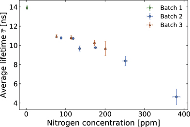
Figure 2. Average fluorescence lifetimes measured from the samples and sectors studied as a function of nitrogen (Ns 0) concentration. The scatter plot shows a decrease in the average lifetime with increasing nitrogen concentration.
Download figure:
Standard image High-resolution imageAs shown from equation (1), the observed decrease in the average fluorescence lifetime with Ns 0 concentration is explained by the increase of either the radiative rate or the tunnelling rate (or a combination of both). However, an increase in the radiative emission rate would have matched an increase in brightness. We, therefore, attribute the observed decrease in brightness with Ns 0 concentration to an increased tunnelling rate. The presence of a nitrogen-dependent non-radiative tunnelling rate matches the current scientific literature, and specifically, the work in [17].
The model proposed in [17] is schematically represented in figure 3(a) and can be briefly described as follows: the negatively charged NV− centre is created by a single nitrogen defect donating its free electron and creating an NV−–N+ pair. However, the donated electron can tunnel back to the nitrogen donor transforming the NV− into an NV0. The NV0 will rapidly accept an electron from another (or the same) single nitrogen defect, returning to its NV− state [40]. This latter mechanism also depends on the concentration of Ns 0 defects [41], and prevents us from studying the tunnelling effect through the emission of the NV0 centre. We reported further details on the decrease in NV0 emission with Ns 0 concentration in the suppl. information (figures S4 and S6). The entire tunnelling process will result in the relaxation of the NV− to its ground state without the emission of a photon.
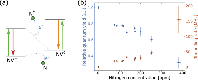
Figure 3. (a) Schematic of the electron tunnelling between NV centres and nitrogen impurities in the diamond. The solid arrows represent the excitation/emission transitions of the NV centre charge states. The blue curved dashed arrows figuratively indicate the tunnelling of the additional electron to and from the closest nitrogen impurity (represented by the spheres on the edges of the schematic). The grey dashed lines show the equivalent non-radiative transitions between the charge state, which causes the reduced measured lifetime. (b) Relative fluorescence quantum yield (blue dots) and tunnelling rate (orange triangles) calculated from the lifetime measurements as a function of nitrogen concentration. As the nitrogen concentration increases, and hence the average distance between the NV− centres and their closest nitrogen impurity decreases, the tunnelling rate increases. The increase in the non-radiative tunnelling rate corresponds to a decrease in fluorescence quantum yield.
Download figure:
Standard image High-resolution imageFrom theoretical quantum mechanics, the probability of tunnelling increases exponentially with decreasing distance between donor and acceptor. In this work, the average distance between the NV− centre and its closest Ns
0 defect represents the distance between donor and acceptor, and it decreases when the density of single nitrogen defects increases. We extracted the tunnelling rate from equation (1), using the calculated average fluorescence lifetime and assuming constant rates for krad and knon-rad. We used the measured lifetime at the lowest Ns
0 concentration (1.81 ± 0.01 ppm) in batch 1 to calculate the constant sum of krad and knon-rad. The decay rate at 1.81 ppm, further referred to as k0, was k0 = 72.0 ± 0.4 MHz which corresponds to a lifetime of  = 13.90 ± 0.08 ns. Figure 3(b) shows the calculated tunnelling rate ktunnel as a function of Ns
0 concentration in each sample (orange triangles).
= 13.90 ± 0.08 ns. Figure 3(b) shows the calculated tunnelling rate ktunnel as a function of Ns
0 concentration in each sample (orange triangles).
The presence of any non-radiative decay acts to reduce the fluorescence quantum yield of the emitter, the NV− centre. Although we assume there is no tunnelling at the lowest Ns 0 concentration, there are still nitrogen-independent non-radiative rates that decrease the quantum yield below 100%. We define the relative fluorescence quantum yield ɛrel as the ratio between the NV− centre quantum yield and the quantum yield at the lowest Ns 0 concentration (ɛ0). Figure 3(b) shows the relative quantum yield (blue circles) of the samples as a function of their Ns 0 concentration, calculated from the relationship in equation (2).

We observe the highest relative quantum yield of 77.4% with ∼88 ppm of Ns 0 defects. However, the relative quantum yield drops to 32%—less than 1 photon emitted every 3 photons absorbed—with ∼380 ppm of Ns 0 defects.
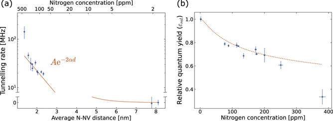
Furthermore, we calculated the average distance between an NV− centre and its closest Ns defect from the measured Ns 0 concentration using the probability distribution reported in the literature [42]. We used the average distance together with the calculated tunnelling rate to identify the exponential decay expected from theory. Figure 4(a) shows the calculated rates (blue data) with the fitted exponential decay (orange solid line). We run a weighted least-squares minimization method to fit the data, using the inverse square of the data uncertainties as weights. We obtained a maximum tunnelling rate, in the limit of zero-distance, A = 185 ± 87 MHz and a decay constant α = 0.53 ± 0.12 nm−1.
Figure 4. (a) Tunnelling rate as a function of the average distance between an NV centre and its closest single nitrogen defect. The orange solid curve shows the exponential decay fit to the experimental data (blue dots). (b) Relative fluorescence quantum yield data (blue dots) overlayed with the theoretical relative fluorescence quantum yield (dashed orange curve) calculated using the parameters obtained from fitting the data in (a).
Download figure:
Standard image High-resolution image
Under the assumption that tunnelling to the closest Ns 0 defect is the only, or the predominant, non-radiative mechanism as a function of Ns 0 defects, we can write a final equation that links the NV− centre relative fluorescence quantum yield (ɛrel) to the Ns 0 concentration (ρN, expressed in nm−3) in the diamond sample.

In equation (3), k0 = 72.0 ± 0.4 MHz is the radiative rate we measured from the low-nitrogen data points, A = 185 ± 87 MHz is the same zero-distance tunnelling rate obtained by fitting the tunnelling rate data in figure 4(a), and  0.294 ± 0.065 nm−1 combines the exponential decay constant α and the constant factor that converts the Ns
0 concentration (expressed in nm−3) in average N–NV distance. The latter constant includes the gamma function Γ(x) which emerges by averaging the possible distances between the NV− centres and their closest Ns
0 defect, given a constant concentration of Ns
0 defects. The calculation is based on the distribution of distances reported in the literature [42]. Figure 4(b) shows how the curve corresponding to equation (3) follows the experimental data (blue dots). According to the curve in figure 4(b), Ns
0 concentrations below 35.5 ppm (6.2 × 10⁻³ nm−3) are required to maintain a relative fluorescence quantum yield above 90%.
0.294 ± 0.065 nm−1 combines the exponential decay constant α and the constant factor that converts the Ns
0 concentration (expressed in nm−3) in average N–NV distance. The latter constant includes the gamma function Γ(x) which emerges by averaging the possible distances between the NV− centres and their closest Ns
0 defect, given a constant concentration of Ns
0 defects. The calculation is based on the distribution of distances reported in the literature [42]. Figure 4(b) shows how the curve corresponding to equation (3) follows the experimental data (blue dots). According to the curve in figure 4(b), Ns
0 concentrations below 35.5 ppm (6.2 × 10⁻³ nm−3) are required to maintain a relative fluorescence quantum yield above 90%.
However, the fluorescence quantum yield is only one of the multiple factors that impact the applications of NV centres. Future works will combine our results with the known effects of the Ns 0 defect, such as the decrease in spin coherence time [29] and the balance between negative and neutral NV charge states [20, 21].
4. Conclusions
We demonstrated the effect of neutral single substitutional nitrogen (Ns 0) defects on the fluorescence quantum yield of NV− centres. Ns 0 defects are the predominant defects in many HPHT single-crystal diamonds commonly used for sensing applications with ensembles of NV− centres. We report the relative fluorescence quantum yield of the NV− centre to be 77.4 ± 0.9% in HPHT diamond samples with 88 ± 2 ppm of Ns 0 defects, the lowest density we investigated in HPHT diamonds. The relative fluorescence quantum yield drops to 32 ± 7% in nitrogen-dense (380 ± 10 ppm) diamond samples. The drop of fluorescence quantum yield with Ns 0 concentration is explained by the tunnelling of electrons within the N+–NV− pair, as previously introduced in the literature. According to our best-fit model, to maintain a relative fluorescence quantum yield above 90% the concentration of Ns 0 defects must be limited to less than 35.5 ppm. These figures are valuable for the development of the ideal diamond materials for light-based sensing applications with the NV− centre: from diamond chips created with high-density ensembles of NV− centres, to bright nanodiamonds observable under commercial microscopes. Finally, our results emphasize the relevance of nitrogen-doped CVD-grown diamonds with a defined concentration of Ns 0 defects. Diamond samples created by HPHT methods, which have often been regarded as a good starting material to create ensembles of NV− centres, show strong variability in the concentration of Ns 0 defects. The variability of Ns 0 defects is attributed to growth sectors (as demonstrated by batch 2 in this study) and impacts the performance of NV− sensing applications, such as inhomogeneity in single-crystal diamond chips and non-uniform emission properties of nanodiamonds.
Acknowledgments
This work was performed in part at the RMIT Micro Nano Research Facility (MNRF) in the Victorian Node of the Australian National Fabrication Facility (ANFF). We acknowledge the Analytical Chemistry Team, Technical Service, STEM College at RMIT University for the support in collecting the FTIR measurements. The authors want to acknowledge the support of Dr Brian Yang from the Australian Research Council (ARC) Centre of Excellence for Nanoscale BioPhotonics laboratories at RMIT University and Dr Neil Manson from the Research School of Physics and Engineering (Australian National University, Canberra) for the useful discussion. MC, BCG and ADG acknowledge funding from the Asian Office of Aerospace Research and Development (AOARD, Funding FA2386-18-1-4056). JJ acknowledges funding from the German federal ministry for education and research, Bundesministerium für Bildung und Forschung (BMBF) under Grant No. 13XP5063. PR acknowledges support through an ARC DECRA Fellowship (Grant No. DE200100279) and a RMIT University Vice-Chancellor's Research Fellowship. ADG and BCG acknowledge financial support from the ARC (FT160100357, CE140100003). This work was in part carried out within the framework of QST Internal Research Initiative and the MEXT Quantum Leap Flagship Program (MEXT Q-LEAP, Grant Number JPMXS0118067395).
Data availability statement
The data generated and/or analysed during the current study are not publicly available for legal/ethical reasons but are available from the corresponding author on reasonable request.