
Abstract
Producing and manipulating graphene on fab-compatible scale, while maintaining its remarkable carrier mobility, is key to finalize its technological application. We show that a large-scale approach (chemical vapor deposition on Cu followed by polymer-mediated semi-dry transfer) yields single-layer graphene crystals fully comparable, in terms of electronic transport, to micro-mechanically exfoliated flakes. Hexagonal boron nitride is used to encapsulate the graphene crystals—without taking part to their detachment from the growth catalyst—and study their intrinsic properties in field-effect devices. At room temperature, the electron-phonon coupling sets the mobility to ∼ 1.3 × 105 cm2 V−1 s−1 at ∼ 1011 cm−2 concentration. At T = 4.2 K, the mobility (>6 × 105 cm2 V−1 s−1 at ∼ 1011 cm−2) is limited by the devices' physical edges, and charge fluctuations < 7 × 109 cm−2 are detected. Under perpendicular magnetic fields, we observe early onset of Landau quantization (B ∼ 50 mT) and signatures of electronic correlation, including the fractional quantum Hall effect.
Export citation and abstract BibTeX RIS

Original content from this work may be used under the terms of the Creative Commons Attribution 4.0 license. Any further distribution of this work must maintain attribution to the author(s) and the title of the work, journal citation and DOI.
1. Introduction
The high carrier mobility (μ) of graphene is a central parameter in its investigation as material of technological relevance [1, 2]. As a result of the combination between light effective mass [3, 4] and low coupling between charge carriers and phonons [5, 6], graphene is expected to exhibit μ in excess of 105 cm2 V−1 s−1 at room temperature, promising bulk-semiconductors-beating performances [5]. However, due to its surface-only structure, graphene's properties are unavoidably altered by the surrounding environment, which strongly limits μ even in graphite-derived samples (∼104 cm2 V−1 s−1 if placed on SiO2/Si) [7, 8]. Dean et al [9] have been the first to show that hexagonal boron nitride (hBN) flakes, exfoliated from bulk single crystals [10], act as an ideal substrate for graphene, minimally affecting the charge carriers' motion. This concept was then developed into a dry pick-up technique by Wang et al [11], who provided the community with a vital tool for fundamental studies [12], and demonstrated μ values only limited by intrinsic factors: electron-phonon scattering at room T, device-size at low T. Currently, state-of-the-art devices have all-van-der-Walls structures including graphite gates [13], which minimize charge disorder and increase the experimental sensitivity on delicate phases [14]. Nonetheless, the carrier mobility does not vary significantly with respect to Si-gated hBN-encapsulated samples [11, 14], which keep representing a solid benchmark for graphene electrical performances.
Despite these outstanding results, transferring high-mobility graphene from research laboratories to industrial-scale applications is proving to be extremely challenging [15]. Among the numerous scalable synthesis strategies developed over the years [16], chemical vapor deposition (CVD) of graphene single crystals on metal catalysts, such as Cu [17], combines the equally-required high material yield and quality. While almost every study on CVD-grown graphene (CVD-G) includes an evaluation of the electrical transport properties after transfer to SiO2/Si substrate, only a handful of them reports on its performances when integrated in heterostructures with hBN, which is, at present, the only strategy to assess accurately its electronic quality. Petrone et al [18] observed μ > 5 × 104 cm2 V−1 s−1 at T = 1.6 K in CVD-G isolated by selective-area Cu etching and transferred on top of hBN, firstly showing flake-competitive mobility. Few years later, Banszerus et al [19] developed a technique for direct pick-up from Cu using hBN, which, although ensuring μ > 105 cm2 V−1 s−1 at low T in CVD-G-based devices, lacks in terms of scalability due to the small lateral size (typically up to ∼ 100 μm) of the exfoliated hBN flakes. The same approach was used to demonstrate high carrier mobility in continuous graphene films at low T [20]. Recently, De Fazio et al [21] have applied hBN encapsulation to single-crystalline CVD-G after Cu etching and wet transfer to SiO2/Si—that is, using a scalable growth and transfer technique—reporting intermediate performances between [18] and [19]. In this work, we use a scalable growth and transfer protocol that we developed for the integration of graphene in optoelectronics [22], and demonstrate, via subsequent hBN encapsulation, that the electrical transport properties—both at room and cryogenic temperatures—are comparable to those offered by exfoliated graphene flakes in equivalent devices. On this basis, we can conclude that, at present, the primary limitation to a graphene-based technology does not reside in CVD-G growth and transfer, but in the inadequacy of the large-scale dielectric substrates and encapsulation strategies at disposal.
2. Results and discussion
We begin our study with monolayer graphene single crystals grown on commercial Cu foils via low-pressure CVD (see Methods for details) [23], a technique that we optimized for the synthesis of large-scale arrays, intended to populate pre-patterned photonic circuits in a back-end-of-line approach [22]. We separate the crystals form the catalyst by electrochemical delamination in NaOH aqueous solution [24], while supporting them via a polymeric membrane, allowing easy handling and deterministic placing in dry conditions over arbitrary substrates [22, 25], SiO2/Si in this case (see figure 1(a)). After cleaning in organic solvents, we obtain graphene crystals with a highly spatially-uniform Raman response, comparable to that of exfoliated flakes on the same substrate (negligible D peak, full width at half maximum of the 2D peak FWHM(2D) ∼ 25–30 cm−1, see black curve in figure 1(b)), indicating excellent material quality (see Supplementary information (SI), figure S1, for more details) [26, 27]. Our working hypothesis at this stage is the following: the electrical transport properties of devices based on these crystals are solely limited by the SiO2/Si substrate, rather than being affected by growth and transfer. To verify this decisive point, we proceed with encapsulation in hBN flakes (figure 1(a)), using the pick-up-and-cleaning sequence described in [28]. To avoid the emergence of a moiré pattern and related effects on the electronic properties [12], straight edges of both hBN flakes are intentionally misaligned with respect to the hexagonally-shaped CVD-G crystals. Importantly, the pick-up is un-targeted, i.e. we do not make pre-characterization and selection of the CVD-G/hBN contact area, neither among, nor within the transferred crystals. An optical microscopy image of a typical hBN/CVD-G/hBN stack is shown in figure 1(c). As routinely observed in heterostructures of atomically thin crystals, a self-cleansing mechanism results in large blisters where the contaminants aggregate [29], separating flat areas where atomically sharp interfaces ensure the best electronic environment [30]. We conveniently individuate such areas by scanning Raman spectroscopy, obtaining spectra as the one shown in figure 1(b) (dark cyan curve) and false-color maps as the one in figure 1(d). The main parameter we monitor is FWHM(2D) (see SI, figure S2 for an analysis of other relevant Raman features) [27], which averages at 16–17 cm−1 over the regions that we chose for fabrication of edge-contacted back-gated Hall bars (see Methods for details on the processing). Figure 1(e) shows the statistical distribution of FWHM(2D) measured over the active channels of three of such devices (D1–3, see SI figure S3 for optical microscopy and atomic force microscopy images), proving high spatial uniformity and no relevant differences in their response to Raman scattering.
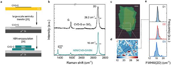
Figure 1. (a) Schematics of the samples' preparation: CVD-G single crystals are synthesized on Cu and transferred to SiO2/Si; afterwards, they are 'sandwiched' between hBN flakes by dry pick-up. (b) Representative Raman spectra of CVD-G on SiO2/Si (black) and of hBN/CVD-G/hBN (dark cyan; the two spectra are normalized at the 2D peak maximum). FWHM(2D) is indicated for the two curves. (c) Optical microscopy image of a typical hBN/CVD-G/hBN sample (scale bar is 10 μm). The gray dashed rectangle marks the region over which we perform scanning Raman mapping. (d) False-color map of FWHM(2D) over the area indicated in (c). FWHM(2D) < 18 cm−1 is measured over flat parts of the heterostructure (light blue), while interface bubbles give FWHM(2D) > 30 cm−1 (dark red). The black dashed rectangle indicates the part of the sample employed for fabrication of device D1. (e) Statistical distribution of FWHM(2D) measured on the active channels of devices D1–3. The color scale is the same as in (d).
Download figure:
Standard image High-resolution imageIn figure 2(a) we show the resistivity (ρ) of D1–3 as a function of the back-gate voltage (Vbg, applied to the underlying p-doped Si substrate) measured at room temperature and in vacuum (details on the measurement setup are given in Methods). The three devices show a narrow resistivity peak corresponding to charge neutrality, positioned at Vbg ⩽ 0.5 V, indicating minimal residual hole doping, with a maximum ρ0= 1.10–1.25 kΩ. Away from the neutrality region, ρ reduces to as low as 65 Ω (measured at Vbg = − 30 V in D1). Although Vbg can be applied to D3 only over a limited range (±2 V), due to an exponentially increasing leakage current, the narrow resistivity curve allows performing most of the relevant quantitative analysis also for this sample. In figure 2(b) we show a series of double-Log plots of the room T conductivity σ = 1/ρ as a function of the charge carrier density n= Cbg(Vbg−V0bg)/e (where e is the electronic charge, V0bg is the gate voltage at the charge neutrality point and the back-gate capacitance per unit area Cbg is determined by low-field Hall effect measurements, see figure S4). We observe a linear Log(σ) vs Log(n) dependence, followed by a saturation when n approaches ∼1010 cm−2. By intersecting a fit to the linear part with a horizontal line set at the minimum conductivity σ0= 1/ρ0, we estimate the charge carrier fluctuations n* for D1–3 to be within 3.2–4 × 1010 cm−2. This range corresponds to the expected concentration of thermally excited carriers at room T [31], implying that any disorder-induced inhomogeneity stands below this intrinsic broadening. For the sake of comparison, [21] reported n* in this order only at cryogenic temperatures. In figure 2(c) we show the mobility calculated according to the Drude model μD = σ/(ne) as a function of n for D1–3 (the regions |n| < n* are excluded, since they correspond to a regime of coexisting electrons and holes [32]). As typically observed in high-quality hBN-encapsulated graphene [11], the curves show a plateau in the vicinity of 1011 cm−2, where we observe a device-independent μD ∼ 1.2–1.3 × 105 cm2 V−1 s−1; for comparison, note that [21] reported values lower by approximately a factor two at equal n and T. With respect to CVD-G transferred on top of hBN [22], we observe a factor six increase in carrier mobility, highlighting the key role of dry hBN-encapsulation in probing the intrinsic electronic performance of the material. At higher carrier density, μD decreases due to electron-phonon scattering, as modelized by Hwang and Das Sarma [5], whose theoretical curve is plotted as a dashed line in figure 2(c) and represents a widely accepted upper bound for ideal environmentally-isolated single-layer graphene. In this sense, our data closely resemble the 'textbook' ones reported by Wang et al [11], which were obtained with exfoliated flakes. The recent findings on μD exceeding this limit in WSe2-covered CVD-G [33] obviously cannot be compared to our results due to the different dielectric material employed; nevertheless, the reference hBN-encapsulated CVD-G devices reported there [33] show inferior μD with respect to D1–2 over the whole n range considered. Additionally, in SI (figure S5) we show that σ(n) for D1–2 is well described by the relation σ−1= (neμL + σ0)−1 + ρs, where μL is a density-independent mobility (given by long-range scattering) and ρs is a constant resistivity offset (due to short-range scattering) [7]. We obtain (independently on the device) μL = 1.5 × 105 cm2 V−1 s−1 (1.2 ×105 cm2 V−1 s−1) for electrons (holes), roughly matching the μD plateau values, and ρs = 46 Ω (36 Ω) for electrons (holes), which corresponds to the expected magnitude of the resistivity due to electron-phonon coupling in ideal graphene [6].
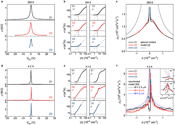
Figure 2. (a) ρ as a function of Vbg for devices D1–3, measured at room temperature (T = 300 K). (b) Double-Log σ(n) plots obtained from the data in (a), both for hole (left panels) and electron doping (right panels). The horizontal dashed lines are set at the minimum conductivity for each device, the oblique ones are linear fits to Log(σ)(Log(n)) and the vertical ones connect the intersection of the first two to the x axis, determining the estimate of n*. (c) μD as a function of n for devices D1–3. The dashed lines are calculations from the model of [5], showing the theoretical concentration-dependent phonon-limited mobility of graphene at room temperature. (d) Same as (a) but measured at liquid helium temperature (T = 4.2 K). (e) Same as (b) but from the gate-dependent data at T = 4.2 K shown in (d). (f) Same as (c) but at T = 4.2 K. The dashed lines are calculations for density-dependent ballistic transport over distances up to the widths of the Hall bars [34]. The inset shows separate enlarged views of the main panel for hole and electron doping, with Log scale on the x axis, highlighting the peak region of μD. The shaded rectangle indicates the averaging interval (0.75–1.25 × 1011 cm−2) used to calculate the values of μD reported in the text and in figure 3.
Download figure:
Standard image High-resolution imageFigure 2(d) shows ρ(Vbg) curves for D1–3 at T = 4.2 K. The resistivity peaks become extremely sharp and reach ρ0 =3.8–4.2 kΩ, while the smallest resistivity measured is 26 Ω (D1, Vbg = 25.8 V). The devices do not show diverging resistivity at the neutrality point, nor satellite peaks at large Vbg, thus confirming the rotational mismatch between CVD-G and the hBN flakes [12]. The cryogenic conditions suppress the thermally activated contributions and allow the observation of device-to-device variations in the width of the charge-neutrality peak, which reflect slight differences in the electrostatic disorder. To quantify this variability, we again employ double-Log σ(n) plots (figure 2(e)) and estimate n* = 6.6 × 10⁹–1.9 × 1010 cm−2 for the three devices. To the best of our knowledge, n* values in the 109 cm−2 range (obtained for D2–3), indicating extremely low potential fluctuations, have not been reported previously for CVD-G. Moreover, the device structure employed here is quite simple and does not include single-crystalline graphite gates that would further reduce n* by screening of remote disorder [13]. In figure 2(f) we plot μD for D1–3 as a function of n (solid lines, excluding the regions |n| < n*), together with μD = 4eW/(πh2 n)1/2 (dashed lines, where h is the Planck's constant), which is the expected carrier-dependent mobility for ballistic transport over distance W [34], which we set equal to the devices' width (2.5 μm, 2 μm and 3 μm for D1, D2 and D3, respectively). This functional dependence captures the general behavior of the samples at large n, indicating that the devices' finite dimensions represent the primary limitation to the carriers' motion. Deviations and noisy features are ascribed to contacts-related fluctuations in the four-probe signals, due to finite width of the contact arms (see figure S3) and high contact resistance (∼kΩ). In the low-density range, we observe a slight electron-hole asymmetry, with the highest mobility reached at |n| ∼ 1011 cm−2, where μD starts to approach the size-limited curves (see figure 2(f) inset). The peak values for D1–3 (averaged over a finite n interval to account for fluctuations in the resistance signals) are in the range 4.1–6.6 × 105 cm2 V−1 s−1 (2.1–3.6 × 105 cm2 V−1 s−1) for electrons (holes), and identify our devices as the highest performing CVD-G-based to date.
In figure 3 we analyze our findings by studying the correlation between mobility and charge fluctuations. We do so by considering both μD(∼1011 cm−2) (triangles) and the field effect mobility defined as μFE =(dσ/dn)/e (circles, where the slope dσ/dn is obtained over the linear regions visible in figures 2(b), (e)), both for electrons and holes (filled and empty symbols). μD and μFE—values of mobility estimated via two different methods in a similar carrier density range—show a reasonable agreement over the whole plot, corroborating the discussion above, which is based on the Drude mobility (μD). The data corresponding to measurements at 300 K collapse in a very narrow region, pointing at a universal behavior, i.e. determined solely by thermal broadening and insensitive to the sample details. When the devices are cooled to 4.2 K, the data show a more marked scattering, with D2–3 clearly positioning at higher μ and lower n* with respect to D1, reflecting the lower level of disorder. The overall behavior is well described by the relation μ−1 α n* by Couto et al [35] (dashed line in figure 3), as generally accepted for high-quality graphene on substrates.
To further support the observation of ultra-high carrier mobility in CVD-G, we measure the transport properties of D3 at T = 0.3 K, in the presence of a perpendicular magnetic field B. In figure 4(a) we show a false-color map of the longitudinal conductivity σxx = ρxx/(ρxx2 + ρxy2) as a function of Vbg and B (up to 200 mT), where a typical fan of Landau levels (LL) can be appreciated. The condition to observe this phenomenology is governed by the competition between the cyclotron gap separating the LL  (where N is the LL index) and the disorder-induced level broadening Γ = ħ/2τq, where τq is the so-called quantum scattering time, which quantifies the carriers' scattering in presence of B. When a large enough field Bonset is applied, Δc equals Γ and the conductivity begins to oscillate, thus composing the fan-shaped diagram. In D3 we observe Bonset as low as ∼50 mT for the first oscillations at filling factor ν = nh/eB = ± 2, while it increases to ∼100 mT for larger fillings (see light-red-to-white colored areas). In figure 4(b) we show τq as a function of n, extracted from the onset field of the oscillations (see SI, figure S6 for details on determination of Bonset). Close to charge neutrality, we observe τq< 0.1 ps due to residual disorder in the n*-region, with a marked growth to ∼0.15 ps at higher density. To the best of our knowledge, the largest τq reported for graphene is 0.3 ps by Zeng et al [36], who made use of exfoliated graphene, hBN-encapsulation and top and bottom graphite gates. The × 2 factor over our values (which, interestingly, corresponds to the difference in n* between D3 and their sample) can be mostly ascribed to the screening effect of the single-crystalline gates. Restricting our comparison to CVD-G only, [18] reported Bonset = 400 mT at T = 1.6 K, while [21] showed resolved LL at 1.8 T and 9 K. In figure 4(c) we show that the low-field oscillations lead to a fully developed quantum Hall effect already at B = 200 mT, with zeroes in σxx accompanied by quantized Hall conductivity σxy = ρxy/(ρxx2 + ρxy2) following the half-integer sequence of single-layer graphene [3, 4]. These observations prove ultra-low LL broadening and suggest the possibility of accessing correlation-driven phenomena making use of CVD-G. In figure 4(d) we show additional magnetotransport data on D3 (up to 12 T), where, starting from ∼1 T, interaction-induced broken-symmetry states [37] are observed at ν = − 3, −1 and 0. At charge neutrality (ν= 0) the sample becomes fully insulating for B > 3 T (figure 4(e)), as expected for an interaction-induced spin-valley antiferromagnet [38]. Along filling factor ν= − 1/3 (gray dashed line in figure 4(d)), we observe a zero-resistance region for B ⩾ 8.5 T, indicating a fractional quantum Hall (FQH) state [39, 40]. In addition to vanishing longitudinal resistance, quantum Hall states result in plateaus at |ν|× e2/h in the two-terminal conductance G = ISD/VSD and ν× e2/h in σxy. Our measurements show plateau-like features, where G∼ 1/3 × e2/h (figure 4(f)), while σxy stands far from the expected value (figure 4(f), inset). In the SI we consider possible origins for this discrepancy and discuss how, in addition to higher magnetic field sources, more specialized device structures are likely needed for a thorough investigation of FQH in CVD-G. Nevertheless, FQH states require ultra-clean two-dimensional electronic systems [41], among which hBN-encapsulated CVD-G is to be included.
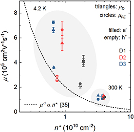
Figure 3. Mobility as a function of n*, summarizing our results for D1–3, both at room and liquid helium temperature. The triangles are estimates from the Drude model at carrier concentration ∼ 1011 cm−2 (the error bars are standard deviations over the averaging interval). The circles are field-effect mobility (the error bars are from the linear fits to σ(n)). The filled (empty) symbols are for negatively (positively) charged carriers. The dashed line is a model from [35], describing an inverse proportionality between μ and n*.
Download figure:
Standard image High-resolution image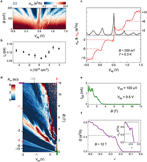
Figure 4. (a) False-color map of the longitudinal conductivity of D3 as a function of back-gate voltage and magnetic field. The logarithmic color scale is chosen to highlight the Landau level fan and the low-field onset of the oscillations. (b) Quantum scattering time as a function of the carrier density, obtained from the onset field as described in the text. (c) Longitudinal (black) and Hall conductivity (red) of D3 as a function of the back-gate voltage at fixed field B = 200 mT. The horizontal dashed red lines indicate the plateau values of the half-integer quantum Hall effect in graphene monolayer. (d) False-color map of the longitudinal resistance of device D3 as a function of back-gate voltage and magnetic field. The four-fold degenerate integer quantum Hall states (−2, − 6, − 10) are labeled in black, the broken-symmetry integer quantum Hall states (0, − 1, − 3) in red, the − 1/3 fractional state in gray. The gray dashed line indicates filling factor ν= − 1/3. (e) Source-drain current as a function of the magnetic field, measured at charge neutrality (green mark in (d)). (f) Two-terminal conductance as a function of the filling factor, measured at the highest magnetic field at disposal, B = 12 T (purple mark in (d)). The curve is corrected by considering a contribution from contact resistance of 6.2 kΩ, estimated from the offset in the conductance plateau value at ν = − 2, B = 2 T (increased contact resistance at 12 T likely accounts for the imperfect quantization). The inset shows the Hall conductivity under the same conditions. All the data are acquired at T = 0.3 K.
Download figure:
Standard image High-resolution image
3. Conclusion
In conclusion, we presented unprecedented electrical transport performances for CVD-G. We synthesize and transfer single-layer graphene crystals using scalable approaches, and subsequently make use of hBN-encapsulation to investigate their intrinsic electronic response. Our devices mimic the transport properties of equivalent samples (micrometer-sized and Si-gated) based on micro-mechanically exfoliated flakes, including room-T mobility exceeding 105 cm2 V−1 s−1, onset of Landau quantization at ultra-low field, and signatures of FQH. While preparing this manuscript, we became aware that CVD-G detached from Cu via hBN-mediated dry pick-up, under high magnetic fields, shows similar evidence of FQH [42]. In addition to the high electronic quality of CVD-G, our work highlights a major weakness in the status of technological application of graphene, i.e. the lack of a large-scale analogue of hBN single-crystals. Although large-area few-layer hBN can be synthetized by CVD on metals, such material does not provide adequate environmental screening, resulting in poor graphene mobility if compared to devices employing exfoliated hBN flakes [43]. Regarding the use of CVD-G in fundamental research topics, this would require several improvements over the samples presented in this work. Apart from modifications in the device structure, increasing the size of the processable (bubble-free) regions within the hBN/CVD-G/hBN heterostructures is a clear priority. Engineering clean interfaces over large areas in CVD-G-based hetero-stacks is also of great technological relevance and might benefit from assembly in vacuum conditions [44], and post-assembly thermal and/or nano-mechanical treatment [31]. Moreover, large-area high-quality CVD-G carries considerable potential for the rising field of twisted bilayer graphene (TBG) [45], where the use of techniques such as micro-arpes and optical spectroscopies is currently limited due to the size of samples obtained via tear-and-stack of an individual exfoliated flake [46]. Since CVD-G single-crystals grown within the same mm-sized Cu grain are crystallographically aligned to each other [22], different crystals can be stacked with the required angular accuracy, facilitating large-scale studies of TBG. As an alternative, large-area TBG can be obtained via synthesis of CVD-bilayers with growth-controlled twist angle [25]. However, stabilizing small and accurate rotational shifts from the energetically favored Bernal stacking, as required for 'magic-angle' TBG [45], poses significant challenges.
4. Methods
Chemical vapor deposition: We synthesize the graphene single crystals on electropolished Cu foils by CVD in a commercial reactor (Aixtron 4" BM-Pro), set at p = 25 mbar and T = 1060 °C. The Cu foil is annealed in Ar flow for 10 min at T = 1060 °C. The growth takes place for 15 min in 90% Ar, 10% H2 and 0.1% CH4. A quartz enclosure controls the gas flow on the sample [23], limiting the nucleation density.
Raman spectroscopy: We use scanning Raman spectroscopy to characterize the samples based on CVD-G. We employ a Renishaw InVia confocal spectrometer equipped with a 100 × objective, with laser light at 532 nm wavelength, at ∼1 mW laser power. The Si peak at 520 cm−1 is used to calibrate the spectra.
Device fabrication: We process the hBN/CVD-G/hBN samples by e-beam lithography, reactive ion etching and thermal evaporation of metals. We first pattern the Hall bar mesa and etch the samples in CF4/O2. A second PMMA mask, followed by metal evaporation and liftoff, is used to define the electrical contacts (Cr/Au 5/70 nm), which connect to CVD-G via the exposed edges of the heterostructure [11]. The devices are glued on dual-in-line chip carriers using Ag conductive paste and wire-bonded with Al wires.
Electrical transport measurements: measurements at room T are carried out in a vacuum chamber (base pressure p ∼ 10–5 mbar), with electrical connections to a dual-in-line holder. The low T data are acquired in a 4He cryostat with superconducting coil for Hall effect measurements. In both cases, we use AC lock-in detection (13–17 Hz) in constant current configuration (10–100 nA). D3 is further tested in a 3He refrigerator providing additional cooling down to 0.3 K. The data in figures 4(d)–(f) are acquired in a constant voltage configuration (VSD = 100 μV), measuring, in addition to the longitudinal and Hall voltage drops, the source-drain current.
Acknowledgments
Growth of hexagonal boron nitride crystals was supported by the Elemental Strategy Initiative conducted by the MEXT, Japan, Grant Numbers JPMXP0112101001, JSPS KAKENHI Grant Numbers JP20H00354 and the CREST(JPMJCR15F3), JST. This project has received funding from the European Union's Horizon 2020 research and innovation programme Graphene Flagship under grant agreement No 785219 and No 881603.