
Abstract
Phononic crystals (PnCs) are artificially patterned media exhibiting bands of allowed and forbidden zones for phonons—in analogy to the electronic band structure of crystalline solids arising from the periodic arrangement of atoms. Many emerging applications of PnCs from solid-state simulators to quantum memories could benefit from the on-demand tunability of the phononic band structure. Here, we demonstrate the fabrication of suspended graphene PnCs in which the phononic band structure is controlled by mechanical tension applied electrostatically. We show signatures of a mechanically tunable phononic band gap. The experimental data supported by simulation suggests a phononic band gap at 28–33 MHz in equilibrium, which upshifts by 9 MHz under a mechanical tension of 3.1 N m−1. This is an essential step towards tunable phononics paving the way for more experiments on phononic systems based on 2D materials.
Export citation and abstract BibTeX RIS

Original content from this work may be used under the terms of the Creative Commons Attribution 4.0 license. Any further distribution of this work must maintain attribution to the author(s) and the title of the work, journal citation and DOI.
1. Introduction
The periodic arrangement of atoms in solids gives rise to the band structure for electrons and with it to all the richness of solid-state physics. During the last decades, artificial periodic patterning of materials on a much larger length scale, spanning tens of nanometers to meters, has been used to induce a band structure for phonons in so-called phononic crystals (PnCs) [1–4]. PnCs have been used as widely re-configurable analogues of solids to study phenomena ranging from a metal-insulator transition [5] to topological states [6, 7], and acoustic flatbands [8, 9]. In addition, phononic band gaps have been employed to decouple localized vibrational modes from their environment resulting in ultra-coherent resonances suitable for storing quantum information [10–12].
There is one feature of traditional solid-state crystals that is so far elusive in PnCs: in-situ tunability. The band structure parameters of solids can be adjusted via e.g., electrostatic gating, application of magnetic fields, or mechanical straining. Such tunability allows a plethora of experiments ranging from the exploration of phase transitions to changing the band structure topology [13–18], or increasing the electron mobility in silicon [19–21]. In contrast, phonons in PnCs do not react to an electrical or magnetic field. In addition, many of the materials used to create PnCs, such as silicon or silicon nitride, are rigid and cannot be mechanically manipulated in-situ.
Graphene, as well as other two-dimensional materials, hold promise for tunable PnCs [5, 22–25]. From one perspective, graphene can be directly patterned down to a near-atomic length scale while supporting a variety of phononic lattices. In addition, graphene is a strong yet flexible material capable of withstanding tension as high as 42 N m−1 (∼10% of strain) without breaking [26]. These properties, in combination, suggest that mechanically tunable graphene PnCs can be created [22]. Nevertheless, the challenges associated with creating large-area, uniform graphene membranes in combination with a challenging detection of high-order modes prevented experimental demonstration of tunable graphene PnCs so far.
Here, we demonstrate the design and characterization of a functional tunable graphene PnC. The device is made from a suspended large-scale (10 μm radius) few-layer graphene membrane, which is artificially patterned with a uniform honeycomb lattice of holes. This step transforms it into a PnC and gives rise to a phononic band structure, which ultimately determines any mechanical motion within the device. We use interferometric measurements to establish the band gap for out-of-plane acoustic phonons in the MHz range within the structure. We then show that additional tension up to >3 N m−1 can be induced using electrostatic gating. In response to that increase in tension, we observe signatures consistent with an upshift of the phononic band gap of 9 MHz (∼29%).
2. Results
2.1. Sample design and fabrication
Our design of a mechanically tunable PnC requires a suspended graphene membrane so that the tension can be controlled by applying a voltage. This puts the natural limitation on device size as it is hard to create free-standing graphene with radii larger than 10 μm [27]. In order to improve the uniformity and to make the sample less sensitive to surface contaminations, we use a trilayer graphene. This comes at the cost of a reduced tunability compared to a monolayer sample but is necessary to clearly define a phononic band gap. To create the PnC structure, we pattern a regular honeycomb lattice of holes (diameter d) in the suspended graphene membrane. The unit cell and the corresponding first Brillouin zone of this lattice are shown in figure 1(a). The position and size of the phononic band gap in the structure depend on lattice parameter a, the ratio d/a, and the initial tension  in the membrane. We chose d/a= 0.522 which maximizes the band gap size. For choosing the lattice parameter, we need to find a compromise. Ideally, we want to make a as small as possible, to fit a large number of unit cells into the finite suspended area. However, small lattice constants result in a high frequency range for the band gap, which will make the detection challenging, in terms of suitable detectors and electronics. Therefore, we use a lattice parameter of a = 1.36 μm, which corresponds to a PnC with approximately 7 unit-cells across in the armchair direction and 13 in the zigzag direction. Our fabrication protocol allows us to reproducibly pattern PnCs down to a lattice parameter a ∼100 nm. For smaller parameter values, the bridge separating the holes becomes narrower than 10 nm, and samples tend to break at this point. The final parameter of our PnC—the built-in tension in the sample—is beyond our control. An annealing step before pattering helps to reduce the tension as far as possible and cleans the device from fabrication-related residues. We calculate the phononic band structure of the PnC with these parameters and a built-in tension of 0.44 N m−1 (obtained from experiments shown below) by matching the vibrational frequencies to a simulation in COMSOL (figure 1(b)). For this phononic lattice, we find a band gap between 28 and 34 MHz for out-of-plane modes. We note that only out-of-plane acoustic phonon modes are considered here, as they are most relevant in PnCs made from 2D materials because they are easy to excite and detect.

Figure 1. Device design and measurements. (a) PnC unit cell and first Brillouin zone used for band structure calculations. (b) Phononic band structure for out-of-plane modes of the PnC obtained using an 'infinite' model, along with the corresponding density of states (DOS). (c) Scanning electron micrograph of the fabricated phononic crystal device using the lattice parameters from (a). (d) Experimental setup used for interferometrically measuring vibrational spectra. QWP is a quarter wave plate, PBS stands for polarizing beam splitter, BT labels a bias-tee, and PD is the photodetector. (e) Vibrational spectrum of the device shown in (c) at zero applied gate voltage (built-in tension = 0.44 N m−1). The grey trace shows the noise floor of the setup (sample actuation off). The region of the phononic band gap is shown in blue. In the band gap region, we find a strongly suppressed response, which falls in the noise floor of the experiment. (f) Simulated vibration spectrum of the same device.
Download figure:
Standard image High-resolution imageTo fabricate this structure, we use electron beam lithography and metallization on a SiO2/Si wafer to define a hard mask for a subsequent wet-etching step (details in SI). After the etching, we have a ∼1 μm deep pit in the substrates on which we transfer an exfoliated trilayer graphene flake using the polymer (Polydimethylsiloxane, PDMS) stamp dry transfer [28–31]. This leaves us with a suspended graphene membrane, which is electrically contacted via the gold layer. We chose thin multilayer exfoliated graphene to reduce wrinkling in the device, for band gap uniformity and sample stability. Finally, the phononic lattice discussed above shown in figure 1(a) is cut in the graphene using a focus ion beam (figure 1(c)) [32]. In designing the device, our goal was to obtain high-uniformity devices with predictable boundary conditions yielding a well-defined band gap.
2.2. PnC measurements
The PnC is measured inside a homebuilt vacuum chamber with base pressure better than 1.3 × 10⁻⁵ mbar (figure 1(d)). To drive the device, we use electrical actuation (an AC + DC voltage applied between the graphene and Si backgate, figure 1(d)) for its high efficiency and because it induces less heating and photodoping than e.g., optothermal actuation. By adjusting the DC component (Vg) of the applied voltage, we can tune the applied electrostatic pressure on the PnC and thus the tension in the suspended area. For detection, we use a 632.8 nm HeNe laser that is focused on the PnC. The suspended membrane and the backgate form a Fabry-Pérot interferometer along the z-direction and the reflected signal is thus modulated by the out-of-plane oscillation of the membrane [33]. We detect this signal in an avalanche photodetector (PD in figure 1(c)). To increase signal-to-noise ratio, we insert a 5 mm aperture before the PD.
The measurements of PnCs require resolving high-order vibrational modes which in general have very low vibrational amplitude. Therefore, multiple approaches to optimize the sensitivity of our detection scheme are needed. We adjust the cavity length in the etching step to maximize the interferometric signal (see SI), we also use a polarized laser beam in combination with a polarization beam splitter and a quarter wave plate that allows us to guide almost 100% of the reflected light into the PD. Finally, we implement a pinhole, which cuts out unwanted reflected light, and thereby reduces the laser noise in our detection scheme (details in SI). Overall, we obtain a displacement sensitivity better than 0.5 pm/ (see SI).
The measured vibrational spectrum of our PnC is shown in figure 1(e). We observe the fundamental mode at 2.97 MHz and ∼35 subsequent modes above the noise level. We track the fundamental modes vs. applied gate voltage and extract the built-in tension T0 as well as the mass density  of the device from fitting the capacitive softening regime (see SI). We find
  and
and  , respectively. These parameters are used as inputs for the simulations in figures 1(b) and (f). We prefer to use tension rather than strain as our key parameter since the former ultimately determines the frequency of our resonator (
 ) while the latter depends on the Young's modulus of the patterned device, which is hard to measure directly. The extracted value for mass density is about 23 times higher compared to what is expected for pristine graphene, likely due to the impurities always present on the surface of 2D materials.
While we find a densely populated 'forest' of vibrational modes at frequencies above the fundamental mode, we see a region of strong suppression between 28 and 33 MHz (blue in figure 1(e)). This region is exactly where the band gap is expected from our band structure calculation. To better understand this spectrum, we carry out a 'finite' simulation accounting for the finite size of the PnC and considering the boundary conditions of the device. We can directly compare our experimental vibrational spectra (figure 1(e)) to the outcome of the simulation (figure 1(f)). We see a matching phononic band gap in both graphs, as well as similar peaks on both sides of the band gap, comparable to the peaks in the phononic density of states associated with flat bands at both sides of the band gap (figure 1(b)).
We note that the simulation does not match the measurements perfectly. This is likely due to unavoidable stress non-uniformity in our devices caused by nonlinearity of the cut drum-head and variations in boundary conditions. While the frequencies of modes from circular-membrane systems are strongly affected by these effects, the position of the phononic band gap is relatively insensitive to them. It is also noteworthy that both the simulation and experiments show modes inside the band gap. These are localized states related to the finite size non-patterned edges of our system (details in SI). Finally, it should be noted that the measurements are limited by the size of the laser spot size preventing us from resolving most of the modes with frequency much higher than the band gap. When we compare our data to measurements of non-patterned devices (see SI), we find only a few (∼5–8) lowest frequency modes compared to N > 35 in the patterned PnC sample. Also, we do not find a region of suppressed displacement in the reference samples (see SI). Both points highlight the effects of the phononic order in our devices.
2.3. Tuning PnCs
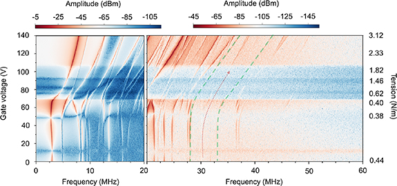
Our next goal is to explore changes in vibrational spectra with induced tension and show in-situ tunability of our phononic system. As we vary the DC component of the gate voltage, we observe a smooth evolution of the vibrational spectrum with the fundamental mode downshifting from 2.96 MHz to 2.74 MHz and then upshifting to 7.92 MHz (figure 2). The initial downshift is due to the so-called capacitive softening [34–38], while the upshift is caused by the increase of tension. The higher order modes show a variety in different tuning behavior, which we attribute to a combination of photothermal backaction effects [39–41] and different coupling to the electrostatic field for different modes [42–44]. While there are interesting interactions taking place, this is not the scope of the work. We assume that the application of DC voltage produces tension,  , where f0 and f are the values of the fundamental mode frequency before and after the application of gate voltage. We find that we generate up to T − T0
=2.68 N m−1 additional tension at our highest Vg = 140 V.
, where f0 and f are the values of the fundamental mode frequency before and after the application of gate voltage. We find that we generate up to T − T0
=2.68 N m−1 additional tension at our highest Vg = 140 V.
Figure 2. Tension-dependence of the PnC. Vibrational spectrum of a phononic crystal device vs. applied gate voltage, which is controlling the tension. The regions around the fundamental mode as well as the entire spectrum are shown separately. Dashed green lines denote edges of the phononic band gap, which tunes by ∼29% for the highest applied voltage.
Download figure:
Standard image High-resolution image
We now analyze the evolution of the phononic band gap region, which spans from 28 to 33 MHz at zero Vg. Experimentally, we find that the region upshifts together with other modes for increasing Vg. Using an effective spring constant extracted from the fundamental modes, we can simulate the evolution of the phononic band gap (green line in figure 2). We find that that region upshifts by 9 MHz at our highest tension. The region preserves a low vibrational amplitude. At the same time, we observe the appearance of new vibrational peaks inside it. This behavior also seen in simulations likely corresponds to new defect modes activated by the gradual violation of the translational symmetry and stronger drive power at higher voltages. Overall, the data in figure 2 suggest that the phononic band gap in the graphene PnC is mechanically tunable by 9 MHz (29%). Comparing this to previous theoretical predictions [22], we find an order of magnitude lower tunability upon applying a comparable pressure. This is due to the larger stiffness and increased built-in tension in the trilayer devices compared to monolayer samples (T0 = 0.01 N m−1) used in [22]. Furthermore, we can compare our results to another tunable phononic system made from graphene [23]. In this approach, the graphene membrane is clamped by many pillars forming a regular array. While the system is more rigid, it can be tuned by approximately 10%–15%. The device does not feature a phononic band gap.
3. Discussion
In conclusion, we developed an approach to fabricate suspended gate-tunable graphene PnCs and observed signatures of phononic band gap variation in these devices. These results suggest several interesting pathways for further work. First, it is instructive to consider the factors limiting the quality of our graphene PnCs. One of them is the device size limiting the number of unit cells inside the PnC (currently 57). Better growth and transfer techniques may help to increase this number. Another limitation is non-uniformity inside the device coming primarily from uneven edges of the hole pattern, unavoidable wrinkling in graphene, and the gold contacts. We anticipate that it may be possible to produce more uniform devices by employing 'additive' manufacturing strategies where additional material is deposited onto graphene to create periodic PnCs. This will pave the way for interesting applications of tunable phononic systems. These include, for instance, tension-tunable in-gap mechanically shielded defect modes as well as exploring mechanical analogues to phase transition in condensed matter systems. Second, the quality of our measured spectra is limited by the diffraction-limited size of our read-out probe making it challenging to access higher-lying vibration modes. Near-field techniques such as scanning near-field optical microscopy may be employed to break this barrier [45, 46]. Third, our approach for tuning artificial lattices is not limited to PnCs and, in principle, allows us to also induce tunable features in photonic [47, 48], plasmonic-phononic [49, 50], or Moiré lattices [51] made from 2D materials. Finally, it will be interesting to explore the role of the inherent displacement non-linearity of graphene on phononic spectra. Our devices are especially suitable for this task since the patterning effectively softens the membrane resulting in large oscillation amplitudes and therefore strong non-linear effects.
Acknowledgments
This work was supported by Deutsche Forschungsgemeinschaft (DFG, German Research Foundation, project-ID 449506295 and TRR 227 B08, 328545488), EU COST Action CA 19140 (FIT4NANO) and CSC 202006150013. The Ga ion beam patterning was performed in the Corelab Correlative Microscopy and Spectroscopy at Helmholtz-Zentrum Berlin.
Data availability statement
The data cannot be made publicly available upon publication because no suitable repository exists for hosting data in this field of study. The data that support the findings of this study are available upon reasonable request from the authors.
Supplementary data (1.1 MB PDF)