
Abstract
Large, 3D curved electronics are a trend of the microelectronic industry due to their unique ability to conformally coexist with complex surfaces while retaining the electronic functions of 2D planar integrated circuit technologies. However, these curved electronics present great challenges to the fabrication processes. Here, we propose a reconfigurable, mask-free, conformal fabrication strategy with a robot-like system, called robotized 'transfer-and-jet' printing, to assemble diverse electronic devices on complex surfaces. This novel method is a ground-breaking advance with the unique capability to integrate rigid chips, flexible electronics, and conformal circuits on complex surfaces. Critically, each process, including transfer printing, inkjet printing, and plasma treating, are mask-free, digitalized, and programmable. The robotization techniques, including measurement, surface reconstruction and localization, and path programming, break through the fundamental constraints of 2D planar microfabrication in the context of geometric shape and size. The transfer printing begins with the laser lift-off of rigid chips or flexible electronics from donor substrates, which are then transferred onto a curved surface via a dexterous robotic palm. Then the robotic electrohydrodynamic printing directly writes submicrometer structures on the curved surface. Their permutation and combination allow versatile conformal microfabrication. Finally, robotized hybrid printing is utilized to successfully fabricate a conformal heater and antenna on a spherical surface and a flexible smart sensing skin on a winged model, where the curved circuit, flexible capacitive and piezoelectric sensor arrays, and rigid digital–analog conversion chips are assembled. Robotized hybrid printing is an innovative printing technology, enabling additive, noncontact and digital microfabrication for 3D curved electronics.
Export citation and abstract BibTeX RIS

Original content from this work may be used under the terms of the Creative Commons Attribution 3.0 license. Any further distribution of this work must maintain attribution to the author(s) and the title of the work, journal citation and DOI.
1. Introduction
The demand for large-area, 3D curved electronics that offer the electrical functions of conventional, 2D planar integrated circuit (IC) technologies and simultaneously conform on complex surfaces has been increasing for emerging applications, such as tactile sensation in robots [1], smart skins for aircrafts [2], structural health monitoring [3], and hemispherical electronic eye cameras [4]. Current electronics are fabricated on 2D planar, rigid, and brittle substrates, such as silicon wafers and glass plates, however, they are intrinsically incompatible with large-area, 3D curved surfaces [5]. Furthermore, the kinds of curved electronics that integrate flexible sensors, rigid chips, and large-scale interconnected circuits have revolutionized microfabrication, from 'small-area' to 'large-area', from 'planar' to 'curved', and from 'rigid' to 'flexible' [6, 7]. However, the inherently 2D planar nature of the patterning, deposition [8], and etching to photolithography [9] faces significant challenges.
Several technologies have been proposed in the primary stage of curved electronics, which can be roughly classified into three classes: controlled deformation of stretchable electronics [10, 11], microcontact printing with soft stamps [12], and inkjet printing via robots [13–15]. Stretchable electronics that are fabricated by 2D microfabrication and transfer printing can assemble planar electronics onto a rigid, deformable or time-dynamic curved surface directly in a passive or active conformational manner [12, 16–19]. These approaches have turned out to be a common strategy for manufacturing high-performance curved electronics that are comparable to traditional microelectronics. Nevertheless, efforts should still be devoted to conformally mounting flexible/stretchable electronics on high-curvature surfaces. Simultaneously, the size of the curved electronics is limited by that of the wafers used in fabrication.
On the other hand, inkjet printing directly deposits functional materials on complex surfaces and represents another promising technique for curved electronics [20–22], though they are frequently adopted in 2D planar patterning. When inkjet printing incorporates robotic systems, it is more flexible in the fabrication of complex curved electronics, including the geometric topology, feature size, functions/materials, and the order of processes, which provides a promising solution for the fabrication of curved electronics. Fortunately, robotic inkjet printing can be significantly extended to fabricate components, such as interconnected [23], embedded sensors [24] and structural electronics [25]. However, the patterning resolution and droplet sliding on complex surfaces are two long-standing issues for inkjet printing, where the resolution is typically larger than 20 μm and ultralow viscosity droplets inevitably slide on curved surfaces.
Herein, we propose a robotized 'Transfer-and-Jet' printing, which combines transfer printing and electrohydrodynamic (EHD) printing in a programmable and modular manner. It can relieve the limitations of the 2D planar microfabrication process and the low-resolution of conventional inkjet printing, to form large-area and high-performance curved electronics directly on an arbitrary surface. It adopts a robot-like system to integrate the measuring, planning, and execution systems to monitor the printer, circuit and tool states, and autonomously control relevant parameters via the measurement data and the process knowledge. The transfer printing is adopted to peel small rigid chips or ultrathin (∼1 μm) flexible electronics from 2D planar substrates via pick-and-place or laser lift-off (LLO) methods and so a dexterous robotic palm (a home-made end-effector) can transfer them onto 3D curved surfaces. The EHD printing is developed to conformally deposit diverse-viscosity functional ink (e.g. 1–10 000 cps) to generate fine patterns (e.g. featured size <1 μm) on large-area, curved surfaces. Several kinds of curved electronics are prepared to show the feasibility of robotized hybrid printing, including a smart skin for an aircraft, conformal antenna, and curved heater. Compared with the existing alternative approaches, this method provides a powerful new method assemble curved electronics, especially for the research-and-development type production that integrates design, testing, and manufacturing to markedly reduce the production cycle.
2. Features and fabrication requirements of large-area, 3D curved electronics
Figure 1(a) schematically shows a typical curved electronic system, such as a large-area smart sensing aircraft skin, which is integrated with a group of electronic and functional units on a curved surface, including microprocessor chips, conformal antennas, flexible sensors, interconnections/circuits, and functional microstructures. There are several featured characters that differ from traditional microelectronics. Firstly, the geometric shape of the substrates becomes complex, such as nondevelopable or freeform surfaces, and the curvature radius reaches <1 mm. Secondly, the integrated-electronic-area is usually much larger than a wafer (>1 m2). Thirdly, mass chips with different geometry are integrated on a curved surface, where the size ranges from 100 μm to 1 cm, and the thickness is from 50 μm to 1 mm. Furthermore, flexible sensors (thickness <20 μm) with or without stretchability have to be transferred from a planar substrate to a curved substrate. Additionally, the pins of rigid chips and flexible electronics are positioned either upward or downward. Fourthly, a high-resolution photoresist patterning needs to be formed directly on a curved surface for photolithography. Finally, massive interconnect wires should be fabricated on a curved surface to link all these chips and sensors together. The assembly technique of such electronics is far beyond the well-developed 2D planar technologies. Therefore, it adapts to electronic devices of various sizes and thicknesses and with or without stretchability. This assembly technique can transfer devices from a 2D planar substrate to a 3D curved substrate. The patterning technique has the capability of high resolution, and works well on curved surfaces in an additive, subtractive, or equivalent manner. Therefore, a general fabrication method for curved electronics is still in high demand from the aspect of processes and applications.
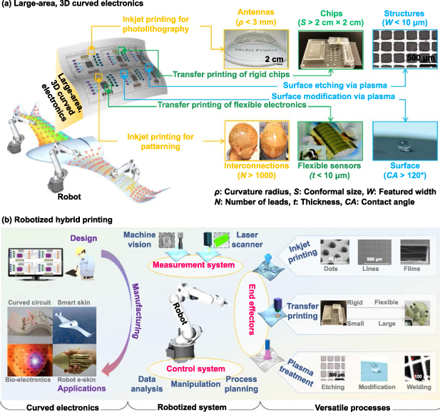
Figure 1. (a) Schematic diagram of a large-area smart skin for an aircraft integrated with large-area, 3D curved electronics, including conformal antennas, conformal interconnections, rigid chips, flexible electronics, microstructures, and a functional surface. Reproduced with permission from [21, 26–30]. Copyright 2018, John Wiley and Sons. Copyright 2021, American Chemical Society. Copyright 2014, AIP Publishing. Copyright 2019, Springer Nature. Copyright 2018, Royal Society of Chemistry. Copyright 2020, Elsevier. (b) The robotized 'Transfer-and-Jet' printing as a manufacturing strategy bridges the computer design and practical applications of large-area, 3D curved electronics on complex surfaces, where versatile processes (e.g. inkjet printing, transfer printing, plasma treating) can be permuted and combined for various goals. Reproduced with permission from [21, 26, 27, 30–39]. Copyright 2017, John Wiley and Sons. Copyright 2016, Cambridge University Press. Copyright 2014, Springer Nature. Copyright 2012, Springer Nature. Copyright 2019, IOP Publishing. Copyright 2019, SPIE. Copyright 2020, Elsevier. Copyright 2018, John Wiley and Sons. Copyright 2021, American Chemical Society. Copyright 2019, Springer Nature. Copyright 2014, AIP Publishing. Copyright 2020, Elsevier. Copyright 2017, IOP Publishing.
Download figure:
Standard image High-resolution imageFigure 1(b) schematically illustrates robotized 'transfer-and-jet' printing as a novel manufacturing strategy to bridge the computer design and practical applications of large-area, 3D curved electronics on complex surfaces. The robotized system consists of a robot-like system that integrates LLO, transfer printing, EHD printing, and plasma processing, etc. The involved processes can be digitalized and combined by programmable robotization techniques including the measuring system (e.g. laser scanner, machine vision, laser-energy meter), data analysis system (e.g. surface reconstruction and localization), process planning system (e.g. path planning, process optimization), and manipulation system (e.g. motion stage, dexterous robotic palm). Firstly, the computer model of curved electronics matches the practical substrate through a laser scanner and machine vision. Then it utilizes the control system to realize data analysis, manipulation, and process planning. Finally, the robotized hybrid printing fabricates the electronic system via the permutation and combination of inkjet printing, transfer printing, and plasma treatment in a point-by-point, noncontact, and programmable manner. The end effectors should be changeable and flexible for high compatibility with various processes. Additionally, the processes should be able to adopt themselves to complicated and changeable requirements to realize different types of fabrication with the limited tools. For example, inkjet printing should be able to directly fabricate dots, lines, and films with various materials. Transfer printing should be able to strip, pick, and transfer both the small, rigid chips and the large, flexible electronics. The plasma process should be able to etch, modify, and weld various films.
A typical 3D curved electronic system is adopted to exhibit the manufacturing process in detail. Firstly, 3D laser positioning is introduced to identify the point cloud of an arbitrary curved surface and then reconstruct it to obtain its geometric shape. This is helpful for matching the model between the computer and the objective substrate and assists the process planning. Secondly, the electronics that are fabricated through 2D microfabrication technologies become flexible via LLO. A dexterous robotic palm transfers the electronics from the 2D donor substrate to the 3D curved surface. The tool can precisely deform into a specific geometric shape of specific curved surface. Thirdly, digital plasma processing is usually adopted along the trajectory to enhance the adhesion between the substrate and the functional ink or photoresist. Furthermore, the plasma jet can etch the substrate without a physical mask. Fourthly, the interconnection circuits are fabricated through inkjet printing of photoresist for etching or of conductive inks, before or after the transfer printing of devices, respectively. The permutation and combination of these processes can realize versatile fabrication. If the size of the curved electronics is larger than the workspace of the robotized equipment, the curved substrate can be repositioned against the machine for subsequent cycles until the entire electronics system is completed.
3. Key techniques of robotized hybrid printing
Robotized equipment can change its topological structure and select the required processes and measurement system in a combine-on-demand manner [40]. Therefore, there are several key techniques that are unique to curved electronics. (a) Surface mapping for coordination matching, localization, and conformal design, based on which one can register the practical surface with the design surface, position the fabrication point through machine vision, and design the curved electronic system in planar space. (b) The technique should exhibit high compliance with the topological geometry of the surface and the size and rigidity of the electronic devices, based on which rigid chips and flexible electronics can be integrated in a programmable manner. (c) The process should be versatile, high-resolution, and highly compatible with various solutions, so more structures can be directly fabricated using fewer end effectors. (d) The technique should be a noncontact, light load, continuous process that is insensitive to error in normal directions to prevent the weakness in the robot, such as low precision and low rigidity.
3.1. Robotic surface mapping for coordination match, design and localization
In conformal fabrication, surface mapping is a key technology in coordination matching between the model (design space) and the object (workspace), precise positioning for surface registration, and assembly of curved surface from planar pattern. It differs from planar techniques, where the patterns keep the same in the design space and workspace. There are three kinds of mapping strategies, as shown in figure 2.
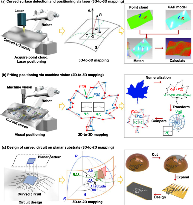
Figure 2. Surface mapping technologies in robotized hybrid manufacturing. (a) 3D-to-3D mapping for coordination via laser displacement sensor. Reproduced with permission from [36]. Copyright 2019, SPIE. (b) 2D-to-3D mapping for precise positioning via machine vision. Reproduced with permission from [35]. Copyright 2019, IOP Publishing. (c) 3D-to-2D mapping for assembly of curved surface.
Download figure:
Standard image High-resolution image3.1.1. '3D-to-3D' mapping for coordination matching via a laser displacement sensor.
The 3D design model must match with the 3D machining model for global positioning before fabrication. This step is not used in 2D planar microfabrication. A 3D measuring system based on a laser displacement sensor that is fastened to a high-precision motion platform was used to gain the point cloud to reconstruct the geometric shape of the curved substrates, as shown in figure 2(a-i). Meanwhile, since the gained point cloud contains a lot of noise, it is necessary to conduct outlier removal and normal estimation prior to matching. The main idea is to remove the points whose mean distances to the closest k neighbors  are out of a specific range
 ![$\left[ {{\mu _k} - \alpha \times {\sigma _k},{\mu _k} + \alpha \times {\sigma _k}} \right]$](https://content.cld.iop.org/journals/2631-7990/3/4/045101/revision2/ijemac115aieqn2.gif) . Then, the key to the matching is locating an optimized pair of the rotation vector R and the translation vector
t
that minimizes the distance between the two shapes. The adaptive distance function [36], ||
p
i
w
i||2 = ||
p
i
b
i||2 + μ||
p
i
q
i||2, μ∈[0,1], is adopted to establish the object function,
. Then, the key to the matching is locating an optimized pair of the rotation vector R and the translation vector
t
that minimizes the distance between the two shapes. The adaptive distance function [36], ||
p
i
w
i||2 = ||
p
i
b
i||2 + μ||
p
i
q
i||2, μ∈[0,1], is adopted to establish the object function,  , where ||pi
bi|| is the point-tangent distance, and ||
, where ||pi
bi|| is the point-tangent distance, and || || is the point-point distance, and μ is a modified coefficient, as shown in figure 2(a-ii) [36]. The distance
d
i between each point and the surface can be calculated. The match error between the design model and the machining model is estimated by summarizing all calculated distances and matching the acquired point cloud with the designed computer-aided-design (CAD) model, as shown in figure 2(a-iii) [36]. Therefore, the design model will be reconstructed considering the estimated match error and the following trajectory planning process is carried out.
|| is the point-point distance, and μ is a modified coefficient, as shown in figure 2(a-ii) [36]. The distance
d
i between each point and the surface can be calculated. The match error between the design model and the machining model is estimated by summarizing all calculated distances and matching the acquired point cloud with the designed computer-aided-design (CAD) model, as shown in figure 2(a-iii) [36]. Therefore, the design model will be reconstructed considering the estimated match error and the following trajectory planning process is carried out.
3.1.2. '2D-to-3D' mapping for precise localization via machine vision.
Local precise positioning is critical for multilayer registration and interconnection. The hand-eye coordination based on machine vision that takes a 2D image is adopted to improve the precision of the robotic system on a 3D curved surface, as shown in figure 2(b-i). However, conventional visual positioning algorithms mainly focus on localization on rigid, 2D planar objects. Here, a novel localization model is proposed, namely surface deformable localization based on shape context. This algorithm consists of two phases: off-line and on-line. In the off-line phase, an improved polygonal approximation is utilized to select feature points from an image, and a rotation-invariant shape context is used to describe the feature points, as shown in figure 2(b-ii) [35]. It contains three steps (figure 2(b-iii) [35]): detecting the edge contours, extracting the feature points by polygonal approximation, and calculating the shape context of each feature point. In the on-line phase, the correspondence of feature points between the designed template image and the search image is calculated by the five-step dynamic programming algorithm. The first three steps are the same with the off-line phase. The fourth step matches the histogram of the template image and the search image, and the final step searches the localization result on the search image through the surface localization model. Finally, the result of localization is obtained by searching the maximum of the proposed matching mode.
3.1.3. '3D-to-2D' mapping design and assemble curved electronics.
3D curved electronics are designed in 2D planar spaces, followed by the assembly of 2D planar devices onto 3D curved surfaces. Mercator projection provides an instructive way to reduce expansion (figure 2(c-i)). The radius of the sphere is R and the radius of the latitude circle at λ is r, as shown in figure 2(c-ii). Therefore, the arclength defining the lower edge of the (green) patch is r△θ, and the arclengths of the left and right sides of the patch are R△λ. One gets r/R = cosλ or R/r = secλ. This means that the (red) projected (R/r inflated balloon) patch has a horizontal length △x = (R/r)(r△θ) = R△θ and a vertical length △y = (R/r)(R△λ) = (secλ)R△λ. The curved circuit is mapped into a planar pattern on the design plane and then fabricated via photolithography or a laser engraving process, as shown in figure 2(c-iii). In special applications, the substrate is usually an unstretchable film, such as polyimide (PI), which has difficulty bearing large deformation. An additional cutting process divides the patterned PI layer into small petal pieces, which are designed programmatically by the theoretical analyses and simulation verification. Flexible electronics are changed into the same shape of assembling position on the receptor curved surface during the deformation stage to prepare for the assembling stage, because the control system drives each finger of the dexterous robotic palm to the designed position.
Comparing the surface mapping technologies, including 3D-to-3D mapping, 2D-to-3D mapping and 3D-to-2D mapping, it is easy to find that each technology has its own advantages and application fields. Also, each surface mapping technology plays a different role and holds different significance for specific purposes and requirements in the manufacturing process. Generally, 3D-to-3D mapping technology based on laser scanning is used to get the point cloud of a 3D curved surface for its surface reconstruction. It can match the actual 3D object and the designed 3D model in a computer. 2D-to-3D technology is used for pattern positioning through visual photography due to its high accuracy. 3D-to-2D technology is commonly used for design processes, as opposed to fabrication processes, to obtain accurate mapping between planar and curved surfaces. All of the surface mapping technologies together constitute a complete system to achieve high precision positioning and reconstruction, thus, eliminating manufacturing errors and improving the quality of fabricated electronics.
3.2. Digital, conformal transfer printing of flexible electronics
The goal of transfer printing is to transfer photolithographic devices with deterministic geometric shapes onto specific curved surfaces. An example of transfer printing involves stripping electronic devices from donor substrates and transferring them onto objective surfaces. Transfer printing involves two fundamental steps: stripping and transferring. The former should be suitable to small-area, rigid chips and large-area, flexible electronics. The latter can comply with rigid or soft, 2D planar or 3D curved surfaces. Figure 3(a) schematically presents conformal transfer printing for curved electronics, including LLO [38] and active transfer printing [41]. For instance, piezoelectric or capacitive sensors with specific sizes are initially fabricated by traditional 2D planar microfabrication processes. Then the flexible devices are stripped by LLO. Finally, they are transformed to the desirable geometric shape and adhered onto a curved surface via the dexterous robotic palm.
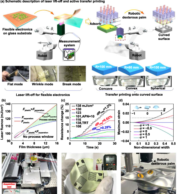
Figure 3. Digital, conformal transfer printing process for flexible electronics from a 2D planar substrate to a 3D curved surface. (a) A schematic depiction of robotized LLO and transfer printing techniques. Reproduced with permission from [38, 41]. Copyright 2018, Springer Nature. Copyright 2020, Elsevier. (b) The process window for laser fluence and film thickness. Reproduced with permission from [42]. Copyright 2020, Elsevier. (c) Statistics from the LLO process by real-time monitoring. Reproduced with permission from [42]. Copyright 2020, Elsevier. (d) Strain and strain energy during conformal contact: maximum strain in island with nondimensional width κ2wisland at κ2tisland = 10∼6. (e) The physical picture of real-time monitoring of robotized LLO process. (f) A flexible strain sensor prepared by LLO. Reproduced with permission from [38]. Copyright 2018, Springer Nature. (g) The dexterous robotic palm and the transferred flexible sensors on a curved surface.
Download figure:
Standard image High-resolution imageLLO systems are used to delaminate flexible electronics from a transparent substrate. The home-made LLO platform (LaserPeeler α1) is equipped with a pulsed laser (XeCl excimer laser, wavelength of 308 nm, OptoSystems CL7020). The laser beam is shaped into a narrow rectangle (20 × 0.62 mm) by the shaping lens. The laser beam passes through the attenuator to adjust the output energy of the laser beam (10%–90%). Uniformity of the laser beam is higher than ±5% after using a homogenizer. Due to the melting, vaporizing, or dissociating of the sacrificial layer (e.g. PI and PZT) at the interface, the LLO process can peel the rigid chips or flexible electronics off of the sapphire substrate [42]. However, there are three kinds of lift-off results for ultra-thin flexible electronics: flat mode, wrinkling mode, and break mode. Collaborative optimization is critical in order to safely peel off flexible electronics from their donor substrates without mechanical deformations, wrinkles, or cracks [43]. As the thickness of flexible electronics gradually decreases, the nondestructive peeling of ultra-thin flexible electronics is a great challenge in the LLO process. The main reason is that the process window for laser fluence is significantly reduced with the film thickness decreases (figure 3(b) [42]). The theoretical ultimate thickness is ∼5 μm. Meanwhile, the real-time monitoring of the LLO process is adopted via the feedback signals of ultra-thin flexible sensors on the PI substrate. The experimental results verify the feasibility and effectiveness of the active deformation model and process. In figure 3(e), the flexible strain sensor that was prepared on a 2 μm-thick PI film (figure 3(f) [38]) and connected to the digital multimeter was utilized to capture the plastic deformation during the LLO processes in real-time. As shown in figure 3(c), the step-like measured resistance reflects the frequency of laser irradiations and the impact on the ultra-thin flexible electronics [42]. In summary, LLO can delaminate various kinds of devices (e.g. rigid chips and flexible electronics) through reshaping the laser spot and adjusting the energy density.
To achieve successful peeling-off of thinner flexible electronics, the optimization strategy combines the accumulated pulse number and laser energy. By using the optimal process strategy and real-time monitoring of the LLO process, the strain sensor was released from the glass substrate without any damage or wrinkling in the laser fluence of 93 mJ cm−2, the accumulated pulse number was 10 and the variation in resistance was less than 5%. According to the conformal principle, a series of ultra-thin flexible electronics with specific thicknesses or sizes were successfully transferred to the curved surface, as shown in figure 3(g) [44, 45]. Additionally, we propose an LLO method to fabricate lead zirconate titanate (PZT) piezoelectric sensors, which commonly undergo high-temperature (∼650 °C) annealing processes directly on flexible substrates, such as PI (∼300 °C), polyethylene terephthalate (∼120 °C), and polydimethylsiloxane (∼150 °C). Finally, a PZT-integrated, bilateral multimodal sensor on a flexible substrate was fabricated. This flexible sensor was utilized to perceive the dynamic pressure and temperature stimuli.
The dexterous robotic palm, which can deform actively and digitally, is an executive device of conformal transfer printing. It was utilized to place flexible electronics on a curved surface via a motor array that can deform to the shape of the curved surface. The dexterous robotic palm consists of three parts: an adaptive stamp driven by motor arrays (e.g. 3 × 3), an air chamber with tunable negative/positive pressure, and a permeable elastic membrane to hold flexible electronics. The flexible electronics are picked up from the flat substrate via vacuum or electrostatic adsorption. Then, the flexible electronics are deformed towards the target surface via the dexterous robotic palm (active deformation process). The practical deformation, which is the same as the target surface, is based on the minimization of the elastic potential energy of the flexible electronics and the permeable elastic membrane. Depending on the positive pressure in the dexterous palm, the flexible electronics are placed and compressed onto the various target curved surfaces, such as concave, convex, and spherical curved surfaces, shown in figure 3(a).
Meanwhile, it is a challenge to conformally mount a nonstretchable device on a rigid, nondevelopable surface. The maximum strain in flexible electronics can be predicted by the scaling law:  max = f(α, k2, wisland, tisland), as shown in figure 3(d) [44, 46]. The corresponding size must be carried out according to the scaling law, where α= k1/k2 is a geometric parameter, k1 and k2 are the two principal curvatures, ξ = γ/(Eisland
tisland2
critical) is a non-dimensional parameter, ξcritical = 1/[2(1−v2
island)] is a constant, γ is the interface adhesion energy per area unit, Eisland and visland, tisland is the Young modulus, Poisson ratio, and thickness, respectively, and critical is the critical failure strain. It shows that the maximum strain max has different trends with the α and k2
wisland. When α < 0, the surfaces become convex. The maximum strain may exceed the failure strain of 1% for most of the inorganic materials. When α ⩾ 0, the surfaces become concave. As a result, compressing strain appears, which may cause island buckling or failure.
max = f(α, k2, wisland, tisland), as shown in figure 3(d) [44, 46]. The corresponding size must be carried out according to the scaling law, where α= k1/k2 is a geometric parameter, k1 and k2 are the two principal curvatures, ξ = γ/(Eisland
tisland2
critical) is a non-dimensional parameter, ξcritical = 1/[2(1−v2
island)] is a constant, γ is the interface adhesion energy per area unit, Eisland and visland, tisland is the Young modulus, Poisson ratio, and thickness, respectively, and critical is the critical failure strain. It shows that the maximum strain max has different trends with the α and k2
wisland. When α < 0, the surfaces become convex. The maximum strain may exceed the failure strain of 1% for most of the inorganic materials. When α ⩾ 0, the surfaces become concave. As a result, compressing strain appears, which may cause island buckling or failure.
3.3. Multimode EHD printing for various high-resolution microstructures
Conformal printing offers an attractive alternative to form functional electronic circuitry, components, and sensors directly on flexible or curved surfaces. The digital, noncontact process enables traces to be printed conformally on nonplanar objects while simply depositing and patterning of functional materials in a print-on-demand manner. Generally, it comprises three sub-steps to establish an electronic device on a curved surface: pattern designing, conformal printing, and sintering solidifying, as shown in figure 4(a). High-resolution patterns across large areas are a long-term challenge for printing techniques. Additionally, droplet flow is inevitable on nonplanar surfaces, so an ink that is compatible with high viscosity (e.g. silver paste) and high solid content are required. Access to the fabrication of multi-structure, such as dots, lines, or films, is appealing for different printing demands.
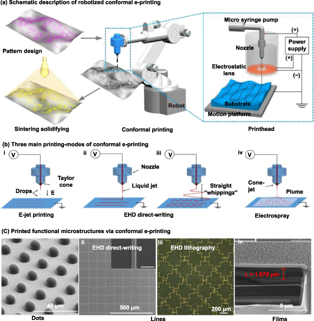
Figure 4. Multimode robotized EHD printing for various microstructures. (a) Schematic description of conformal EHD printing for curved electronics with a home-made electrostatic lens-integrated printhead. Reproduced with permission from [48]. Copyright 2019, Institute of Physics Publishing. (b) Three types of conformal EHD printing modes. (c) Four main kinds of structures printed by the strategies of conformal EHD printing. Reproduced with permission from [21, 37] Copyright 2020, Elsevier. Copyright 2018, John Wiley and Sons.
Download figure:
Standard image High-resolution imageThe EHD printing adopts electrical force to pull the jet from the nozzle, rather than pushing it through a resistive heater or piezoelectric transducer as in traditional inkjet printing [47]. When a proper electrical field is employed to the extraction electrode at the outlet of a nozzle, a tiny liquid droplet with a stable hemispherical liquid cone at the tip of the capillary forms as the balance of the gravity force, surface tension force, and electric field force. When the critical potential is reached, the repulsive electrical forces overcome the surface tension forces, and the liquid cone distorts into a 'Taylor cone,' and a charged jet will be ejected from the tip of the Taylor cone [29]. Unfortunately, the alteration in curvature of nonplanar substrates or standoff height during the printing process may affect the uniformity of the applied electric field, and this may impair the uniformity and stability and even lead to printing failure. To fully eliminate the applied voltage between the printhead and substrate, an electrostatic lens has been designed and integrated into the EHD printhead, as shown in figure 4(a) [48]. The electrostatic lens can generate electrostatic focusing to drive a Taylor cone to generate jetting without voltage or with small voltage being applied between the printhead and the substrate. It prevents the standoff height from influencing the nonplanar substrate or the initiating voltage and prevents the charge repulsion from polarizing the insulating substrate. The newly proposed printhead has been successfully applied to print complex patterns on both insulating and curvilinear substrates. It led to EHD printing on an arbitrary substrate in a direct, precise, and low-voltage manner. The electrostatic lens-integrated printhead thoroughly breaks the restrictions of printing on insulating and nonplanar substrates and significantly broadens its applications.
EHD printing is totally different from the traditional inkjet printing in the aspect of ink compatibility, resolution, and printing modes. Firstly, the EHD printing technique exhibits superior compatibility for ink with high viscosity (1–10 000 cps), which breaks the limits of ink viscosity (∼5–20 cps) of traditional inkjet printing. Various solutions, such as polymer solution, silver paste, and even molten liquid, can be printed directly, which is helpful for surpassing the limitations of ink for high-performance devices. Additionally, this technique significantly weakens the influence of ink flow on a nonplanar surface. Secondly, the resolution of EHD printing can reach 100 nm that is two orders of magnitude higher than that of inkjet printing. The main reason for this outcome originates from the shear deformation of the gas–liquid interface of the Taylor cone in the electric filed, rather than the solid-liquid interface of inkjet printing. The diameter of the jet is not limited by the inner diameter and can be as small as ∼1/1000 of the nozzle [49]. By carefully adjusting the ink parameters (e.g. viscosity, surface-tension, and conductivity) and printing parameters (e.g. offset height, pulse duration, potential difference, flux, or motion speed), the printing resolution can be well tuned from tens of micrometers down to tens of nanometers. Finally, three types of EHD printing modes can be realized, namely EHD jet printing (drop-on-demand) for small dots [50], EHD direct-writing for fine lines [29], and electrospray for nanoscale thin films [51], as shown in figure 4(b). From the points of ultrahigh resolution, excellent ink compatibility and versatile printing modes, EHD printing exhibits many more advantages and overcomes the limits of inkjet printing.
This technique has been widely utilized to fabricate dots, lines, and films, as shown in figure 4(c), which are the building blocks of electronic devices. Drop-on-demand EHD jet printing is capable of fabricating dot arrays with resolutions from 0.1 μm to 100 μm and various morphologies ranging from thin films to thick structures on flexible and curved substrates (figure 4(c-i) [37]). Continuous EHD direct-writing enables the fabrication of both straight and serpentine conductive interconnects on 2D planar and 3D curved surfaces. Particularly, the serpentine pattern is formed by the rotation of jetting and the straight motion of the robot system. These advantages free the printing process from the influence of the positioning accuracy of the robot-like system (figures 4(c-ii) and (c-iii) [21]). Furthermore, it can create photoresist patterns on a curved surface for lithography, namely conformal EHD lithography [21], and it breaks the limits of established photolithography on curved surfaces to prevent patterning photoresist via a physical mask. Metal-network electrodes have been successfully fabricated on a 1.2 μm-thick, planar PET substrate as a touch screen and on a curved glass substrate as a conformal heater. Furthermore, electrospraying is utilized to deposit highly uniform nanofilms for 2D planar and 3D curved electronics, such as thin film encapsulation for organic light-emitting devices (figure 4(c-iv)) To improve uniformity, a 5/6-axial motion stage was adopted to guarantee EHD printing in a perpendicular manner.
3.4. Versatile microplasma jetting for selective surface preparation
Additionally, a group of fabricating procedures, such as etching, surface modification, doping, and nano-welding, are required to fabricate curved electronics, especially in a digital, noncontact, and selective manner. Examples of these procedures include engineering surface wettability ahead of EHD printing, selective etching for patterning microstructures, and assembling robust conducting nanofibers/nanowires network via nano-welding, which are quite common procedures. More importantly, this process shares the control system and end effector (e.g. printhead system) with other processes as much as it can.
Plasma treatment is a key enabling technology for microfine cleaning and surface modification, especially in the microelectronics industry. Nevertheless, traditional plasma treatments are usually carried out in a vacuum system, and the patterning procedure is commonly finished via a physical mask. It is not compatible with the fabrication of curved electronics in ambiences. An atmospheric-pressure, room-temperature plasma jet can enable high-efficiency surface modification via chemical functionalization or reactive etching [27, 30, 52, 53], only by scanning the plasma jet over the specific surfaces under ambient conditions, as shown in figure 5(a-i). This plasma does not require a vacuum system or high temperature conditions, and by tuning the diameter of the plasma jet, the spatial resolution can be easily controlled from >1 mm down to ∼10 μm. By simply substituting the printhead mentioned above for the tubular generator of the plasma jet, one can realize versatile plasma treatment in ambient conditions on arbitrary curved surfaces using the same apparatus (figure 5(a-ii)), including surface modification or patterning via mildly or severely discharging helium with a desirable amount of oxygen gas mixture, respectively; chemical doping by mixing gaseous dopants into the helium carrier gas; and cold welding by adopting pure helium working gas. These additional functions would no doubt expand the manufacturing horizon of the newly developed equipment. Thus, it is highly desirable to integrate the flexible plasma processes into the robotized hybrid printing system.
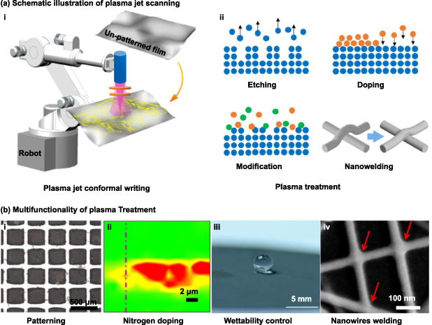
Figure 5. Robotized plasma jet direct writing/scanning for selective surface preparation. (a) Schematic description of conformal plasma jet treatment, including etching, doping, modification, and nanowelding. (b) Four main modes of plasma operation strategies and functions, including patterning, nitrogen doping, wettability control, and nanowire welding. Reproduced with permission from [27, 30, 39, 53] Copyright 2014, AIP Publishing. Copyright 2017, Elsevier. Copyright 2020, Elsevier. Copyright 2017, IOP Publishing.
Download figure:
Standard image High-resolution imageSince it combines chemical modification and reactive etching as a whole when processing, the features of the multifunctional plasma jet make it applicable to the fabrication of a variety of micro/nanostructures, such as patterning, nitrogen doping, wettability control, and nanowire welding, as shown in figure 5(b). Firstly, plasma jetting has been utilized to pattern etch preformed carbon nanotube (CNT) films (figure 5(b-i) [53]) to fabricate high-performance all-solid-state flexible micro-supercapacitors. Secondly, this technique enables site-selective functions in 2D materials. It has been successfully utilized for nitrogen doping of graphene (a single layer atom in thickness) with high spatial resolution of 10 μm without deteriorating the surrounding nanostructures (figure 5(b-ii) [27]). Thirdly, it can modulate the surface wettability that is a key factor for the following inkjet printing. In addition, plasma micro/nanotexturing can form hierarchical surfaces and newly functionalized oxygen-containing groups on stretchable CNTs/polydimethyl-siloxane (PDMS) films (figure 5(b-iii) [30]). Superwettable CNTs/PDMS films/patterns that combine robust stretchable super hydrophobicity and electrical conductivity have been applied successfully in corrosion-resistant epidermal sensors, water droplet manipulation, and in-plane microfluidic. Finally, microplasma jet processing endows the rapid cold nano-welding of conductive polymer nanofibers or silver nanowires (figure 5(b-iv) [39, 54]) without altering the morphology, nanostructure of the as-prepared film while significantly improving the electrical and mechanical properties. The optical transmittance is left nearly unchanged. These results indicate that an atmospheric-pressure, room-temperature plasma jet is a versatile process and has a powerful capability to realize the conformal fabrication of micro/nanostructures. When combined with the robotized hybrid printing equipment, the manufacturing scope will no doubt expand tremendously.
4. Robotized 'transfer-and-jet' printing of typical curved electronics
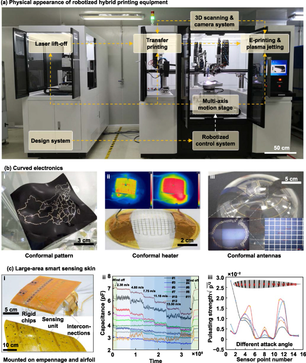
The robotized system can efficiently integrate multiple essential processes, such as transfer printing, EHD printing, and plasma direct writing. Figure 6(a) shows the appearance and basic components of a robotized hybrid printing equipment, including an LLO module and a home-made dexterous robotic palm for conformal transfer printing, a home-made electrostatic focusing printhead for conformal EHD printing, a 3D laser measurement and machine vision module for global and local positioning, and a plasma jet processor for pre/post-treatment. By the full combination of a 3D laser scanner and a 3-axis linkage motion system, the equipment enables the surface reconstruction, global positioning, and error detection of arbitrary curved substrates. It can automatically fit onto a large curved electronic system with the superiority of high precision, high efficiency, and high automation. A large curved electronic can be successfully fabricated by employing necessary modules in sequence. Firstly, the 3D models of curved substrates are acquired through the 3D scanning module. Next, the designed circuits are imported and projected to the 3D models through the design system. Then, different process modules are chosen, permutated, and combined according to the requirements. Meanwhile, the motion planning, on-line monitoring functions are carried out through the robot-like system. Different permutations and combinations of the processes are adopted for various applications.
Figure 6. Robotized hybrid printing equipment and its applications. (a) Photograph of the self-developed, robotized hybrid printing equipment that integrates a design system, robotized control system, 3D scanner, machine vision, multi-axis motion stage, LLO, transfer printing, EHD printing, plasma jetting, etc. (b) Applications of curved electronics fabricated by robotized hybrid manufacturing equipment. (c) The large-area smart sensing skin mounted on an empennage and a standard airfoil NACA0012 wing, the surface pressure under different wind velocities, and the pulsating pressure with different AOAs.
Download figure:
Standard image High-resolution image
Several functional circuits have been successfully fabricated, as shown in figure 6(b), including conformal conductive interconnectors, heaters, and antennas. These curved units are generally fabricated by two typical modes of EHD printing, namely additive EHD direct-writing or subtractive EHD lithography. Specifically, a flexible curved map of China was successfully printed onto the surface of a thin (∼50 μm) plastic film supported by a curved substrate, as shown in figure 6(b-i). The procedure of the corresponding fabrication consists of five major techniques, including 3D scanning, plasma treatment, conformal transferring, conformal printing, and photon sintering. Firstly, 3D scanning is adopted to establish a 3D point cloud of the curved substrate. Then, the geometric error calibration and the trajectory planning is formed by incorporating the designed CAD model. Secondly, the polymeric solution, such as polyvinyl alcohol, is deposited on the surface of the curved substrate as a sacrificial layer by the electrospraying process. Thirdly, a thermoplastic film is conformally transferred and pasted onto the surface in a high-temperature environment. Fourthly, plasma treatment is adopted to tune the surface wettability and enhance the interface adhesiveness. Finally, the high-viscosity silver paste is printed to form the desired patterns. The width of the printed traces is kept from a few to hundreds of micrometers, and more importantly the continuity of the conductive structures is determined by the EHD direct-writing process rather than the precision of the robot-like motion stage.
Alternatively, the EHD lithography that adopts the EHD printing technique to directly form conformal patterns of photoresists for wet lithography is presented, which breaks the limits of photolithography on curved surfaces. A conformal heater and a conformal antenna are taken as examples of EHD lithography, as shown in figures 6(b-ii) and (b-iii). Firstly, the plasma is utilized to clean and modify the curved glass substrate. Secondly, a conductive Cu or Au thin film is deposited onto the curved surface via magnetron sputtering, vacuum evaporation, etc. Thirdly, specific patterns of photoresists or other polymeric materials are created on the conductive film by conformal EHD printing (e.g. e-jet printing or EHD direct-writing). After exposure to wet chemical etching, the circuit forms on the curved substrate, accordingly. It is a mask-free photolithography and does not require the exposure or development necessary for photolithography. A 3D curved heater was fabricated on transparent glass. The nephogram of temperature suggests that the heater works well and its temperature distribution is rather uniform [21]. Similarly, a conformal electrically small antenna is also fabricated on a concave hemispherical surface in the form of conductive meandering lines. It needs to be emphasized that the patterned film consists of a 10 μm-wide metal mesh. Since the EHD printing technique holds the advantage of high-resolution patterning, it can enable the fabrication of transparent electrodes on curved substrates.
Figure 6(c-i) show a large-area, flexible smart sensing skin that is mounted on an empennage (over 30 × 50 cm size) and the curved surface of a NACA0012 airfoil model (15 × 15 cm) as a typical flexible hybrid electronic. The basic unit consists of one rigid capacitive-digital conversion chip, an array of detecting and calibration sensors including 15 flexible piezoelectric sensors that detect pulsating pressure, 14 flexible capacitive sensors that measure static pressure, five flexible resistive sensors to measure temperature and strain, and large-scale conductive circuits to connect these devices to the data acquisition system. The transfer printing is adopted to peel off rigid chips and flexible sensors from the planar substrate by the LLO process. Then, the dexterous robotic palm picks them up and conformally places them onto a desirable site on the target curved surface. The electrical connection is realized by printed-circuit-broad techniques or conformal EHD printing with laser sintering. From the output of the capacitive sensors at the fixed angle of attack (AOA), one can observe that the static pressure drops continuously with time as the wind speed increases, as shown in figure 6(c-ii). For a positive AOA (15°), the pressure drops sharply in the leading edge of the wing and becomes negative, as shown in figure 6(c-iii). The pressure remains stable in the middle of the airfoil and gradually increases at the trailing edge. Furthermore, the pulsating pressure rises sharply at the trailing edge from the output of the piezoelectric sensors distributed on the airfoil cord, indicating that an air separation point occurred at an AOA of 15°.
5. Conclusions
This work presents a robotized 'transfer-and-jet' printing technique to assemble diverse electronic devices on 3D curved surfaces. The newly proposed technique holds the unique capability to integrate rigid chips, flexible sensors, and conformal circuits. The involved processes, including transfer printing, inkjet printing, plasma scanning, and other auxiliary processes, are digitalized and combined by programmable robotization techniques, such as surface reconstruction and localization, path programming, and motion stages. The permutation and combination of these processes achieves versatile conformal fabrication. Specifically, a conformal heater and antenna on spherical surfaces and a flexible smart sensing skin on a winged model were successfully fabricated. The results prove that robotized hybrid printing can overcome the fundamental constraints of 2D planar microfabrication technologies and become powerful for 3D curved electronics.
The robotized hybrid printing equipment is a robot-like system that integrates measuring, planning, and execution systems to monitor states of printing, circuits, and tools. This system autonomically controls its components via measurement data and process knowledge. This endows the robotized printing system with high flexibility and compliance, and it is suitable for fabricating nonstretchable, large-area structures on highly complex surfaces. Its in-situ integration features can significantly reduce residual stress. Therefore, it brings about technological revolution, from 'small-area' to 'large-area,' from 'planar' to 'curved,' from 'rigid' to 'flexible,' and from merely additive printing or subtractive lithography process to hybrid processes. Although robotized hybrid printing shows great potential in large-area, multifunctional, curved electronic systems with distributed sensors, circuit, and actuators, there are still many challenges in the fabrication process, such as manufacturing multi-scale or multi-layered structures, increased efficiency, and integrated functionality. Future efforts should concentrate on improving the manufacturing precision of the entire robotized 'transfer-and-jet' printing and the intelligent and flexible coordination between each process and technology.
Acknowledgments
The authors acknowledge support from the National Natural Science Foundation of China (51635007, 51925503, 51705179), Natural Science Foundation of Hubei Province of China (2020CFA028). The general characterization facilities are provided by the Comprehensive Experiment Center for Advanced Manufacturing Equipment and Technology at Huazhong University of Science and Technology.