Abstract
The performance of state-of-the-art superconducting quantum devices is currently limited by microwave dielectric loss at different interfaces. α-tantalum is a superconductor that has proven effective in reducing dielectric loss and improving device performance due to its thin low-loss oxide. Here, we demonstrate the fabrication of high-quality factor α-tantalum coplanar-waveguide resonators directly on pristine 300 mm silicon wafers over a variety of metal deposition conditions and perform a comprehensive material and electrical characterization study. Additionally, we apply a surface treatment based on hydrofluoric acid that allows us to modify different resonators surfaces, leading to a reduction in two-level system loss in the devices by a factor of three. This loss reduction can be entirely attributed to the removal of surface oxides. Our study indicates that large scale manufacturing of low-loss superconducting circuits should indeed be feasible and suggests a viable avenue to materials-driven advancements in superconducting circuit performance.
Export citation and abstract BibTeX RIS

Original content from this work may be used under the terms of the Creative Commons Attribution 4.0 license. Any further distribution of this work must maintain attribution to the author(s) and the title of the work, journal citation and DOI.
1. Introduction
Increasing qubit coherence time is essential for enhancing the capabilities of noisy intermediate-scale quantum processors, and crucial for reducing the error-correction overhead in future fault-tolerant quantum computers [1, 2]. Historically, several approaches have been explored to increase their performance such as, participation ratio engineering [3]âtypically resulting in bigger qubits- as well as optimal control [4, 5], shielding [6] and signal filtering [7]. In contrast, the number of advancements based on understanding microscopic origin of decoherence and energy lossâincluding the judicious increase of the materials toolboxâis rather limited [8, 9], with most published work focusing on only a few well documented materials such as Al [10â15], Nb [16â20], TiN [21, 22], NbN [23, 24], NbTiN [25â27], granular-Al [28, 29], Re [30] and In [31]. Only recently, the suite of materials for superconducting quantum technology was further expanded, markedly resulting in qubit relaxation times as high as 0.5 ms for 2D transmon qubits by using α-tantalum (α-Ta) [32, 33]. It has been suggested that the simpler native oxide structure of tantalum [34, 35] compared to native oxide structures of other materials such as niobium (Nb) [36] leads to lower microwave loss. However, these studies employed sapphire as substrate, which has lower dielectric loss [37â39] than the high-resistivity silicon (Si) substrates [40, 41] typically used in superconducting circuits, potentially positively affecting the obtained relaxation times. Moreover, the use of sapphire substrates is incompatible with fabrication processes and requirements needed to manufacture and integrate large numbers of qubits in 300 mm industry-scale facilities. While the deposition of α-Ta directly on thermally oxidized Si [42] substrates has been known since the 90s, it is widely recognized that the silicon oxide at the siliconâtantalum interface has a detrimental effect on the performance of superconducting qubits and resonators. To circumvent the issue, α-Ta coplanar-waveguide resonators, which are short loop proxies for superconducting qubits, have been fabricated with the help of seed layers such as Nb [43, 44], tantalum nitride (TaN) [45], and titanium nitride (TiN) [46]. Nonetheless, this approach adds to the processing complexity during both the deposition and etching stages of the metallic layers. Furthermore, it introduces an additional interface that could potentially harbor additional two-level system (TLS) defects [47], thereby potentially compromising the performance of the superconducting device. Recently,
LC α-Ta resonators have been deposited on pristine Si at elevated temperature [48]. However, due to unspecified design parameters and a frequency range not typically used for superconducting qubits, these results are difficult to compare to the other works and make it hard to judge the relevance of high-temperature fabrication processes for high-coherence quantum computing applications.
In this study, we demonstrate the fabrication of high-Q factor α-Ta coplanar-waveguide resonators on pristine 300 mm Si substrates over a wide temperature processing window that allows the growth of α-Ta films with different crystallographic texture and resistivity values. We characterize the microwave performance of the devices and show that our results are consistent with TLS-induced dissipation. We further implement and perform in-depth characterization of the metal-air (M-A), metal-substrate (M-S), and substrate-air (S-A) interfaces by combining spectroscopy and microscopy techniques to locate loss sources. Finally, by applying a surface treatment based on hydrofluoric acid (HF) we mitigate the TLS loss by a factor of three, reaching internal Q-factors as high as 4.5â 106 at single photon powers and demonstrate that this loss reduction is associated to surface oxide removal.
2. Characterization of α-tantalum films
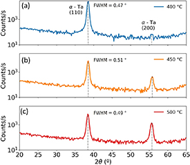
We sputter α-Ta films on HF-cleaned Si substrates at 400 °C, 450 °C and 500 °C [49] with a nominal thickness of 100 nm. To verify the growth of the correct phase, we measure the x-ray-diffraction (XRD) spectrum of each film. Two diffraction peaks (figure 1(a)) corresponding to α-Ta are visible, indicating the polycrystalline nature of our films, while peaks corresponding to β-Ta are not present. We also observe that the height of the (200) peak increases as a function of deposition temperature, indicating that each of the films have a different crystallographic texture. To further confirm the growth of the α-Ta phase, we also perform electrical characterization of the films by measuring electrical resistivity across the 300 mm wafers (figures 2(a)â(c)). Room temperature resistivity is a good probe to test the tantalum phase formation since β-Ta exhibits resistivity values around 150 μΩ cmâ200 μΩ cm which is ten times higher than resistivity of the α-Ta phase 15 μΩ cmâ20 μΩ cm [50]. Room-temperature resistivity of the three films is comparable to the typical resistivity of α-Ta films with similar thicknesses [51] and it only slightly increases as a function of deposition temperature. Furthermore, low variability of the resistivity across each wafer of less than 3% indicates the formation of purely the α-Ta phase without the presence of minority β-Ta phase patches [52]. The observed increase in resistivity across the various α-Ta films can be attributed to a increment in grain boundary density, resulting from both the reduction in grain size as the deposition temperature increases, shown by the increase in the full width at half maximum of the (110) peak, and the concurrent increase in number grains along the (200) orientation [53]. In order to electrically validate and investigate the respective deposition conditions and to study microwave loss sources and potential microwave loss differences between the three film types, we pattern coplanar-waveguide resonators using the 400 °C, 450 °C and 500 °C α-Ta films. Resonator fabrication is performed in a 300 mm fabrication facility using industry-standard fabrication processes involving subtractive (dry) etching similar to previous reports [54].
Figure 1. XRD spectra of the 400 °C (a), 450 °C (b) and 500 °C (c) α-Ta films used for resonator fabrication.
Download figure:
Standard image High-resolution imageFigure 2. Resistivity maps of the 400 °C (a), 450 °C (b) and 500 °C (c) α-Ta films used for resonator fabrication.
Download figure:
Standard image High-resolution image3. Resonator microwave characterization
We characterize the performance of the superconducting quarter-wave coplanar waveguide resonators by performing S21 transmission spectrum measurements at 10 mK. All eight resonators on a chip are fed by a common transmission line and have a 4.5 µm wide gap and 10 µm wide central trace, while their frequencies are distributed between 4 and 8 GHz by appropriately adjusting their length. A fitting routine [55] is used to extract the resonant frequency, fr, internal quality factor Qi, and coupling quality factor Qc as a function of the estimated mean photon number in the different resonators investigated.
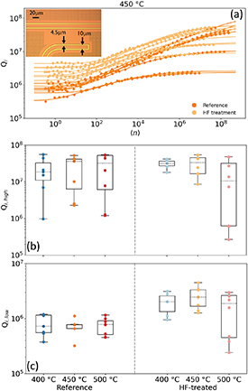
The resonators labeled as 'reference' correspond to as fabricated resonators without any post-processing, and the ones labeled as 'HF-treated' correspond to resonators that received a post-processing HF clean step not longer than 12 h before the packaging and cooling down in the dilution refrigerator. Apart from sample mounting and wire bonding, HF-treated resonators were stored in a N2 atmosphere during the 12 h waiting period. The HF post-processing treatment is employed in an attempt to reduce surface oxides, which are the major source of loss in superconducting quantum devices [56]. We used the same treatment as previously applied to Nb lumped element resonators (60 s in 5.5% HF) that were reported by Verjauw et al [36] since it has proven effective to completely remove SiOx , passivate the Si surface, as well as remove surface niobium oxides, resulting in a Qi increase by a factor of seven. In total, six different α-Ta chips (three reference chips and three HF-treated chips) were fabricated using the 400 °C, 450 °C and 500 °C α-Ta films. In both reference and HF-treated resonators, the observed Qi power dependence (figure 3(a)) indicates the presence of dominating TLS depolarization in our devices which is suppressed (saturated) at high photon powers [57]. In the high photon number regime (Qi,high) the reference and HF-treated resonators measured (figure 3(b)) exhibit Qi,high values up to 55â 106. As expected, the HF-treated resonators did not show much difference compared to the reference resonators in this high-power regime, in line with the hypothesis that surface related TLS losses are suppressed (saturated) in this regime and reducing the TLS density therefore has negligible effect. The behavior is different for low power Qi's (Qi,low), where no such saturation of loss takes place. The measured reference resonators have values ranging from 0.3â 106 to 1.2â 106. After the HF treatment, the Qi,low values increase (figure 3(c)) and vary between 0.2â 106 and 4.5â 106. The larger spread observed in the Qi,high and Qi,low of the resonators patterned in the 500 °C HF-treated α-Ta films compared to the 400 °C and 450 °C HF-treated α-Ta films comes from three resonators that show little Qi dependence as a function of photon number (see supplemental figure S3), indicating that other dissipation mechanisms different from TLS dissipation, such as trapped vortices [58], dominate resonator loss. Besides the spread in the Qi values, the three types of α-Ta films do not show a significant Qi,high and Qi,low difference. Differences in Qi,low could have been anticipated based on the XRD and resistivity data due to the differences in grain boundary densities of the three α-Ta films since grain boundary dissipation has been identified as a relevant relaxation mechanisms in nominal identical qubits fabricated in different types of Nb films [16]. The fact that Qi,low does not scale with grain boundary density in our study can be explained by the fact that differences are too small or that loss from grain boundaries is not as relevant in α-Ta films as it is in Nb films.
Figure 3. (a) Internal quality factor (Qi) as a function of estimated mean photon number for reference and HF-treated resonators. Lines are fittings to equation (1). (b) and (c) Boxplot summary of Qi, high and Qi, low of the reference and HF-treated Ta resonators.
Download figure:
Standard image High-resolution image4. Resonator interface characterization
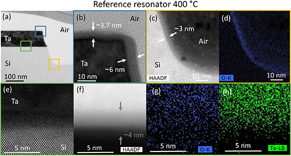
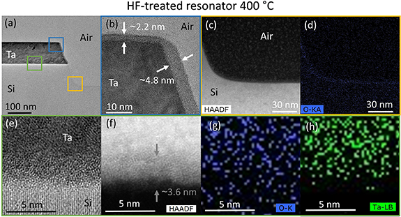
To investigate the increase in Qi,low after the surface treatment, we next study the morphology and composition of the M-A, M-S and S-A interfaces, regions that typically host dominant loss sources [59]. We conduct a detailed characterization of both reference (figure 4) and HF-treated (figure 5) resonators using scanning transmission electron microscopy (STEM) and energy-dispersive x-ray spectroscopy (EDS). All STEM images were taken no longer than 12 h after the HF treatment to mimic the conditions under which resonator Q-factors are measured. In the reference resonators, the top M-A interface (figure 4(b)) is covered by a 3.7 nm tantalum oxide layer, while the tantalum oxide at the side wall is about 6 nm thick. This difference arises from the oxygen plasma treatments [60] during the resonator fabrication and resonator cleaning processes. After the metal etch an oxygen plasma step is first applied to clean post etch residues. During this step the top metal surface is protected by a SiO2 hard mask, while the side walls are exposed to the plasma. Subsequently, the second oxygen plasma treatment is applied to clean individual chips once the protective resist for dicing has been removed. Since no SiO2 hard mask is present this time, oxide can grow on every surface. The S-A interface (figures 4(c) and (d)) contains approximately 3 nm thick SiOx and forms during the fabrication process, although the native SiOx was initially removed with the HF clean prior to Ta deposition. The M-S interface (figures 4(e) and (f)) is approximately 4 nm thick and consists of a mixture of Si and Ta, as shown by the contrast change in the high-angle annular dark-field-STEM image of the same region (figure 4(f)). This intermixing occurs due to the short-range diffusion of Si into Ta sputtered layers at elevated temperature [61, 62]. No oxygen can be detected above the background value in the M-S interface from the EDS map (figure 4(g)). The absence of a marked O signal across the Si-Ta interface implies negligible oxide growth in the time between the substrate HF clean and the metal deposition. Similar results are obtained also for 450 °C and 500 °C patterned Ta films (see supplementary figures S1 and S2 for STEM images of the resonators patterned using 450 °C and 500 °C α-Ta films). For the HF-treated resonators, the tantalum oxide thickness at the M-A interface (figure 5(b)) is reduced by 1.2â1.5 nm, while SiOx is completely removed on the S-A interface. The M-S interface is not exposed to the HF post-processing clean and is therefore not affected. The reduction of surface oxides at both the M-A and S-A interfaces likely explains the observed increase in Qi,low, as these oxides constitute significant sources of TLS.
Figure 4. STEM and EDS images of a 400 °C reference α-Ta resonator cross section. (a) Low magnification STEM cross section of Ta resonator. The colored squares mark the areas where high magnification images were taken. (b) STEM cross section of the M-A interface. Arrows indicate the tantalum oxide layer. (c) HAADF-STEM image of the S-A interface. The arrows indicate the silicon oxide layer present. (d) Oxygen EDS map of the S-A interface. (e) STEM image of the S-M interface. (f) HAADF-STEM image of the S-M interface. The arrows indicate the extension of the Si-Ta interfacial layer. (g) Oxygen EDS map of the S-A interface. (h) Tantalum EDS map of the S-A interface.
Download figure:
Standard image High-resolution imageFigure 5. STEM and EDS images of a 400 °C HF-treated α-Ta resonator cross section. (a) Low magnification STEM cross section of Ta resonator. The coloured squares mark the areas where high magnification images were taken. (b) STEM cross section of the M-A interface. Arrows indicate the tantalum oxide layer. (c) HAADF-STEM image of the S-A interface. (d) Oxygen EDS map of the S-A interface. (e) STEM image of the S-M interface. (f) HAADF-STEM image of the S-M interface. The arrows indicate the extension of the Si-Ta interfacial layer. (g) Oxygen EDS map of the S-A interface. (h) Tantalum EDS map of the S-A interface.
Download figure:
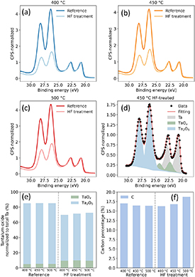
Standard image High-resolution imageFinally, x-ray photoelectron spectroscopy (XPS) is used to investigate the chemical composition of the M-A interface in both reference and HF-treated resonators. The doublet peaks situated at 21.6 eV (figures 6(a)â(c)) corresponds to metallic Ta, while the doublet peak situated at around 26.3 eV corresponds to tantalum pentoxide (Ta2O5). The similarities between these XPS spectra suggest that the film properties difference on texture and resistivity afore mentioned do not influence the tantalum oxide formation. By fitting the XPS signal (figure 6(d)), the atomic concentration of the different compounds at the M-A surface can be extracted. Ta2O5 is the main tantalum oxide detected, although a small percentage of tantalum suboxide (TaOx ) is also identified. The proportion of Ta2O5 and TaOx detected is similar in the 400 °C, 450 °C and 500 °C reference resonators. This is expected since the thickness of the top tantalum oxide layer in the three different films is comparable, as shown in the STEM images. After the HF treatment the total amount of tantalum oxides detected decreases between 15%â18%. This reduction is mostly due to the removal of Ta2O5 (figure 6(e)) since the amount of TaOx increases after the HF-treatment. These observations align with the measurements and modeling of tantalum oxide profiles presented by McLellan et al [63] where Ta2O5, the oxide closest to the surface, is the first to be removed during chemical treatment. Carbon peaks are also observed in the XPS spectra of the patterned M-A interface, which are also fitted to extract the C atomic concentration. The carbon (C) content is similar in all samples (figure 6(f)), except in the 500 °C HF-treated sample, where it is around 2% higher than the other films. This suggests that hydrocarbon residues might penetrate through grain boundaries deeper than 1 nm into the surface, since it is approximately the Ta2O5 thickness removed by the HF treatment.
Figure 6. (a)â(c) XPS spectra of a reference and HF-treated Ta chips fabricated using the 400 °C, 450 °C and 500 °C Ta films. (d) Fitting of the XPS spectra of a HF-treated chip fabricated using the 450 °C Ta film. Black dots are experimental data, red line is the fitting. The blue area represents the contribution to the fitting Ta2O5, the grey area corresponds to the contribution of metallic Ta, and the green area the contribution from TaOx . (e) Ta2O5 and TaOx percentage respect to the total amount of Ta detected in the reference and HF-treated resonators. (f) Percentage of C detected in the reference and HF-treated resonators.
Download figure:
Standard image High-resolution image5. Resonator modeling
To isolate material-specific TLS defect microwave loss we analyze Qi as a function of ãnã using the following standard model [53]:

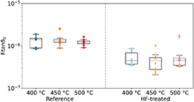
where F is the participation ratio, tanδ0 is the intrinsic loss tangent for the material containing the TLS and δother is the contribution from power independent non-TLS loss. Similarly, nc is the critical photon number equivalent to the saturation field of different TLSs and b is a phenomenological parameter, which is 0.5 for noninteracting TLS defects [64] and lower than 0.5 in the presence of TLS-TLS interactions [65]. Furthermore, h is the Planc constant, fr is resonator frequency, kB is Boltzmann constant and T is the temperature. Since measurements were performed at the base temperature of the dilution refrigerator (T = 10 mK), tanh factor is close to 1. Our data agrees well with the above model across all measured resonators (figure 4(a) and supplementary figures S3(a)â(c)). The extracted TLS loss, as expressed by Ftanδ0 (figure 7), is similar for the reference resonators in the three different α-Ta films with values ranging from 0.8â 10â6â1.9â 10â6. For the HF-treated samples, Ftanδ0 decreases displaying values within the range of 0.2â 10â6â1.7â 10â6, with median values decreasing by a factor of three when compared to the reference resonators. Like the previous analysis, there are no significant differences in Ftanδ0 among the three types of films utilized. This suggests that intrinsic film properties such as texture and resistivity do not currently limit the TLS loss. Regarding other fitting parameters, the b parameter is generally less than 0.5 (supplementary figure S4(b)), which aggress with previously b values reported [36] in resonators with Qi around and above 1â 106, indicating that TLS-TLS interactions are present. Critical photon numbers in α-Ta devices are found to be nc = 1â50, except for the HF-treated resonators fabricated with 400 °C α-Ta where nc can reach up to 150 photons (supplemental figure S4(c)).
Figure 7. Boxplot of the Ftanδ0 extracted from fitting the reference and HF-treated Ta resonators resonator data to equation (1). The boxes extend from the first quartile to the third quartile of Ftanδ0 with a line at the median. The whiskers extend from the box by 1.5 times the inter-quartile range.
Download figure:
Standard image High-resolution image6. Discussion
The observed reduction in TLS loss can be attributed primarily to a decrease in surface oxides, both at the M-A interface and the S-A interface. This reduction is evident in both the STEM images (figures 4(c) and (d), figures 5(c) and (d)) and the XPS analysis (figure 6(e)), where the amount of surface tantalum oxide decreases following the HF treatment, while the SiOx is completely removed, and no reoxidation is observed in the time before the measurement. Determining the impact of removing Ta2O5 on reducing TLS loss is challenging due to the concurrent increase in the amount of TaOx . It could happen that the dielectric loss of TaOx is greater than that of Ta2O5. As a result, a significant reduction in Ta2O5-related TLS loss may be offset by a slight increase in TaOx . In addition, the fact the carbon content in the reference and HF-treated resonators is similar indicates that the TLS loss contribution from hydrocarbon residues has to be smaller than the median TLS loss of approximately 0.45 â 10â6 in HF-treated samples which encompasses the TLS loss contribution from all interfaces and the substrate. These observations suggest that although the total dielectric loss in CPW resonators has different sources, surface oxides are still the main contribution in non-treated samples.
On average, the Qi,low values after the HF treatment obtained in this work are around 2â 106. These values are in the range of α-Ta CPW resonators of similar size reported on both Si [46] and sapphire [44, 48]. Transmon qubits made of α-Ta with record Qi of 7.1 â 106 and 11.8 â 106 have also been reported by Place et al [32] and Wang et al [33], respectively, while our record Qi,low is 4.5 â 106. However, due to differences in device geometry a direct quality factor comparison between qubits and resonators is difficult because of differences in the energy participation ratio of the interfaces. Another possibility for the quality factor difference is loss added by the M-S interface. In our samples no oxide is detected at the M-S interface (figure 4(h)), but there is evidence of Si diffusion into the Ta film (figures 4(e) and (f)), while in the α-Ta qubit samples reported in literature the M-S interface shows an atomically sharp boundary between Ta and sapphire [32]. Different tantalum silicide compounds are known to form at the Ta-Si interface when exposed to elevated temperatures. The formation of pentatantalum trisilicide (Ta5Si3) occurs when Ta films deposited on Si substrates are annealed at 550 °Câ600 °C for one hour [66], while tantalum silicide (TaSi2) requires temperatures around 785 °C [67]. These silicides are metallic [68, 69] and their presence at the M-S interface of superconducting devices might affect device performance. It is unlikely that these silicides are present at the M-S interface of our Ta resonator chips, since the maximum temperature used in the growth of these films is 500 °C, and all depositions were completed in less than ten minutes. As demonstrated by Cheng [62], the Ta-Si interfacial layer thickness can be controlled by modifying the annealing temperature or the annealing time. However, our STEM images indicate that the deposition temperature has no effect on the interfacial layer thickness (supplemental figures S1 and S2). Further investigations on the effect of the deposition time at elevated temperatures will be needed to conclude if the Ta-Si interfacial layer can be controlled and if this layer negatively affects device performance.
7. Conclusion
This study demonstrates the fabrication of superconducting high-quality α-Ta coplanar-waveguide resonators directly grown on pristine Si over a large temperature processing window. The combination of spectroscopy and microscopy enables us to investigate the composition and structure of the different resonator interfaces and to establish correlations with device loss. Our analysis shows that the removal of surface oxides leads to factor of three reduction of median TLS loss, while intrinsic film properties such as crystallinity and resistivity do not seem to play any role at the current loss level. Our work opens the possibility for integrating α-Ta as a low-loss material in the fabrication of larger and more complex superconducting devices, as well as making it compatible with fabrication in industrial-grade facilities. In addition, simulations [70, 71] of studied structures incorporating the material insight gained and the superconducting nature of the systems could contribute to the better understanding of the devices. The potential of this multidisciplinary approach to understand the material origin of loss sources paves the way to engineer high performance superconducting devices, as well as other quantum or classical technologies that benefit from low-loss superconducting materials such as trapped ions [72] microwave kinetic inductance detectors [73] single photon detectors [74, 75] and superconducting filters [76].
Acknowledgments
The authors gratefully thank Paola Favia, Olivier Richard, Chris Drijbooms, Ilse Hoflijk, Thierry Conard, Céline Noël, Valentina Spampinato, Alexis Franquet for metrology support. This work was supported in part by the imec Industrial Affiliation Program on Quantum Computing. We also thanks Nathalie de Leon for useful discussions and comments about this work.
Data availability statements
The data that support the findings of this study are openly available at the following URL/DOI: http://doi.org/10.5281/zenodo.10447511.
Funding
This project leading to this application has received funding from the ECSEL Joint Undertaking (JU) under Grant Agreement No. 101007322. The JU receives support from the European Union's Horizon 2020 research and innovation program and Germany, France, Belgium, Austria, Netherlands, Finland, Israel. (Please visit the project website www.matqu.eu for more information). This work was supported by imec's Industrial Affiliation Program on Quantum Computing.
Figure S1 (1.9 MB JPG) STEM 450 ºC resonator
Figure S2 (1.7 MB JPG) STEM 500 ºC resonator
Figure S3 (0.9 MB JPG) Qi versus photon number 400 ºC, 450 ºC and 500 ºC
Figure S4 (0.4 MB JPG) b, nc and ð other fitting parameter summary
Figure s5 (0.3 MB JPG) Cryostat measurement configuration
Supplementary data (3.3 MB DOCX) Supplementary material

