
Abstract
We present a magnetic tunnel junction (MTJ) based implementation of the spike time-dependent (STDP) learning for pattern recognition applications. The proposed hybrid scheme utilizes the spin–orbit torque (SOT) driven neuromorphic device-circuit co-design to demonstrate the Hebbian learning algorithm. The circuit implementation involves the (MTJ) device structure, with the domain wall motion in the free layer, acting as an artificial synapse. The post-spiking neuron behaviour is implemented using a low barrier MTJ. In both synapse and neuron, the switching is driven by the SOTs generated by the spin Hall effect in the heavy metal. A coupled model for the spin transport and switching characteristics in both devices is developed by adopting a modular approach to spintronics. The thermal effects in the synapse and neuron result in a stochastic but tuneable domain wall motion in the synapse and a superparamagnetic behaviour of in neuron MTJ. Using the device model, we study the dimensional parameter dependence of the switching delay and current to optimize the device dimensions. The optimized parameters corresponding to synapse and neuron are considered for the implementation of the Hebbian learning algorithm. Furthermore, cross-point architecture and STDP-based weight modulation scheme is used to demonstrate the pattern recognition capabilities by the proposed neuromorphic circuit.
Export citation and abstract BibTeX RIS

Original content from this work may be used under the terms of the Creative Commons Attribution 4.0 licence. Any further distribution of this work must maintain attribution to the author(s) and the title of the work, journal citation and DOI.
1. Introduction
Artificial intelligence and machine learning algorithms and tools have been investigated for efficient processing of the enormous amount of data piling up in today's world. The implementation of these data-intensive algorithms is based on the complementary metal-oxide memiconductor (CMOS) technology. As we get closer to the end of Moore's law and efficient scaling of transistors, the implementation of these machine learning algorithms using CMOS-based circuits has suffered from increasing dynamic and static energy dissipation [1], making them less energy efficient than the brain [2]. To address these problems, researchers are working at different levels of abstractions such as novel materials and devices [3, 4], and new architectures such as neuromorphic computing [5, 6]. The neuromorphic computing, which is inspired by the operation of the brain to tackle the Von-Neumann bottleneck [7], has gained a lot of interest in the research community. Both CMOS and beyond-CMOS devices are being used to implement artificial synapses and neurons [7, 8]. To realize the artificial synaptic device with the ability to remember the past state during computation, different types of memristors and phase change memories have been proposed [9], but most of these devices require high amplitude and long period voltage/current pulses to update their states [10], so they are not energy efficient. Novel spintronic devices, promising energy efficient storage and computation, are prime candidates as spin-memristors for neuromorphic computing [11, 12]. Particularly, due to its tuneable energy barrier the magnetic tunnel junction (MTJ) is being used in solving problems in deterministic and stochastic neuromorphic computing [13, 14]. In this work, we propose a MTJ-based device-circuit co-design to implement the spike time dependent plasticity (STDP) learning for pattern recognition applications [15]. The Hebbian learning algorithm implementation by the devices and the circuit is discussed. The cross-point architecture of these devices is used to demonstrate the STDP learning algorithm for pattern recognition applications. Moreover, we also discuss the dynamic learning capabilities of the circuit which reduce the energy dissipation in the subsequent training phases. The artificial spin-synapse considered in the circuit is an MTJ with the domain wall motion in the magnetic free layer (FL). The motion of the domain wall is driven by spin–orbit torque (SOT) at the FL/heavy metal interface. Motivated by the fast and stochastic switching in low barrier nano-magnets, we consider the realization of the post neuron using the low barrier MTJ switched by SOT. The spin-based implementation of both synapse and neuron, integrated on a single chip, as proposed in this work, promises significant reduction in the overall system complexity, total power, interconnect delay and overhead and the total chip area.
The rest of this paper is organized as follows. In section 2, we introduce the elements of our proposed spin-based neuromorphic computing system, such as: synapse, neuron, sensing, and weight modulating units. Section 3 is focused on the modeling of spin transport (non-equilibrium Green's function (NEGF) formalism) and micromagnetics in both neuron and synapse. The effects of the thermal noise on synapse and neuron are considered in the model. We use the model to discuss the thermal effects, the optimization of the switching delay and the writing current in terms of neuron and synapse dimensional parameters. Section 4 presents the circuit level implementation of the Hebbian learning algorithm. Based on the cross-point architecture of these devices we demonstrate the STDP learning for pattern recognition. We also evaluate the dynamic learning for pattern recognition capabilities of the circuit. Finally, in section 5, we conclude and propose future prospects of our work.
2. Neuromorphic device and circuit design
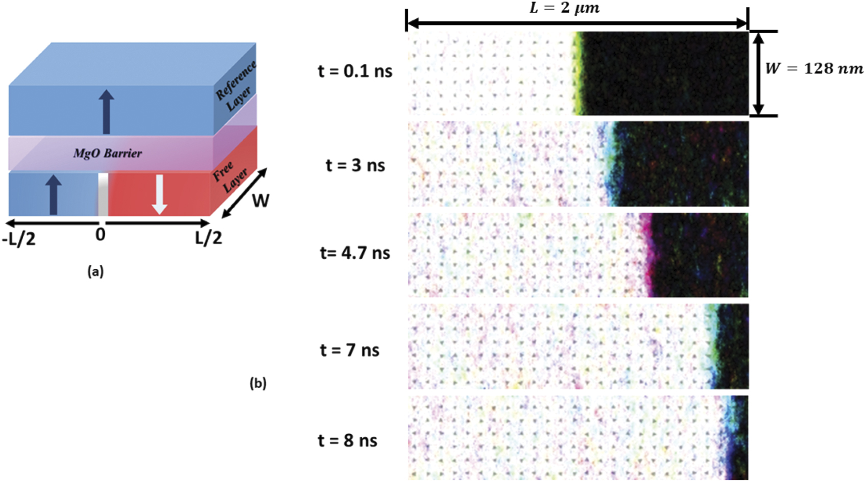
The schematic of the proposed system is shown in the figure 1(a). The connection between pre-neuron and post-neuron MTJs is mediated through a synapse MTJ with a transverse domain wall in the FL. The MTJ resistance varies with the change in the magnetization orientation between the free and fixed layers. The device is in a high resistance state for complete anti-parallel magnetization configuration between free and fixed layers, while the resistance in the parallel state is low. The difference between two extreme resistance states depends upon the tunnel magnetoresistance (TMR) of the device. The domain wall motion changes the overall magnetization of the FL gradually, which reflects in the gradual variation of MTJ resistance. Thus, we get analog synaptic weights in terms of these resistance values which are controlled by the spin Hall effect (SHE) generated SOT on the domain wall. The pre-neuron (terminal-1) signals pass through the domain wall 3T-MTJ synapse into the output (terminal-3). Terminal-3 is directly shorted to the input (heavy metal) of post-neuron MTJ and the drain of a refractory transistor at (terminal-4). Likewise, all other pre-neuron signals are connected to post-neuron input via their respective synapses in a simple feed-forward manner. The current coming from all the pre-neurons add up in the post-neuron heavy metal tungsten (β-W). The charge-spin conversion in the heavy metal generates a pure transverse spin current resulting in SOT on the FL magnetization. The post neuron FL magnetization is switched with the condition that pattern pixels as the pre-neuron signals generate current, which is above the switching threshold. The resistance switching in the post-neuron due to magnetization flipping reflects a sudden voltage spike (mV-range) generated at the output. The neuron output voltage readout unit (C) consists of an operational amplifier-based voltage comparator which compares this mV MTJ voltage with a reference voltage (Vref ) and generates a (V-range) binary output. The binary output of the comparator also turns on the transistor-T1 and turns off transistor-T2. This disconnects the post-neuron from the synapses temporarily and depending upon the correlation between the pre-neuron spike and the post-neuron spike synaptic weight update is carried out using update pulses from the weight update unit. The weight update unit consists of the CMOS switches receiving input from pre-neuron and post neuron as shown in figure 1(a). When both post-neuron and pre-neuron spikes are on simultaneously a positive current pulse flows through the synapse heavy metal from terminal -2 to terminal -3, terminal- 3 is grounded via T1. Thus, during the update phase the post neuron is not affected. Similarly, a negative current flow between terminal -2 and terminal -3 for negative or zero correlation. A positive update pulse between (terminal-2) and (terminal-3) moves the domain wall to the left, reducing the MTJ synaptic resistance. Whereas, the domain wall moves to the right for the negative current pulse, consequently increasing the resistance of the MTJ synapse. Figure 1(b) shows the 3D device structure depicting both synapse and neuron on a single wafer. The different synapses are separated from each other by an oxide barrier preventing the interference between different pre-neuron signals. The weighted current pulses are collected in the post-neuron heavy metal.

Figure 1. (a) Complete schematic of the neuromorphic system, showing the connection between pre-neuron, synapses, post-neuron, sensing and weight update circuitry (b) device design on a single chip for experimental implementation.
Download figure:
Standard image High-resolution image3. Modeling spin transport and magnetization dynamics in synapse and neuron
To model the spin transport and magnetization dynamics in synapse and neuron, we develop the NEGF coupled Micromagnetics model. The spin orbit torque control of the magnetization switching is included in terms of the extra spin orbit field terms in MuMax3 [16]. By adding thermal noise term in the model, we have carried out the study of the thermal effects on switching behavior of neuron and synapse.
3.1. Synapse model
The modeling of synaptic resistance evolution during the training phase is carried using spin transport computations by using effective mass tight binding (EMTB) for describing the MTJ device Hamiltonian and NEGF for the computation of current and resistance. The FL magnetization evolution in presence of SOT is computed by the micromagnetic tool MuMax3. The basic equation describing the magnetization dynamics is Landau–Lifshitz–Gilbert equation given by:

where effective magnetic field is

γ is the gyromagnetic ratio and α is the damping constant.
We add spin orbit torque in terms of the additional field term h SOT [17].

where, p is a unit vector in the direction of the magnetic moments that are injected into the ferromagnet, determined by

The magnetization acts as input to the NEGF module and correspondingly for every change in magnetization, we compute the time evolution of the resistance.
The side view of an MTJ with a domain wall in the FL is depicted in figure 2(a). Considering the position of the domain wall at (x), computed using micromagnetics model the synaptic resistance of the MTJ depends on the x and is computed analytically by:

where RP/RAP is the MTJ resistance state when the FL magnetization is completely parallel/anti-parallel to the fixed layer, x is the position of the domain wall and L is the length of the FL. The position of the domain wall is computed by:

where t1 − t2 is the synaptic update pulse width and VDW is the domain wall velocity expressed as [18].


where U, β, WDW, μB, P, MS, q, J are the domain wall velocity in presence of spin transfer torque, non-adiabaticity parameter, domain wall width, Bohr magneton, polarization, saturation magnetization, the electron charge and current density, respectively.

Figure 2. (a) Domain wall MTJ with: a FL of length L and a domain wall at the center. (b) Magnetization texture of the FL in presence of the spin orbit torque, showing domain wall motion in the presence of SOT. The thermal noise is causing small random perturbations in the magnetization texture.
Download figure:
Standard image High-resolution image3.2. Spin transport model
The spin transport in MTJ is modeled by considering MgO as tunnel barrier (TB) between two ferromagnets (FMs), pinning layer (CoFeB), and FL (CoFeB). EMTB model with the mode space approach [19] is used to represent the device Hamiltonian as shown in figures 3(a) and (b). The complete device Hamiltonian is expressed as:

where, HD is the complete device Hamiltonian consisting of the HLFM, HI, HTB, HRFM corresponding to the Hamiltonians of the left FM, interface, TB, and the right FM respectively.

Figure 3. (a) Representation of the tight binding model used for the active region, (b) 1D lattice sites in transport direction representing the Hamiltonian of single mode.
Download figure:
Standard image High-resolution imageThe current, for each transverse mode, is modeled by a 1D independent transport channel. We describe the effective mass Hamiltonian for both FM layers and TB in terms of onsite potential Uonsite and hopping parameter t is given by:

where ℏ, m, and a are reduced Planck's constant, effective mass of electron in respective material and lattice spacing [20]. The onsite potential Uonsite depends upon the band structure of the material. We model the Uonsite of MTJ by:

The applied read bias across MTJ is added to device Hamiltonian by.

The complete device Hamiltonian corresponding to each transverse mode is:

Further, all our calculations have to include the spin information corresponding to up and down spins, so, a 2 × 2 matrix represents each lattice site. We compute the self-energy matrices describing the coupling of semi-infinite contacts (reservoirs) with the device as:

where k↑ and k↓ are momentum wave vector for up and down spin respectively, computed from the band structure (E, k) through tight-binding formalism. Here, assuming some portion of FM as a contact and some as a part of the device. The retarded Green's function describing this device is computed as per [21]

And advanced Green's function as

where E is the energy range of interest in the transport direction.
Solving it further the current between unit cell k and k + 1 is computed by:

where C is an identity matrix for charge current and Gn is the electron correlation matrix in which diagonal elements represent the electron density.
3.3. Post-neuron model
To model the spin transport and magnetization dynamics in the post-neuron 3T-MTJ, we adopt the modular approach to spintronics [22]. Figure 4(a) depicts the coupled model of the post-neuron where the SHE module, magnetization dynamics (LLGS) module, and the MTJ spin transport (NEGF) module are coupled together. The transverse spin current generated by the heavy metal results in a spin torque on the FL magnetization. We model this effect on magnetization dynamics of the FL by the LLG equation, incorporating the spin-current input from the SHE module. The NEGF unit takes magnetization of the FL as the input and computes the resistance evolution in presence of charge current via heavy metal. The post neuron model along with the post-neuron resistance and output voltage spike is shown in figure 4(b).

Figure 4. (a) Post-neuron spin transport and magnetization coupled model, here three modules SHE module, LLGS module and NEGF module compute the post-neuron voltage output spike in coupled manner. (b) Post-neuron output voltage vs heavy metal charge current. (c) Firing and resetting of neuron.
Download figure:
Standard image High-resolution imageSHE module: the charge-spin conversion in a heavy metal due to SHE is modeled using GSHE module [23] and this conversion is analytically expressed by:


where θSH, TSH, WSH, λSH, AFM and ASH are the spin Hall angle, thickness of the heavy metal, width of the heavy metal, spin-flip length in heavy metal, area of the FL and area of the heavy metal, respectively.
LLGS module: the spin current from GSHE module is fed into the LLGS module which computes the time evolution of magnetization dynamics of MTJ using:

where  are the normalized magnetization vector, the effective magnetic field and the spin current from GSHE module.
In order to compute the post neuron output voltage, the magnetization profile computed from the LLGS module acts as input to the spin transport module. The respective variations in the FL magnetization reflects in MTJ resistance which varies the MTJ current IMTJ.
The post-neuron voltage output is given using:

Further, to understand the role of the thermal noise on the post neuron spiking, we used the thermal noise as an extra random thermal field term Hth in the micromagnetics model having properties such as [24]:


4. Results and discussion
4.1. Switching delay and current optimization in terms of device dimensions
Using the post-neuron model, in figure 4(b) we have shown the neuron output voltage with respect to the current via heavy metal, it shows the thresholding behavior of the MTJ neuron. At +0.3 mA current we observe switching of the MTJ FL. Thus, we say 0.3 mA is the threshold current value of the neuron. But, with respect to time as shown below the neuron is reset after 1 ns so, the voltage is reset to resting potential and neuron goes into refractory period. The device dimension dependence of the switching delay is analyzed as shown in figures 5(a)–(e). Figure 5(a) shows how increasing the writing current through the heavy metal reduces the neuron firing delay. Similarly, the resetting delay of the neuron can be adjusted by varying the reset current through heavy metal as shown in figure 4(b). The switching delay, dependence on the heavy metal and the FL dimensions is shown in figures 5(c)–(e) (table 1).

Figure 5. (a) Magnetization dynamics of the 3T-MTJ neuron showing firing neuron delay is reduced with increasing charge current via heavy metal. (b) Resetting of the neuron also becomes fast with increasing charge current (c) the post-neuron switching delay vs the heavy metal thickness (d) the post-neuron switching delay vs the heavy metal width (e) spin polarization ratio vs the heavy metal thickness (f) spin polarization ration vs the heavy metal width (g) and (h) switching delay with respect to the FL length and width.
Download figure:
Standard image High-resolution imageTable 1. Constants and parameters used in micromagnetics and spin-transport simulations [25].
| Quantity | Magnitude | Unit |
|---|---|---|
| q | 1.6 × 10⁻¹⁹ | C |
| μB | 9.274 × 10⁻²⁴ | Am2 |
| α | 0.02 [2] | |
| γ | 1.76 × 10¹¹ | rad. T−1 S−1 |
| μO | 4 π × 10−7 | WbA−1 m−1 |
| Ms | 8 × 10⁵ | A m−1 |
| HK | 3.5 [1] | mT |
| λSH | 2.1 × 10⁻⁹ [1] | nm |
| θSH | 0.39 [1] | |
| (Neuron) TFM, WFM and LFM | 2, 60 and 100 | nm |
| THM, WHM and LHM | 3.6, 170 and 1000 | nm |
| TMR | 100 | |
| DWM-MTJ synapse, TFL, WFL and LFL | 4, 100, 2000 | nm |
To study the switching delay dependence on post neuron dimensions, we fix the heavy metal width WHM at 150 nm and we study the thickness dependence. Similarly, we fix thickness THM at 2.5 nm and study the width dependence independently of other parameters. Because at these dimensions the spin polarization ratio attains optimum value, which helps in reducing the heavy metal charge current requirements as the charge to spin conversion is max at this width as shown in figures 4(e)–(f). Now with an increase in the thickness of the heavy metal, we observe that the switching delay first keeps on reducing and reaches its minimum (0.45 ns) at the thickness around 3.0 nm, after which it increases again. The delay dependence on heavy metal width is shown in figure 5(d). The delay increases almost quadratically with the heavy metal width. Increasing the width of the heavy metal we observe that the switching delay increases slowly i but at higher widths the delay increases sharply. In figures 5(g) and (h) the time evolution of magnetization at different FL lengths and widths is shown. We observe reducing switching time with increase in the FL width. This is attributed to the increase in the spin-polarization ratio (Is/Ic) which increases with the area of the heavy metal.
Based on the results presented in figure 4, the optimum dimensions for the 3T-MTJ neuron used in the circuit simulations are chosen. To keep the switching delay below 1 ns we set the FL dimensions at 90 × 100 nm2, as shown in figures 5(g) and (h). The optimum dimensions set for the heavy metal are the thickness in range between (2.2 nm to 4.3 nm) and a width of 150 nm. At these dimensions, both the spin polarization ratio and delay are optimum. So, these dimensions are chosen to ensure good spin polarization and switching delay below 1 ns.
4.2. Effect of thermal noise on the synapse and neuron switching
By incorporating random thermal field in the micromagnetic model, we studied the role of the thermal noise on the synapse resistance evolution and the neuron switching. In figure 6(a) we show that the thermal noise randomizes the domain wall motion but the stochasticity can be tuned by the spin orbit torque. We simulate the effect of different pulse patterns on the switching. As it can be observed in the plot, for a high rectangular continuous pulse with pulse width TH = 10 ns, the magnetization switches from m s = 0 (domain wall at the center) to m s = −1 (domain wall at the extreme right) within 9 ns in steady state motion as a pulse is continuous. Were, TH/TL (time high/time low) is the pulse width corresponding to a positive/zero current through heavy metal. If the pulse is taken off suddenly at 5 ns such that TH = 5 ns and TL = 5 ns, we observe that the domain wall moves towards the right abruptly due to the thermal fluctuations. But in absence of SOT the domain wall motion is reversed as can be seen in the plot. The demagnetization field opposes the SOT field and it increases as domain wall moves towards right. Thus, in absence of SOT demagnetization field dominates the domain wall motion. For other combinations we observe that the distance covered by the domain wall is reducing as we reduce the current pulse width. For the case of 4 ns high pulse followed by 2 ns low pulse domain wall moves about 70% towards right. Likewise, for 2 ns high pulse followed by 3 ns low pulse domain wall moves about 20% of FL length as reflected in the normalized FL magnetization (−0.2). So, a continuous SOT pulse of 5 ns is more effective in switching the domain wall completely in comparison to 5 individual current pulses of 1 ns width each. Also, it is interesting that removing the SOT pulse at 5 ns we observe an abrupt domain wall motion in comparison to a continuous 10 ns SOT pulse. This can be attributed to the interplay between random thermal field, demagnetization field and SOT field acting on domain wall simultaneously. Because of stochastic nature of thermal field, it either helps the domain wall motion by adding to SOT or it opposes the domain wall motion by subtracting the SOT field. Thus, we observe this element of stochasticity in our simulations. Figure 7(a) shows the effect of the thermal noise on the neuron switching. We observe that in the presence of the thermal noise, the neuron spikes randomly and the probability of both 0 and 1 spike is almost equal. But the actual probability of spikes depends on the direction of the spin orbit torque. The neuron average magnetization is positive in presence of positive current pulses we obtain zero average magnetization for small current densities indicating true stochastic behavior dominated by thermal noise. The average normalized magnetization remains negative for negative current densities. Importantly, the magnitude of the current modulates the rate of the spiking. The neuron FL magnetization texture as shown in figure 7(b) clearly depicts the impact of SOT on FL magnetization dynamics. The red dominated texture in presence of positive current density corresponds to magnetization in +z direction, green one corresponds to magnetization in xy plane and blue dominated in case of negative current densities depicts magnetization in −z direction.

Figure 6. (a) Thermal noise effect on domain wall motion indicating domain wall switching becomes random due to interplay between thermal field, demagnetization field and SOT field. (b) The switching of low barrier neuron becomes stochastic in the presence of the thermal noise and the stochasticity is tuned using SOT. As can be seen for positive low current density we observe high stochastic behavior, at higher positive current values average normalized magnetization is positive whereas for high negative current densities we get negative average magnetization. The neuron FL magnetization texture in the presence of the thermal field. The red dominated figure indicates current flowing via heavy metal from left to right while blue dominated one indicates current in the opposite direction. Green corresponds to zero average magnetization.
Download figure:
Standard image High-resolution image
Figure 7. (a) The variation of the domain wall position depending upon the magnitude and the sign of correlation shows Hebbian learning mechanism implemented by the devices (b) learning rate vs the TMR of the device (c) synapse resistance dependence upon pulse width and current density.
Download figure:
Standard image High-resolution image5. Spike time dependent plasticity STDP learning algorithm implementation for the pattern recognition
In order to present the circuit implementation of the Hebbian learning algorithm, we provide the devices with positive and negative current pulses of varying pulse widths. As shown in figure 7(a), we observe that for the more time correlation between pre-neuron and post-neuron is the (Tdiff = Tpost − Tpre) is small, the overlap between two signals is high thus the corresponding current pulse width will be large. Consequently, the domain wall moves the maximum distance towards either direction depending upon the type of correlation. Further, based upon the simulations and our discussion, a simple analytical expression is derived showing the Hebbian learning implementation achieved by the devices. Since the MTJ-synapse resistance modulation is expressed by:

where


For small weight updating pulse Δt, the synapse resistance (weight) is expressed as:


For a positive time, correlation between the pre-neuron firing and the post-neuron firing  indicating the decrease in the MTJ resistance R expressed by (25). This implies that the synaptic weight (MTJ-conductance) is potentiated for this case. For the negative time correlation between pre- and post-neuron, Δt < 0 and consequently resistance R increases, implying synaptic weight depression. Thus, the synaptic resistance evolution follows the Hebbian learning algorithm. Moreover, the learning rate β having units per second, increases with the increase of the domain wall velocity and tunnel magnetoresistance ratio TMR as shown in figure 7(b). The number of synaptic weights in a domain wall device depends on the number of values x can take. So, considering the constant DW velocity, the number of synaptic weights depends on:
- (a)The length of the FL being considered in simulations: keeping the sampling period fixed for a longer FL we can get more discrete synaptic weights.
- (b)The sampling time period.
- (c)Domain wall velocity: if velocity is too fast, few weights might get skipped.
In the present work considering the 2 μm FL length we got 15 discrete weights in a learning period of 275 ns. Figure 7(c) shows the dependence of the synapse resistance on the current pulse width and magnitude. Clearly, in absence of thermal noise, the resistance decreases almost linearly with time and again for a longer current pulse the decrement is large.
With the optimized post-neuron MTJ dimensions, we test the pattern recognition capabilities of the neuromorphic circuit. The STDP learning algorithm (Hebbian rule) was used for the synaptic weight. Figure 8 shows the MTJ based cross-point architecture implementation of the neuromorphic circuit for alphabet recognition tasks.

Figure 8. (a) Cross-point architecture of the neuromorphic circuit showing pre-neurons (X1−n ) connected to post neurons via synapses (Wij ). To shift the switching current threshold of the neurons independently external bias (Bi) is used. (b) Depiction of the overall training and recognition task implementation by the circuit as a feedforward network with one pre-neuron layer and one post-neuron layer.
Download figure:
Standard image High-resolution imageHere, N- pre-neuron output signals modulated by the synaptic weight are fed into post-neuron MTJ. The complete learning and recognition task realized by the circuit is depicted in figures 9(a) and (b). For the sake of illustration, we represent the alphabet L by the 3 × 3 pixel geometry and each pixel is represented by a pre-neuron signal. The signals after getting modulated by the synaptic weight add up and depending upon the value of the threshold output pixel is assigned 0 or 1. To train the network, we assign a high voltage pulse to the pixels 1, 4, 7, 8 and 9, while the pixels 2, 3, 5 and 6 are assigned a low voltage pulse. The background noise is provided to the circuit by providing short spikes to 2, 3, 5 and 6 for some 5 to 10 % of learning time. During the entire learning phase, the bias voltage for 1, 4, 7, 8 and 9 post-neurons is kept high which shifts the post-neuron switching threshold current towards lower values. The low switching threshold ensures that the FL magnetization corresponding to these post-neuron MTJs is able to switch from parallel to antiparallel state by the current coming from (1, 4, 7, 8 and 9) pre-neurons. On the other hand, the bias voltage for background post-neurons is kept low, resulting in high threshold switching current value for background post-neurons. Thus, magnetization of post-neuron MTJs 2, 3, 5 and 6 is not able to switch when a pattern is presented at the input. Presenting the input to pre-neurons, the post-neuron MTJ switches after a delay of (<1.5 ns), this indicates a positive correlation. During this period, only pre-neurons 1, 4, 7, 8 and 9 and post-neurons 1, 4, 7, 8 and 9 are simultaneously high. Thus, a positive current feedback is provided to the domain wall MTJ heavy metal, resulting in a decrease of synaptic resistance corresponding to pattern synapses. The resistance value after 300 ns attained by these synapses is (around 500 ohm), correspondingly, this allows more current to pattern post-neurons. The pre-neurons and post neurons corresponding to background noise have zero or negative correlation. Thus, background synaptic resistances gradually evolve into a high resistance state (∼1000 ohm) as shown in figure 8(a). The evolution of 81-synaptic resistances at different time instants during the training phase is shown in figure 8(b). Furthermore, we propose the dynamic learning capability of the circuit as shown in figure 9(c), once the circuit has learnt pattern A = 00 001 111. To make it learn pattern B = 00 111 100 we do not need to update weight of 3rd and 4th synapse as these were already updated in previous learning. Likewise for other patterns we can show that once a pattern has been learnt we need to invest less energy for subsequent learning steps.

Figure 9. (a) Time evolution of 9 synaptic weights during the training phase. After 270 ns we observe that all pattern synapses have configured in lowest resistance state while the background synapses are in highest resistance state. (b) Evolution of all 81 synaptic resistances at 0 ns, 50 ns, 100 ns, 150 ns, 200 ns and 275 ns respectively. (c) Dynamic learning of synapses shows that once the circuit has learnt pattern A = 00 001 111. To make it learn pattern B = 00 111 100 we do not need to update weight of 3rd and 4th synapse as these were already updated in previous learning.
Download figure:
Standard image High-resolution imageFurther, to test the recognition capability of the circuit, a noisy and incomplete input (L) is presented. After the first learning phase considering the synaptic weight configuration attained by the network, the synaptic resistances connected to pre-neuron 6 are in a high resistance state thus, the circuit rejects the input noise at pre-neuron 6 and only post neuron MTJs 1, 4, 7, 8 and 9 flip their magnetization state. Similarly, for an incomplete pattern the post-neuron MTJs 1, 4, 7, 8 and 9 are able to switch their state. Thus, in both cases, the circuit is able to recognize the pattern it has learnt during the training phase. The recognition phase is shown in the figures 10(a) and (b). We note that bias voltage for all post-neurons is removed during the recognition phase and by incomplete pattern, we mean very low but a voltage at pixel 9. The presents work can be considered as a novel approach as the learning and testing of simple alphabets is done on chip. That is the proposed circuit-system shows simple pattern classification without any online simulator. The system has both on chip training and testing capabilities.

Figure 10. (a) Response of the post neuron after learning the pattern L. We observe that the FL magnetization flips only for case input patterns whereas in case of background noise only, the magnetization damps without flipping. (b) Depiction of pattern recognition capabilities realized by the circuit after the learning phase. When a noisy (incomplete) pattern is presented as an input, circuit associates the learnt pattern L to the output pixels.
Download figure:
Standard image High-resolution image
6. Conclusion
We have proposed a hybrid spin-based neuromorphic device-circuit codesign using SOT driven domain wall-based synapse and low barrier MTJs. We have adopted a modular approach to spintronics to model the spin transport and magnetization in the post-neuron and the synapses. The device dimensional optimization is carried out in order to optimize the switching delay and current. The impact of the thermal noise on both synapse and neuron operation is studied. Furthermore, we presented the MTJ based implementation of the Hebbian learning algorithm and demonstrated the STDP-based pattern recognition achieved by the same.
Data availability
The data that support the findings of this study are available upon reasonable request from the authors.