Abstract
Focussed ion beam milling (FIB) followed by TEM has been used to study ZDDP tribofilms on rubbed steel surfaces. It has been found that the impact of high energy platinum and gallium ions during FIB causes significant morphological and structural changes to the uppermost 30–50 nm of a ZDDP tribofilm. This can be prevented by the low energy deposition of a quite thick gold layer prior to installation of the sample in the FIB facility. This problem, and its solution, have been quite widely reported in the non-tribology literature but have not previously been highlighted in the application of FIB to study tribological surfaces. It has also been found, using this gold pre-deposition method, that the bulk of the ZDDP tribofilm studied has a polycrystalline structure.
1 Introduction
Focussed ion beam milling (FIB) is becoming widely used in Tribology to prepare rubbed surfaces for study using electron microscopy. By milling micron-scale slots into the rubbed surface it can expose a cross section of the surface whose morphology and composition can then be mapped. This is able to reveal details of the subsurface and tribofilm at a scale not possible by any other existing experimental technique.
FIB normally employs a high energy beam of gallium ions to mill away the surface and it is recognised that this beam can damage the surface features under study. Therefore, it is common practice to deposit a protective layer on the surface prior to milling. Nowadays, one widely used approach is to precede ion beam milling by deposition, within the milling vacuum chamber, of a thick protective platinum film on to the surface.
In this paper, we show that both Pt deposition and the milling process itself can result in significant penetration of platinum and gallium into a ZDDP tribofilm and cause changes in the structure of this film. We then show that such damage can be largely eliminated by pre-depositing a 60-nm-thick gold film on the ZDDP tribofilm using low energy sputtering prior to deposition of platinum and milling. We also show that one ZDDP tribofilm protected in this way has an ordered crystalline domain structure, in variance to the commonly held belief that ZDDP films are generally amorphous.
2 Formation of ZDDP Tribofilm
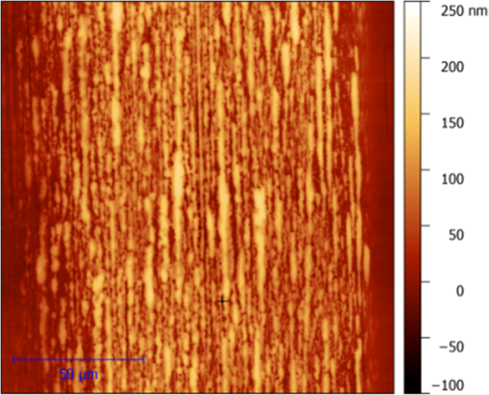
ZDDP tribofilms were formed by rubbing a steel ball on a steel disc immersed in lubricant in a minitraction machine (MTM) at a low entrainment speed [1]. The lubricant was a secondary ZDDP at 0.08 wt%. P concentration in a Group II oil containing a non-functionalised olefin copolymer VM. The blend had a viscosity of 7.53 mPa s at 100 °C. Such a base oil/polymer blend is typical of that found in modern gasoline engine oils. MTM test conditions were as follows: load = 31 N, entrainment speed = 0.05 m/s, slide-roll ratio = 50%, temperature = 100 °C, test duration 3 h. This resulted in the formation of ZDDP tribofilm with mean thickness ca 100 nm. An AFM topography image of the film on an MTM disc is shown in Fig. 1. It has a typical elongated pad structure, with pads separated by deep valleys. Prior to FIB, the MTM disc was cleaned in heptane in an ultrasonic bath for 15 min.
3 FIB/TEM Study of Non-Gold-Coated Tribofilm
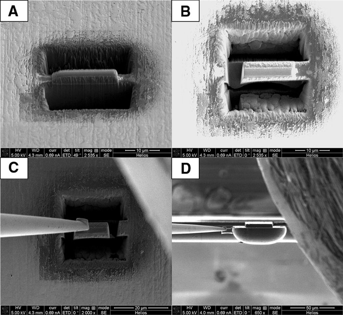
A Helios 600 NanoLab Focused Ion Beam (FIB) instrument was used to prepare ZDDP tribofilm specimens for study using Transmission Electron Microscopy (TEM). After the specimen was installed in the vacuum chamber, a protective Pt layer was applied using gallium-assisted ion beam deposition (acceleration voltage: 30 kV). This was followed by “bulk-out,” Fig. 2a, and “U-cut” milling, Fig. 2b, using Ga ions. Both processes are required to enable lift out of a prepared TEM specimen using a tungsten Omniprobe, Fig. 2c. The lifted specimen was then mounted on a copper grid, Fig. 2d, and this was followed by thinning and cleaning of the TEM specimen walls using Ga ions with reduced acceleration voltage. The parameters of each step are summarised in Table 1.
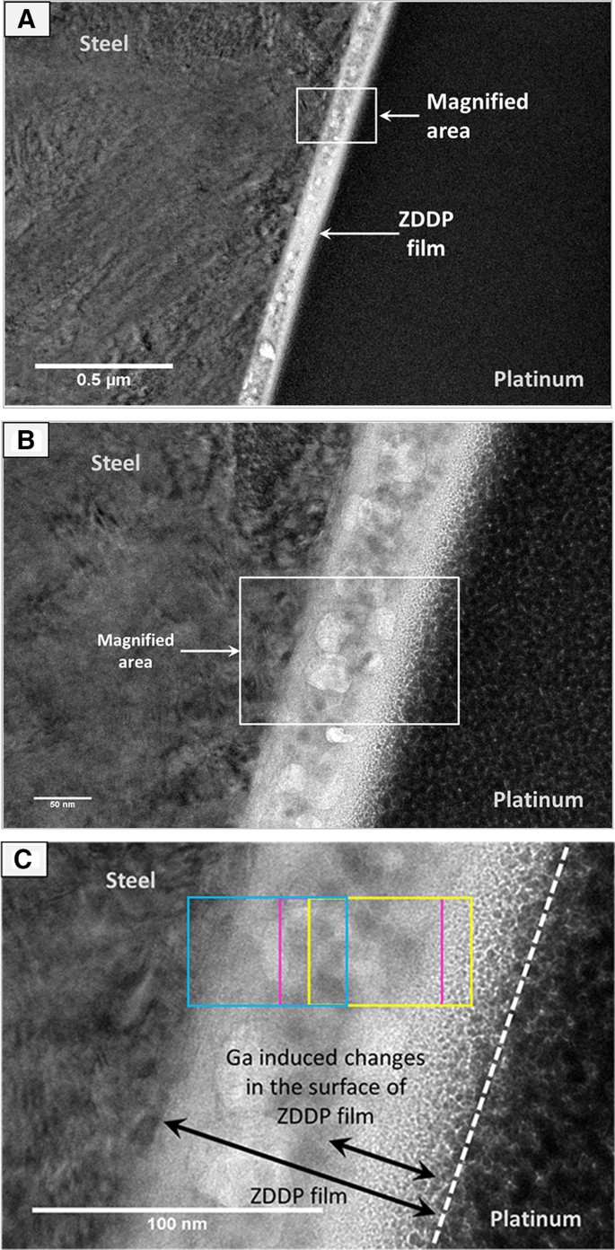
Figure 3a–c shows three different magnification TEM images of cross sections of ZDDP tribofilm. In these TEM images, dark areas represent regions of higher density. In Fig. 3a, it can be seen that the ZDDP film is around 100 nm thick, while in Fig. 3b, c it can be seen that the upper layer close to the Pt layer (ca. 30–40 nm) is different in appearance from the remaining part of tribofilm, with a relatively coarse light and dark network structure such that the interface between the upper layer of tribofilm and the deposited Pt, roughly marked with dashed white line on Fig. 3c, is hard to distinguish.
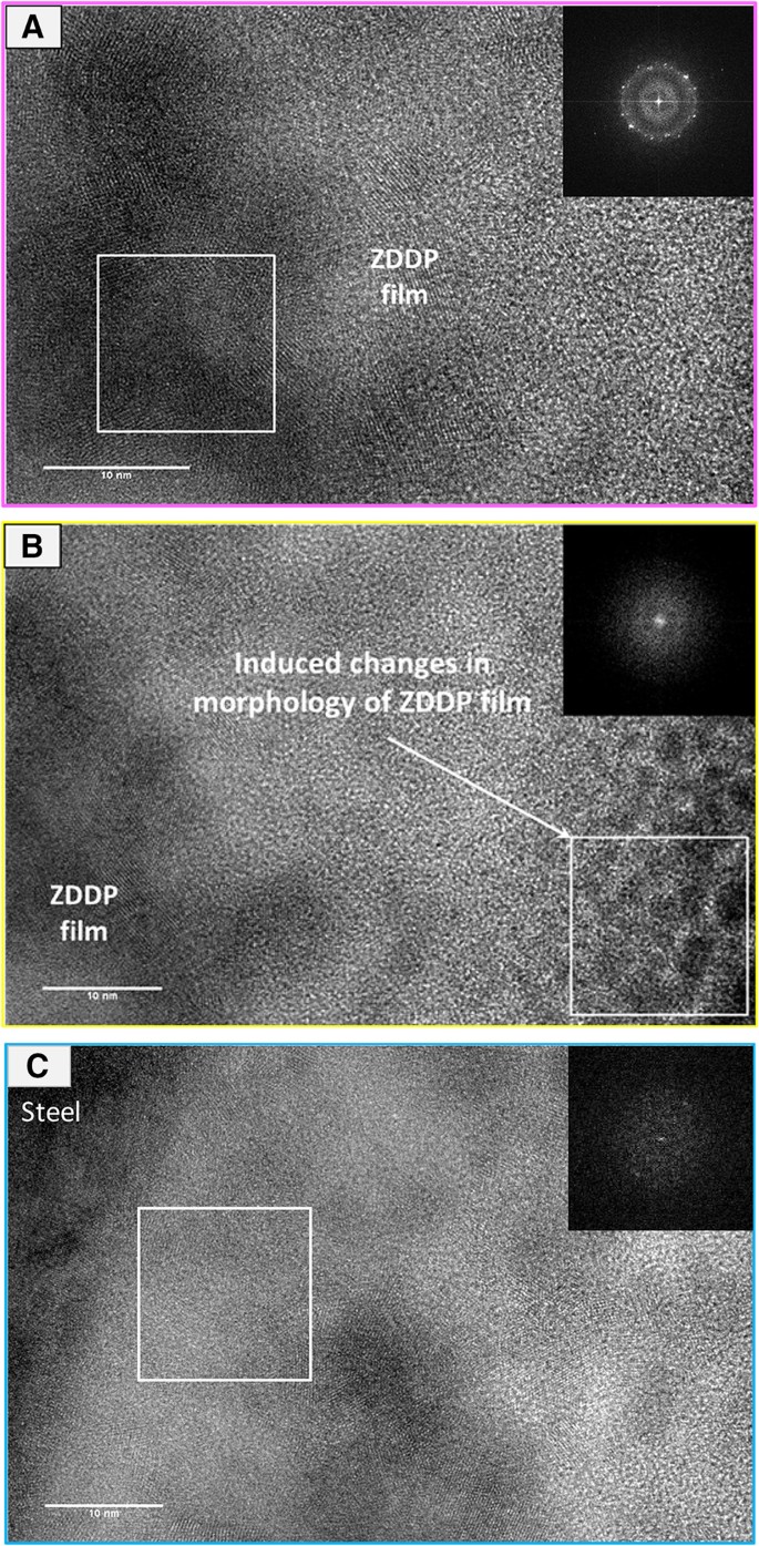
Deposition of Pt in the presence of Ga ions and Ga ion milling itself were possible causes of the difference in this upper region of the ZDDP tribofilm. The structure of the upper and central tribofilm regions were therefore compared using high-resolution images from the areas in Fig. 3c marked with pink, yellow and blue rectangles. When high magnification was applied in the middle region on tribofilm, Fig. 4a, ordered regions of apparent crystallinity can be seen. A diffraction pattern from the area marked on Fig. 4a with a white square is shown and confirms the presence of crystalline structure. In Fig. 4b, a diffraction pattern from the outer layer of tribofilm is shown. This region does not exhibit a crystalline structure diffraction pattern. Figure 4c shows the film very close to the steel substrate and suggests a mainly amorphous structure, though with some ordered domains.
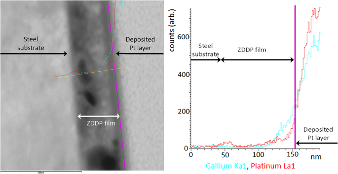
Scanning mode TEM (STEM) was applied in order to use energy-dispersive X-ray spectroscopy (EDX) to obtain elemental chemical analysis of TEM specimens. Figure 5 shows the distribution of platinum and gallium through the ZDDP film. For clarity, these data are also reproduced separate from the SEM image. Both the platinum and gallium penetrate into the upper third of the film and are thus likely to be responsible for the change in structure of this region.
4 FIB/TEM Study of Gold-Coated Tribofilm
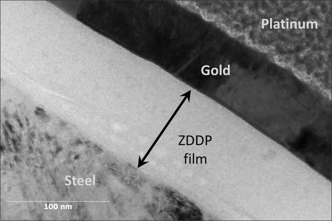
A Q150T Sputter Coater was used to deposit 60–70 nm of gold coating on a heptane-cleaned ZDDP tribofilm using a current of 30 mA prior to Pt deposition and FIB milling. The TEM in Fig. 6 shows that the tribofilm is slightly more than 100 nm thick. It is covered with ca. 60 nm of Au on top of which is the deposited layer of Pt. The interface between the tribofilm and Au layer is now very sharp, with none of the interpenetration seen when Pt was deposited directly on ZDDP. Indeed, the Pt/Au interface can be seen to be intercalated, suggesting that the high energy deposition of Pt disrupts the substrate on which it is deposited.
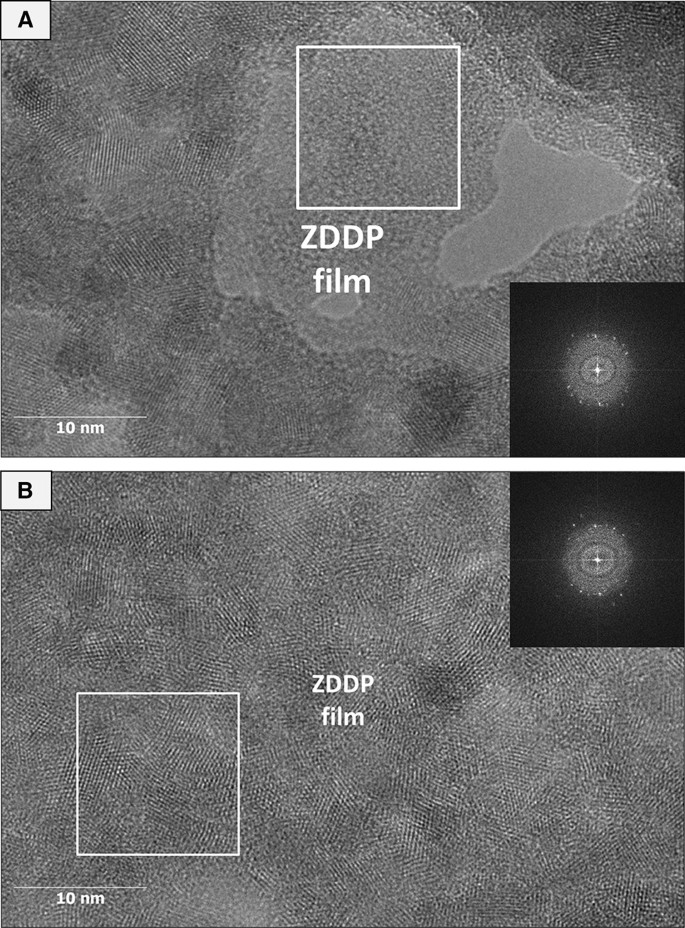
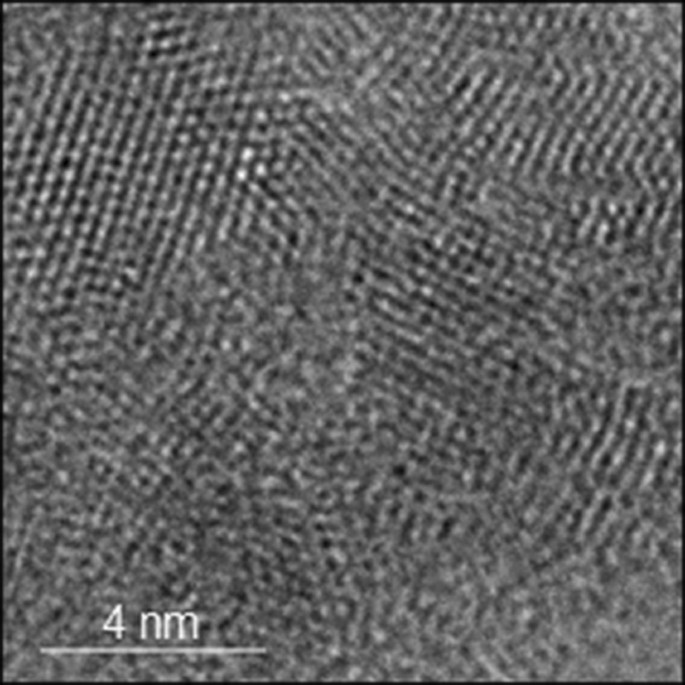
Figure 7a, b is at higher magnification. At this magnification, ordered regions can be seen over most of the film. Diffraction patterns obtained even close to the ZDDP tribofilm/Au interface (from the regions marked with white squares) show crystallinity. Figure 8 is a close-up image extracted from Fig. 7b to demonstrate more clearly the polycrystallinity; the film consists of close-packed crystalline domains of diameter ca 3–5 nm.
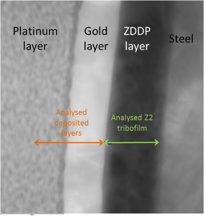
Figure 9 shows an STEM image of the cross section of ZDDP tribofilm that was coated with gold before the TEM specimen was prepared. When scanning mode is applied, the dark regions represent lower density regions. It should be noted that EDX analysis was more straightforward when performed on specimens that included a gold layer since the latter increased the yield of secondary electrons, thus increasing the contrast of the image.
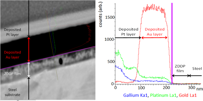
Figure 10 summarises the elemental chemical analysis across the deposited protective layers, along the line marked with an orange arrow on Fig. 9. The upper regions of Pt layer contain only Pt and Ga atoms, while spectra obtained 10 nm above the Au layer start to indicate the presence of Au atoms. The Pt/Au interphase contains predominantly Pt atoms, though the amount of Au atoms reaches nearly 20%. The middle of the Au layer is almost only Au atoms and this remains unchanged down to the Au/ZDDP film interface.
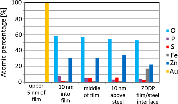
STEM-EDX analysis of the tribofilm was also carried out along the line marked with the green arrow in Fig. 9. This showed significant amounts of carbon, believed to originate from the cleaning solvent and this was excluded from the composition chart in Fig. 11, which shows the composition of the ZDDP tribofilm layer at various locations through the film. The region ca. 5 nm below the Au/ZDDP film interface contains only Au atoms and 10 nm below this interface the tribofilm contains predominantly O, Zn and P atoms. The middle regions of the tribofilm and those close to the steel surface contain slightly higher levels of S. The number of Fe atoms starts being significant only at the ZDDP film/steel interface.
5 Discussion
5.1 Damage to ZDDP Films Using FIB
This study has confirmed that care must be taken in the preparation of ZDDP tribofilm samples (and presumably other tribofilms) during FIB milling.
It is well known outside of tribology that high energy ion beam impact by both Ga and Pt ions induces changes in analysed surfaces, including amorphisation of metals and ceramics, and chemical changes to polymers [2,3,4,5,6,7]. Considerable efforts have been made to find ways to mitigate such damage and two main approaches have been developed. One is to deposit protective films at low energy prior to milling, applied either before insertion of the sample into the FIB facility or within the FIB chamber using electron deposition. Rubanov et al. showed that the high energy Ga ions used in FIB milling produced amorphisation of silicon but that this could be prevented by applying ca. 60–70 nm of a sputtered gold protective layer on the silicon surface [8]. Thinner gold films were less effective. Kempshell et al. explored various possible protective coatings and suggested application of ca. 30 nm thick Cr coating prior to Pt deposition [9]. An alternative approach is to use a lower energy ion beam for milling than the 30 keV normally applied [10, 11]. This reduces the thickness of the damaged region but at the expense of much longer milling times. Although the primary damage to surfaces in FIB results from the normal impact of the Ga ion beam, there is also some damage of, and deposition on, the sidewalls produced during milling [12]. However, this is relatively thin and can be removed during the thinning and polishing stage of the TEM specimen preparation using a low energy ion beam, as indicated in Table 1.
Despite all of this literature, the importance of using a quite thick, low deposition energy protective film when using FIB to study tribofilms has not previously been highlighted. Indeed it is often not possible to determine what, if any protective coating was used since this is rarely reported. In early work in tribology, no protective film is mentioned [13, 14] or a tungsten layer was applied [15], but more recently it has become common to use platinum or a thin layer of tungsten with a thicker overlay of platinum [16, 17]. Sometimes a gold film is used but either this is very thin and applied only to increase the yield of secondary electrons or to avoid sample charging [18, 19], or the reason for the film and its thickness are not reported [20]. One notable exception is recent work by Liu et al. [21] and Feng et al. [22] who deposited thick Cr and Cu layers on ZDDP tribofilms, both to protect the latter during FIB and also to provide a sacrificial layer that could be flattened to enable nanopillar compression measurement.
It should be noted that as well as protecting the tribofilm during milling, the application of a sputtered gold coating on a freshly prepared and cleaned ZDDP tribofilm has another advantage in that it serves to protect the surface from contamination during what may be a quite long interval before a scheduled FIB session.
5.2 Crystallinity of ZDDP Tribofilm
Most past studies of ZDDP tribofilms have considered ZDDP to form an amorphous, glassy or quenched liquid structure. Initial research applied EXAFS to wear particles and suggested that the presence of iron promoted amorphisation [23, 24] and amorphisation is often associated with the digestion of iron oxide particles [25]. However, amorphous films have also been observed using TEM when little if any iron was present [26]. More recently, it has been suggested that normally crystalline zinc orthophosphate can be amorphised at contact pressures greater than 7 GPa [27, 28].
The current study shows quite clearly using TEM that much of the ZDDP tribofilm present is polycrystalline. XANES analysis carried out on rubbed surfaces produced in parallel indicated that the film is primarily zinc orthophosphate, which is well known normally to have a crystalline structure [29]. This film appears to consist of randomly oriented crystalline domains of size ca 4 nm, as illustrated in Fig. 8. Based on EDX, the iron content of most of the film was negligible, so this was not available to induce amorphisation, if indeed it does so. It is noteworthy that the diffraction pattern of the film immediately adjacent to the steel substrate was much weaker than the middle of the film, as shown in Fig. 4c although some ordered domains are still visible. This may support partial amorphisation of the film due to Fe atoms.
As shown in Fig. 4b, the uppermost 30–50 nm of the non-gold-coated specimen was non-crystalline, strongly suggesting that the high energy impact of one or both of Pt and Ga ions induces amorphisation.
It is important to stress that this study has shown that one ZDDP tribofilm has a highly polycrystalline structure but this does not mean that all such films are crystalline. There appears to have been little recent research to explore the crystallinity of ZDDP tribofilms, but using FIB/TEM Ajayi et al. detected both crystalline and non-crystalline tribofilms formed from commercial and model lubricants [20]. They found the extent of crystallinity to depend on rubbing conditions, with less crystallinity at lower temperature, and they suggested that more amorphous tribofilms gave lower boundary friction than more crystalline ones. Unfortunately, the compositions of the lubricants tested were not provided, so it is not clear whether the tribofilms studied originated from antiwear or from detergent additives.
6 Conclusions
It has been found that the impact of high energy Pt and Ga ions during focussed ion beam milling (FIB) can cause significant morphological and structural changes to the upper 30–50 nm of ZDDP tribofilms. This can be mitigated by the low energy deposition of a quite thick gold layer prior to installation of the sample in the FIB facility. This problem, and its solution, have been quite widely reported in the non-tribology literature but have not been highlighted in the application of FIB to study tribological surfaces. It has also been found, using this gold pre-deposition method, that the bulk of the ZDDP tribofilm studied has a polycrystalline structure.
References
Fujita, H., Glovnea, R.P., Spikes, H.A.: The study of zinc dialkyldithiophosphate anti-wear film formation and removal process. Part I: experimental. Trib. Trans. 48, 558–566 (2005)
Mardinly, J., Susnitzky, D.W.: Transmission electron microscopy of semiconductor based products. MRS Online Proc. Libr. Arch. https://doi.org/10.1557/PROC-523-03 (1998)
Rubanov, S., Munroe, P.R.: Investigation of the structure of damage layers in TEM samples prepared using a focused ion beam. J. Mater. Sci. Lett. 20(13), 1181–1183 (2001)
Sugiyama, M., Sigesato, G.: A review of focused ion beam technology and its applications in transmission electron microscopy. J. Electron. Microsc. 53(5), 527–536 (2004)
Gianuzzi, L.A.: Introduction to FIB. Springer, New York (2005)
Mayer, J., Giannuzzi, L.A., Kamino, T., Michael, J.: TEM sample preparation and FIB-induced damage. MRS Bull. 32(5), 400–407 (2007)
Bassim, N.D., De Gregorio, B.T., Kilcoyne, A.L.D., Scott, K., Chou, T., Wirick, S., Cody, G., Stroud, R.M.: Minimizing damage during FIB sample preparation of soft materials. J. Microsc. 245(3), 288–301 (2012)
Hofmann, F., Tarleton, E., Harder, R.J., Phillips, N.W., Ma, P.W., Clark, J.N., Robinson, I.K., Abbey, B., Liu, W., Beck, C.E.: 3D lattice distortions and defect structures in ion-implanted nano-crystals. Sci. Rep. 7, 45993 (2017)
Rubanov, S., Munroe, P.R.: The effect of the gold sputter-coated films in minimising damage in FIB-produced TEM specimens. Mater. Lett. 57(15), 2238–2241 (2003)
Kempshall, B.W., Giannuzzi, L.A., Prenitzer, B.I., Stevie, F.A., Da, S.X.: Comparative evaluation of protective coatings and focused ion beam chemical vapor deposition processes. J. Vac. Sci. Technol. B 20(1), 286–290 (2002)
Kato, N.I., Kohno, Y., Saka, H.: Side-wall damage in a transmission electron microscopy specimen of crystalline Si prepared by focused ion beam etching. J. Vac. Sci. Technol. A 17(4), 1201–1204 (1999)
Rubanov, S., Munroe, P.R.: FIB-induced damage in silicon. J. Microsc. 214(3), 213–221 (2004)
Minfray, C., Martin, J.M., Esnouf, C., Le Mogne, T., Kersting, R., Hagenhoff, B.: A multi-technique approach of tribofilm characterisation. Thin Solid Films 447, 272–277 (2004)
Nehme, G., Mourhatch, R., Aswath, P.B.: Effect of contact load and lubricant volume on the properties of tribofilms formed under boundary lubrication in a fully formulated oil under extreme load conditions. Wear 268(9–10), 1129–1147 (2010)
Evans, R.D., More, K.L., Darragh, C.V., Nixon, H.P.: Transmission electron microscopy of boundary-lubricated bearing surfaces. Part II: Mineral oil lubricant with sulfur-and phosphorus-containing gear oil additives. Tribol. Trans. 48(3), 299–307 (2005)
Njiwa, P., Minfray, C., Le Mogne, T., Vacher, B., Martin, J.M., Matsui, S., Mishina, M.: Zinc dialkyl phosphate (ZP) as an anti-wear additive: comparison with ZDDP. Tribol. Lett. 44(1), 19–30 (2011)
Berkani, S., Dassenoy, F., Minfray, C., Belin, M., Vacher, B., Martin, J.M., Cardon, H., Montagnac, G., Reynard, B.: Model formation of ZDDP tribofilm from a mixture of zinc metaphosphate and goethite. Tribol. Int. 79, 197–203 (2014)
Li, Y.R., Pereira, G., Lachenwitzer, A., Kasrai, M., Norton, P.R.: Studies on ZDDP thermal film formation by XANES spectroscopy, atomic force microscopy, FIB/SEM and 31P NMR. Tribol. Lett. 29, 11–22 (2008)
Spadaro, F., Rossi, A., Ramakrishna, S.N., Lainé, E., Woodward, P., Spencer, N.D.: Understanding complex tribofilms by means of H3BO3–B2O3 model glasses. Langmuir 34(6), 2219–2234 (2018)
Ajayi, O.O., De La Lorenzo-Martin, M., Fenske, G.R.: Tribological synthesis method for producing low-friction surface film coating. U.S. Patent 9,476,007, (2016)
Liu, X., Tang, C.Y., Hao, R., Walsh, K., Zhou, C., Dillon, S.J.: Local chemo-mechanical insights into the efficacy of ZDDP additives from in situ single asperity growth and mechanical testing. Tribol. Int. 112, 103–107 (2017)
Feng, L., Hao, R., Gaemers, S., Warrens, C.P., Dillon, S.J.: Variation in zinc dialkyldithiophosphate yield strength measured by nanopillar compression. Tribol. Int. 123, 325–328 (2018)
Martin, J.M., Belin, M., Mansot, J.L., Dexpert, H.: Lagarde, P. Friction-induced amorphization with ZDDP—an EXAFS study. ASLE Trans. 29(4), 523–531 (1986)
Belin, M., Martin, J., Mansot, J.: Role of iron in the amorphization process in friction-induced phosphate glasses. J. Phys. Colloq. 48(C9), C9-1147–C9-1153 (1987)
Minfray, C., Le Mogne, T., Martin, J.M., Onodera, T., Nara, S., Takahashi, S., Tsuboi, H., Koyama, M., Endou, A., Takaba, H., Kubo, M.: Experimental and molecular dynamics simulations of tribochemical reactions with ZDDP: zinc phosphate–iron oxide reaction. Tribol. Trans. 51(5), 589–601 (2008)
Minfray, C., Martin, J.M., Esnouf, C., Le Mogne, T., Kersting, R., Hagenhoff, B.: A multi-technique approach of tribofilm characterisation. Thin Solid Film, 447, 272–277 (2004)
Shakhvorostov, D., Müser, M.H., Mosey, N.J., Munoz–Paniagua, D.J., Pereira, G., Song, Y., Kasrai, M., Norton, P.: On the pressure-induced loss of crystallinity in orthophosphates of zinc and calcium. J. Chem. Phys. 128(7), 074706 (2008)
Gauvin, M., Minfray, C., Belin, M., Aquilanti, G., Martin, J.M., Dassenoy, F.: Pressure-induced amorphization of zinc orthophosphate—insight in the zinc coordination by XAS. Tribol. Int. 67, 222–228 (2013)
Dawczyk, J.U.: The effect of organic friction modifiers on ZDDP tribofilm. PhD Thesis, Imperial College London (2018)
Acknowledgements
The authors thank Shell, who funded this research via the Shell University Technology Centre for Fuels and Lubricants at Imperial College London.
Author information
Authors and Affiliations
Corresponding author
Rights and permissions
Open Access This article is distributed under the terms of the Creative Commons Attribution 4.0 International License (http://creativecommons.org/licenses/by/4.0/), which permits unrestricted use, distribution, and reproduction in any medium, provided you give appropriate credit to the original author(s) and the source, provide a link to the Creative Commons license, and indicate if changes were made.
About this article
Cite this article
Dawczyk, J., Ware, E., Ardakani, M. et al. Use of FIB to Study ZDDP Tribofilms. Tribol Lett 66, 155 (2018). https://doi.org/10.1007/s11249-018-1114-y
Received:
Accepted:
Published:
DOI: https://doi.org/10.1007/s11249-018-1114-y


