Biotechnology applications are increasingly turning to CMOS integrated biosensor arrays for massive parallelism and increased throughput in biomolecular diagnostics [1, 2]. Yet many opportunities still remain to take advantage of the spatially-resolved nature of dense semiconductor platforms to open up new imaging dimensions [3, 4, 5] which complement traditional microscopy. To better understand the emergence of spatial organization in living systems, we require techniques that dynamically probe the spatial structure of assemblies of millions of cells or more. Optical microscopy is the dominant technique, but large field-of-view microscopes have an inherent tradeoff with resolving fine features. Confocal microscopes can image cellular-scale 3D structures, but their bright illumination can impart severe phototoxicity, and observing large areas can be prohibitively slow.
Here we present an integrated CMOS sensor array with 131,072 pixels, which is designed to electrochemically image and interface with bacterial biofilms. The architecture of the proposed multimodal CMOS sensor array is shown in Figure 1. Each pixel in the 512 x 256 array can be configured to measure impedance, pH, temperature, or electrochemical current, or perform bipolar voltage/current stimulation. In addition to its large active area and highly reconfigurable pixels, this is the first sensor in its class to support array-scale microscale electrical capacitance tomography through coordinated excitation and measurement from multiple pixels. Pixels are configured with row-wise and column-wise control signals, and each pixel has local SRAM to select between sensing and stimulation mode. Extensive circuit sharing is used to constrain each pixel to 10 μm x 10 μm.
Fig. 1.
Each of the 131,072 pixels can be configured for impedance, pH, temperature, amperometry, or bipolar stimulation and heating.
The integrated sensing array is fabricated in 180nm CMOS, occupying a total area of 25 mm2, including 13.1 mm2 active sensing area. The chip is wirebonded to a small printed circuit board, and the bondwires are encapsulated with epoxy. The top aluminum layer from the CMOS foundry is chemically etched from the pixels, leaving behind the titanium nitride (TiN) diffusion barrier as the sensing electrode surface [4]. Columns are directed into 8 parallel readout signal paths which include a pair of integrators followed by buffers to drive 8 external 500 kS/s 18bit ADCs. Correlated double sampling and chopping are applied to suppress offsets and 1/f noise. The sensor module is connected to a custom data acquisition board hosting an FPGA and USB 3.0 interface. System control and acquisition is managed through a Python environment. When active, the sensor consumes 58.8 mW, and full sensor frames take approximately 16 seconds to acquire.
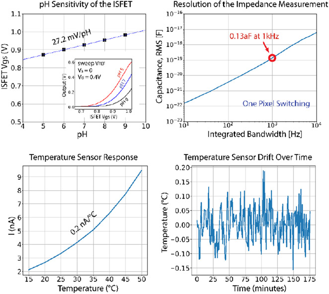
Impedance and capacitance sensing are established methods to detect cell adhesion and proliferation. In traditional non-integrated systems, impedance data is limited to a small number of scalar measurements, which limits the information available about spatial heterogeneity or morphology of the cell culture. Here, spatially resolved impedance measurements are assembled using a pair of non-overlapping clocks to rapidly charge and discharge each pixel’s electrode, while the transferred interfacial charge is integrated. The switched-capacitor circuits operate at radio frequency (up to 100MHz) which reduces Debye screening and allows observation of features farther from the surface [5]. The result is a high-resolution image of the dielectric properties of cells and other molecules near the surface of the sensor. Each pixel contains an N-channel ion sensitive field effect transistor (ISFET), which uses the same electrode as the impedance sensing mode. The measured pH sensitivity referred to the ISFET TiN gate is 27.2 mV/pH. Temperature fluctuations can have a significant impact on biofilm development, and the N channel ISFET can also be reconfigured as a temperature sensor, by diode-connecting its transistor and biasing it in subthreshold. Between 20°C and 40°C its sensitivity is approximately 0.2 nA/°C per pixel, and held at a constant temperature of 25°C for three hours the overall chip’s measured temperature fluctuation was ±0.17 °C. For interfacing with electrically excitable cell cultures, arbitrary patterns of bipolar voltage or current stimulation are supported by writing the stimulation state to each pixel’s SRAM. Current or voltage stimulation are achieved by configuring the pullup and pulldown transistors either as switches or as cascode current sources. This function can be used for electrically stimulating cell cultures as well as electroplating alternative electrode materials. In addition, closing both stimulation switches can generate resistive heating for spatially-programmable thermal stimulation.

We can apply this new sensor to produce state-of-the-art non-optical microscale maps of emergent structure within bacterial biofilms. Biofilms are communities of microbes that develop 2D and 3D morphology to coordinate their behaviors in response to environmental constraints and threats. There is great medical interest in combating biofilm infections, and biologists have made analogies between biofilm growth and embryonic development, highlighting the importance of biofilms as a transition to multicellularity [6]. Figure 2 shows a Bacillus subtilis biofilm (NCIB3610) on the CMOS chip, and an impedance image from the sensor. This strain expresses a red fluorescent protein (mScarlet), allowing simultaneous optical observation (Olympus MVX10 microscope). There are strong correlations between the fluorescence and impedance images, and in fact many secondary structures are more clearly resolved in the impedance data.
Fig. 2.
A Bacillus subtilis biofilm in contact with the sensor. Complex structure within the biofilm correlates well between the sensor’s impedance images and optical fluorescence imaging.
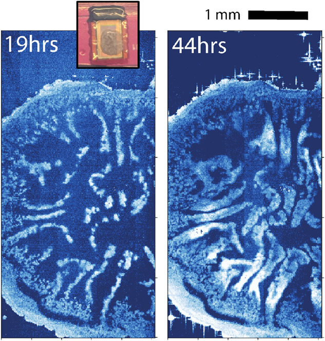
The new sensor can acquire temporally-resolved as well as spatially-resolved electrochemical images. In later stages of their development, biofilms can develop wrinkled 3D morphologies. In Figure 3, we show two impedance snapshots of microscale wrinkles emerging over time in a mutant strain of B. subtilis that overexpresses extracellular matrix (ΔsinR) [6]. High-impedance regions (white bands in Fig. 3) represent biofilm wrinkles that are in closer contact with the CMOS sensor, reducing the local dielectric constant. After 25 hours, the wrinkles have grown substantially.
Fig. 3.
Strains of B. subtilis which overexpress extracellular matrix polymers develop large wrinkles and complex morphology, which can be tracked over time with impedance imaging.
Biofilms often exist at 2D interfaces, but they have important 3D microstructure. In addition to producing 2D impedance images, the CMOS sensor incorporates depth sensitivity via computation of 3D permittivity distributions using electrical capacitance tomography. By rectifying and integrating the AC current from one pixel while switching a second pixel with opposite clock phases, the sensor can produce parasitic-insensitive measurements of the mutual capacitance CM between arbitrary pairs of pixels. The distance between two pixels affects the out-of-plane depth of the resulting AC electric field. Measurements from multiple overlapping pairs of pixels can then be computationally combined to produce an inverse estimate of the 3D permittivity distribution within a sample. The useful reconstruction depth extends tens of microns above the sensor, which is appropriate for imaging biofilm thickness profiles and permittivity maps. Figure 4 shows an experimental reconstruction of the dielectric permittivity of a 20 micron polystyrene bead on the sensor.
Fig. 4.
Electrical capacitance tomography can be used to estimate out-of-plane sample permittivity.
Using a new CMOS electrochemical imaging array, we have presented high-resolution, non-optical images which reveal biofilm structure at spatial resolution competitive with widefield fluorescence imaging. The sensor rapidly captures label-free, non-optical images over a large field of view. Expanded spatially-resolved sensing and stimulation modalities will enable insights into large-scale structural development within bacterial colonies, opening up new directions for the study of microbial communities.
Fig. 5.
The pH sensitivity of the ISFETs is 27.2 mV/pH. The impedance resolution is 0.13 attofarads (rms) for a 1 ms integration period, which would correspond to an acquisition time of 16 seconds per frame. At 25°C, the overall chip temperature measured variation less than ±0.2°C over three hours.
Fig. 6.
Comparison table.
References:
- [1].Rothberg JM et al. , Nature, 2011, DOI: 10.1038/nature10242 [DOI] [Google Scholar]
- [2].Huang X et al. , TBioCAS, 2015, DOI: 10.1109/TBME.2015.2419233. [DOI] [Google Scholar]
- [3].Park JS et al. , TBioCAS, 2018, DOI: 10.1109/TBCAS.2017.2759220. [DOI] [Google Scholar]
- [4].Hu K et al. , SSCL, 2021, DOI: 10.1109/LSSC.2021.3056515. [DOI] [Google Scholar]
- [5].Widdershoven F et al. , TBioCAS, 2018, DOI: 10.1109/TBCAS.2018.2861558. [DOI] [Google Scholar]
- [6].Vlamakis H et al. , Nature Reviews Microbiology, 2013, DOI: 10.1038/nrmicro2 [DOI] [Google Scholar]


