Thin Solid Films 520 (2012) 6455–6458
Contents lists available at SciVerse ScienceDirect
Thin Solid Films
journal homepage: www.elsevier.com/locate/tsf
Pulsed electron beam deposition of transparent conducting Al-doped ZnO films
Pham Hong Quang a,⁎, Ngo Dinh Sang b, Do Quang Ngoc a
a
b
Hanoi University of Science, Vietnam National University, Hanoi, 334 Nguyen Trai, Thanh Xuan, Hanoi, Viet Nam
National University of Civil Engineering, 55 Giai Phong Street, Hai Ba Trung, Hanoi, Viet Nam
a r t i c l e
i n f o
Article history:
Received 9 November 2011
Received in revised form 9 July 2012
Accepted 9 July 2012
Available online 16 July 2012
Keywords:
Zinc oxide
Doped II–VI semiconductors
Pulsed electron beam deposition
Thin films
Microstructure
a b s t r a c t
Good quality transparent conducting Al-doped ZnO films were deposited on quartz substrates from a high
purity target using pulsed electron deposition (PED). Two series of films were made, one deposited at
room temperature but at four pressures, viz., 0.7, 1.3, 2.0 and 2.7 Pa of oxygen and one deposited at 1.3 Pa
oxygen pressure but at the substrate temperature ranged from room temperature to 600 °C. In order to evaluate the effect of substrate temperature and oxygen pressure on the properties of obtained films, various
characterization techniques were employed including X-ray diffraction, stylus profiler, scanning electron microscope, optical spectrophotometer and electrical resistivity. For the first series films, the optimal oxygen
pressure of 1.3 Pa was found to bring about the appropriate energetic deposition atoms which results in
the best crystallinity. For the second series films, the lowest resistivity was obtained in the film grown at
400 °C. An attempt was made to reduce the resistivity by lowering the oxygen pressure to 0.5 Pa which
was the lower limit of working pressure of the PED system. The obtained results indicate that PED is a suitable
technique for growing transparent conducting ZnO films.
© 2012 Elsevier B.V. All rights reserved.
1. Introduction
Recently, much attention has been paid on zinc oxide which is a
highly transparent semiconductor in the visible region with a wide
band gap of ~3.37 eV at room temperature and a high excitonic binding
energy of ~60 meV [1]. When doped with group-III elements, such as Al,
Ga and In, its resistivity could be reduced to 2–4 × 10 −4 Ω.cm. With
these features, ZnO is a promising material for fabricating a variety of
devices such as transparent conducting electrode for flat panel displays
and solar cell, optoelectronic devices [2–7]. There are a wide variety of
methods for producing ZnO for fundamental studies or fabrication
of devices including RF sputtering [8], molecular beam epitaxy [9],
metal-organic chemical vapor deposition [10], vapor transport [11],
pulsed filtered cathodic arc deposition [12] and pulsed laser deposition (PLD) [13,14]. In particular, the pulsed laser deposition method
has been used for growth of transparent conducting ZnO films such
as Al, Ga and Er doped ZnO films [15–18]. However, limitations of this
technique include high cost of laser source, eye-safety requirements, as
well as issues related to scalability. More recently, pulsed electron deposition (PED) has been considered as an alternative deposition technique
for the formation of high quality ZnO thin films. In PED technique instead
of photons, energetic electrons are used to ablate the ceramic target.
Therefore, this method will work with materials that are transparent to
ultraviolet photons. Besides the advantage as in PLD that the stoichiometry of target materials is preserved in the film, PED is scalable, simple,
⁎ Corresponding author. Tel./fax: +84 438584438.
E-mail address: phquang2711@yahoo.com (P.H. Quang).
0040-6090/$ – see front matter © 2012 Elsevier B.V. All rights reserved.
doi:10.1016/j.tsf.2012.07.027
and low cost, making this technique become a suitable tool for growing
films of complex materials.
Growth of pure ZnO films by PED has been reported by H. L. Porter
et al. [19], M. Nistor et al. [20] and P. Zhan et al. [21]. In these works,
the films with high crystalline and optical quality have been obtained
and the effect of substrate temperature and oxygen pressure on the
crystallinity and surface morphology has been studied. In this paper,
we report the growth of transparent conducting Al doped ZnO film
by PED. Moreover, several issues concerning the optimal growth conditions in order to get good quality transparent conducting ZnO film
have been addressed in this paper.
2. Experiment
Al-doped ZnO (AZO) thin films were deposited on glass and quartz
substrates using PED technique. The pulsed electron gun used in our
experiments is a commercial source, PEBS-20 manufactured by
Neocera, Inc. It has the following technical specifications: discharge
voltage of 5–20 kV, beam energy of 0.2–0.8 J, pulse duration of
100 ns, maximum power density of 1.3 × 10 8 W/cm 2, beam cross
section of about 6 × 10 − 2 cm 2, and pulse frequency of 1–10 Hz. The
distance between target and substrate was 60 mm. In order to enhance the uniform erosion and reduce the “conic effect” on the surface of target, a target rastering feature was made by the movement
of the target stage at the X–Y plane about the central axis of the
stage. Start angle, end angle, and desired speed of rastering can be
selected by the user using computer. In all our experiments, the discharge voltage was maintained at 14 kV and the pulse frequency was
�6456
P.H. Quang et al. / Thin Solid Films 520 (2012) 6455–6458
maintained at 5 Hz. We chose the discharge voltage as 14 kV because,
according to M. Strikovski et al. [22], this is the optimal potential for
obtaining the maximum deposition rate. We made two series of films,
one deposited at room temperature but at four pressures, viz., 0.7, 1.3,
2.0 and 2.7 Pa of oxygen (named AZO-1), and one deposited at 1.3 Pa
oxygen pressure but at the substrate temperature ranged from room
temperature to 600 °C (named AZO-2). During deposition process, the
pressure was maintained by controlling the balance between the rate
of high vacuum pump and the flow of oxygen gas introduced into the
chamber. The target used is a high purity commercial 2 wt.% Al2O3
doped ZnO target of diameter 2 in. and thickness 3 mm. All samples
were deposited with 20,000 pulses.
The crystallinity of the films was characterized by X-ray diffraction
using Cu-α radiation (XRD, Bruker D5005) in a special configuration
where the incident angle was kept at 1.5°. Thickness was examined
by stylus profiler (VEECO-Dektak D150). Surface morphology was examined by a scanning electron microscopy (SEM, Jeol — JSM5410LV)
at a voltage of 15 keV. The optical properties were measured using
UV–vis spectrophotometer (UV — Shimadzu 2450) in the wavelength
range from 200 to 800 nm. The electrical resistivity was determined
by four probe technique at room temperature.
3. Results and discussion
3.1. Morphology, thickness and crystallinity
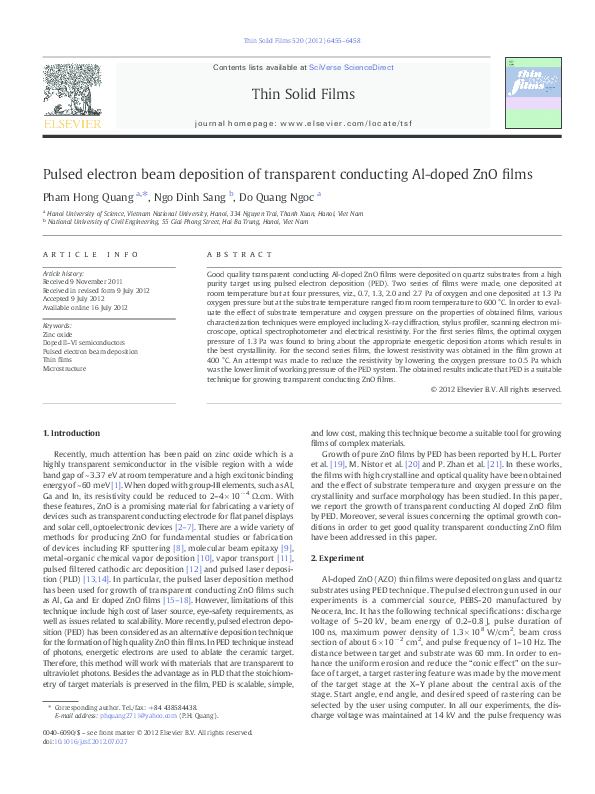
Fig. 1 shows three typical SEM images of the films grown at different
conditions. As seen in these pictures, particulates in the range from 50
to about 100 nm are present on the surface of the films, whatever the
condition of deposition. However, the density and the size of the particulates are smaller in the films deposited at a higher pressure. The origin
of these particulates is a matter of discussion. They can be directly emitted by the target during electron beam ablation, or they can be formed
in the gas phase, during the transport of species from the target to the
substrate. A. Yousif et al. observed some bright spots on the surface of
ZnO thin films deposited by PLD that were considered to be micro particles and drops which are produced by ZnO target due to the large energy density of laser [23]. M. Nistor et al. also observed this problem [20]
and suggested the possibility to reduce it by careful optimization of the
electron beam parameters in relation to the target materials. The electron beam parameters include the electron kinetic energy, power density and beam cross section. We agree with this suggestion because
we believe that the particulates are caused by high evaporation rate of
target materials due to the pulse feature of the electron source. In addition, we suggested that the presence of gas ambient can have a significant role in the elimination of this problem.
The thickness of the films depends strongly on the oxygen pressure. The thickness of the films in series AZO-1 are 270, 250, 230
and 220 nm for the films grown at room temperature and at 0.7,
1.3, 2.0 and 2.7 Pa oxygen pressure, respectively. The thickness of
the films in AZO-2 series is almost identical with the value of about
250 nm. The decrease of the thickness with oxygen pressure can be
easily explained by the interaction between incoming ions in plasma
flux and gas atoms, resulting in a decrease of current of ions arriving
at the substrate.
Fig. 2 shows the XRD patterns of the AZO-1 films. It is clear that
the films grown at lower oxygen pressure (i.e. 0.7 and 1.3 Pa) exhibit
a wurtzite structure with a high preference for the (002) orientation
whereas the films grown at higher oxygen pressure (i.e. 2.0 and
2.7 Pa) exhibit an amorphous structure. The highest intensity of
(002) peaks for the film grown at 1.3 Pa indicates that this pressure
is the most suitable. The degradation of the crystallinity at high oxygen pressure has also been observed by S. M. Park et al. in the growth
of AZO films by using PLD [15] and has been attributed to the excess
oxygen that might induce defects in the films which, in our opinion,
should be the planar type. At the substrate temperature of 320 °C, P.
Zhan et al. have obtained crystalline ZnO films grown by PED at any
oxygen pressure in the range from 1.1 Pa to 2.4 Pa but the authors
have also reported that the oxygen pressure of 1.6 Pa is the most favorable value for obtaining the best crystallinity [21]. In our case,
the effect of oxygen pressure seems to be stronger and more obvious
because the films were grown at room temperature, so that the influence of temperature has been eliminated. The fact that oxygen pressure
has an optimal value originates from the requirement of the average energy per deposited atom which should be about 10–20 eV. This energy
on one hand is strong enough to complete the disruption of the columnar morphology of the growing film but on the other hand do not damage the surface. It is well-known that in PED and PLD techniques, with
the presence of background gasses during ablation, the species arriving
at the substrate loses their average velocity as they undergo through
scattering, thermalization and deceleration [24].
Fig. 3 shows the XRD patterns of the films in AZO-2 series. First of all,
we can see that all films exhibit a wurtzite structure with a high preference for the c-axis orientation perpendicular to the substrate surface.
The crystallinity evaluated from the intensity and full width at halfmaximum of the (002) peak improves with increasing substrate temperature up to 400 °C. Further increasing the substrate temperature leads to
a slight degradation in crystallinity. The grain size estimated from
Scherrer equation is about 30 nm for the best film, i.e. the one deposited
at 400 °C. Hirata et al. [15], and P. Zhan et al. [20] have reported the similar effect of substrate temperature on the crystallinity of the ZnO films
grown by PLD and PED. P. Zhan et al. attributed the promotion of the
(002) peak to the increase of adatom mobility as increasing substrate
temperature. P. Zhan et al. also explained the degradation of (002)
peak at high temperature by structure zone model proposed by J. A.
Thormton [25] and recently extended by A. Anders [26]. According to
this model, the films deposited at high temperature have zone three
structures which contain much more randomly oriented grains formed
by secondary nucleation and recrystallization.
3.2. Electrical properties
The electrical resistivity of both AZO-1 and AZO-2 is presented in
Table 1. We can see that the resistivity of AZO-1 films is very high.
Fig. 1. Typical SEM images of the films grown at different conditions: (a) at 2.7 Pa and room temperature, (b) at 1.3 Pa and room temperature, and (c) at 1.3 Pa and 600 °C.
�6457
P.H. Quang et al. / Thin Solid Films 520 (2012) 6455–6458
Table 1
Electrical resistivity of the prepared samples.
Fig. 2. XRD patterns of AZO films deposited at room temperature and various oxygen
pressures.
However, it is still possible to realize that the resistivity is lower for
the films deposited at lower oxygen pressure. For AZO-2 films, the resistivity decreases dramatically with increasing the substrate temperature up to 400 °C, and then increases slightly again. Park et al. [14]
have observed a similar phenomenon on undoped ZnO films grown
by PLD and attributed the decrease of resistivity to the increase of
both carrier concentration and carrier mobility. The slight increase
in resistivity of the films grown at high temperature was explained
by the contamination of C from quartz substrate. Hirata et al. [15]
reported that resistivity of Ga-doped ZnO films deposited by PLD decreases with increasing deposited temperature up to 300 °C which is
their highest investigated temperature. Since the facts that there is a
close relation between the crystallinity and conductivity and our
films are ZnO doped with Al, we suggest that the enhancement in
conductivity is mainly due to the increase of number of Al atoms really activated in matrix oxide to produce extra electrons in the
band. The resistivity of 3.4 × 10 −2 Ω.cm obtained at the optimal temperature is still quite high for the requirement of transparent
conducting oxide films (TCO). Noting that the resistivity of AZO-1 decreases with decreasing the oxygen pressure, we made an additional
Oxygen pressure (Pa)
Substrate temperature (°C)
Electrical resistivity (Ω.cm)
0.7
1.3
2.0
2.7
1.3
1.3
1.3
25
25
25
25
150
400
600
3 × 10⁻¹
5 × 100
6 × 101
4 × 10²
5 × 10⁻¹
3.4 × 10⁻²
8 × 10⁻²
film at 400 °C and at an oxygen pressure of 0.5 Pa which was the
lower critical working pressure of our system. In PED technique, a
too-low gas pressure may cause a divergence of electron beams because of mutual charge repulsion while there is little space charge
shielding [24]. The resistivity of this film is 2.4 × 10 − 3 Ω.cm, that is
one order lower than that of the best film of AZO-2 series. We believe
that the improvement in conducting property of this film has both
contributions from the presence of oxygen vacancies and Al‐doped
atoms. However, this resistivity is still one order higher than that
obtained by A. Anders et al. [12] using pulsed filtered cathodic technique (about 5 × 10 − 4 Ω.cm) and by A. O. Dikovska [17] using PLD
technique (2.4 × 10 − 4 Ω.cm).
3.3. Optical properties
The optical transmittance of the films in both series AZO-1 and AZO-2
is very high (more than 80%) in the range of 350–900 nm. It is worth to
note that there is a relation between the crystallinity and the transmittance, e.g. the highest value of transmittance (~90%) has been obtained
for the film that has the best crystallinity. This transmittance is comparable to those obtained by other techniques [12,17] and meets the application requirement of transmittance exceeding 80%. The relation between
the crystallinity and the optical property can be seen more clearly from
the absorption spectra. The absorption spectra of AZO-1 and AZO-2
films are shown in Fig. 4a and b, respectively. The absorption spectra
of AZO-1 films have a tail in the transparent zone. All AZO-2 films have
a typical absorption spectrum of a direct band semiconductor with a
sharp absorption edge. The value of band gap about 3.2 eV can be determined by extrapolating the square of the absorption coefficient versus
the photon energy curve. This value is somewhat lower than the value
of 3.37 eV measured on pure ZnO materials [1].
4. Conclusion
Al-doped ZnO films have been grown by using Pulsed Electron Deposition technique. The properties of the films such as morphology,
thickness, crystallinity, electrical resistivity and transmittance were
found to depend strongly on the deposition conditions. In terms of
electrical conducting requirement, the best film was obtained at the
lowest oxygen pressure and at 400 °C. The transmittance of the best
films has met the application requirement of TCO films while the resistivity is still rather high. In order to reduce the electrical resistivity,
further studies are necessary and will be done in future. The obtained
results indicate that PED is a suitable technique for growing transparent conducting ZnO films.
Acknowledgments
Fig. 3. XRD patterns of AZO films deposited at various substrate temperatures and oxygen pressure of 1.3 Pa.
The authors would like to acknowledge the financial support by
the project NAFOSTED 103.02.59.09.
�6458
P.H. Quang et al. / Thin Solid Films 520 (2012) 6455–6458
References
[1]
[2]
[3]
[4]
[5]
[6]
[7]
[8]
[9]
[10]
[11]
[12]
[13]
[14]
[15]
[16]
[17]
[18]
[19]
[20]
[21]
[22]
[23]
[24]
[25]
[26]
Fig. 4. Absorption spectra of AZO films deposited (a) at room temperature and various
oxygen pressures and (b) at various substrate temperatures and oxygen pressure of
1.3 Pa.
D.G. Thomas, J. Phys. Chem. Solids 15 (1960) 86.
D.C. Look, Mater. Sci. Eng. B 80 (2001) 383.
K.L. Chopra, S. Major, D.K. Pandya, Thin Solid Films 102 (1983) 1.
M.W.J. Prins, K.O. Grosse Holz, G. Muller, J.F.M. Cillessen, J.B. Giesbers, R.P.
Weening, R.M. Wolf, Appl. Phys. Lett. 68 (1996) 3650.
V. Tadeev, G. Delabouglise, M. Labeau, Thin Solid Films 337 (1999) 163.
E. Comini, G. Faglia, G. Sberveglieri, Z.W. Pan, Z.L. Wang, Appl. Phys. Lett. 81
(2002) 1869.
J.Y. Kim, E.R. Kim, Y.K. Han, K.H. Nam, D.W. Ihm, Jpn J. Appl. Phys. 1 (41) (2002)
237.
B.P. Zhang, K. Walcatsuki, N.T. Binh, N. Usami, Y. Segawa, Thin Solid Films 449
(2004) 12.
Y. Chen, D.M. Bagnall, H.J. Koh, K.T. Park, K. Hiraga, Z.Q. Zhu, T. Yao, J. Appl. Phys.
84 (1998) 3912.
Y. Liu, C.R. Gorla, S. Liang, N. Emanetoglu, Y. Lu, H. Shen, M. Wraback, J. Electron.
Mater. 29 (2000) 69.
D.C. Look, D.C. Reynolds, J.R. Sizelove, R.L. Jones, C.W. Litton, G. Cantwell, W.C.
Harsch, Solid State Commun. 105 (1998) 399.
A. Anders, S.H.N. Lim, K.M. Yu, J. Andersson, J. Rosen, M. McFarland, J. Brown, Thin
Solid Films 518 (2010) 3313.
R.D. Vispute, V. Talyansky, Z. Trajanovic, S. Choopun, M. Downes, R.P. Sharma, T.
Venkatesan, M.C. Woods, R.T. Lareau, K.A. Jones, A.A. Iliadis, Appl. Phys. Lett. 70
(1997) 2735.
J.F. Muth, R.M. Kolbas, A.K. Sharma, S. Oktyabrsky, J. Narayan, J. Appl. Phys. 85
(1999) 7884.
S.M. Park, T. Ikegami, K. Ebihara, P.K. Shin, Appl. Surf. Sci. 253 (2006) 1522.
G.A. Hirata, J. McKitrick, J. Siqueiros, O.A. Lopez, T. Cheeks, O. Contreras, J.Y. Yi, J.
Vac. Sci. Technol. A 14 (3) (1996) 791.
O.G. Dikovska, P.A. Atanasov, I.G. Dimitrov, S.E. Imamova, T. Vasilev, J.
Optoelectron, Adv. Mater. 11 (10) (2009) 1517.
Z. Pan, S.H. Morgan, A. Ueda, R. Aga Jr., A. Steigerwald, A.B. Hmelo, R. Mu, J. Phys.
Condens. Matter 19 (2007) 266216.
H.L. Porter, C. Mion, A.L. Cai, X. Zhang, J.F. Muth, Mater. Sci. Eng. B 119 (2005) 210.
M. Nistor, N.B. Mandache, J. Perriere, J. Phys. D: Appl. Phys. 41 (2008) 165205.
P. Zhan, Z. Li, Z. Zhang, Mater. Trans. 52 (9) (2011) 1764.
M. Strikovski, K.S. Harshavardhan, Appl. Phys. Lett. 82 (2003) 853.
A. Yousif, A.J. Haider, Eng. Tech. J. 29 (1) (2011) 58.
M. D. Strikovski, J. Kim, and S. H. Kolagani, Spinger Handbook of Crystal Growth
Part E (2010), p. 1193.
J.A. Thornton, Rev. Mater. Sci. 7 (1977) 239.
A. Anders, Thin Solid Films 518 (2010) 4087.
�