Available online at www.sciencedirect.com
Optical Materials 30 (2007) 645–651
www.elsevier.com/locate/optmat
TiO2 thin films prepared by sol–gel method for
waveguiding applications: Correlation between
the structural and optical properties
R. Mechiakh
b
a,1
, F. Meriche b, R. Kremer b, R. Bensaha
a,1
, B. Boudine
a,1
, A. Boudrioua
b,*
a
Laboratoire de céramiques, Université Mentouri de Constantine, Route Ain El-Bey 25000 Constantine, Algeria
Laboratoire Matériaux Optique Photonique et Systèmes, CNRS UMR 7132, Université de Metz et Supélec, 2 Rue E. Belin, 57070 Metz, France
Received 29 May 2006; received in revised form 25 January 2007; accepted 20 February 2007
Available online 11 April 2007
Abstract
Thin films of transparent titanium oxide (TiO2) are prepared by the sol–gel dip-coating technique. Structural and optical properties of
TiO2 thin films are investigated for different annealing temperatures and different number of coatings. X-ray diffraction (XRD) and
Raman spectroscopy analysis show that the anatase crystalline phase appears beyond 350 �C for the four layers TiO2 film. At higher
temperatures and for thicker films, we observe in addition to anatase the formation of brookite and rutile phases. The grain size calculated from XRD patterns increases as the temperature of annealing and number of dipping increase, from 11.9 to 17.1 nm for anatase
and decreases as the number of dipping increases, from 24.2 to 10.2 nm for brookite. Film thickness, refractive index, and porosity are
found to vary with treatment temperature and the number of coating. The obtained films are transparent in the visible range and opaque
in the UV region. Waveguiding properties are studied using m-lines spectroscopy. The best results indicate that our films are monomodes
TE0 at 632.8 nm with optical losses of 2 dB cm�1.
� 2007 Elsevier B.V. All rights reserved.
Keywords: TiO2 thin films; Sol–gel; Planar waveguide; Anatase; Brookite
1. Introduction
Titanium dioxide (TiO2) thin films are extensively studied because of their interesting chemical, electrical and
optical properties (high bandgap, transparent in the visible
range, high refractive index, high dielectric constant, and
ability to be easily doped with active ions) which are considered for various optical applications such as high refractive index component of multilayer optical filter, gas
sensors, antireflective coating, photocatalysts, planar waveguides [1–3]. Moreover, in recent years, rare-earth (Er, Tb,
Eu) doped TiO2 planar optical waveguiding thin films have
*
Corresponding author. Tel.: +33 (0)3 87 37 85 47; fax: +33 (0)3 87 37
85 59.
E-mail address: boudriou@metz.supelec.fr (A. Boudrioua).
1
Tel./fax: +213 31 63 50 18.
0925-3467/$ - see front matter � 2007 Elsevier B.V. All rights reserved.
doi:10.1016/j.optmat.2007.02.047
attracted much attention due to their potential application
in integrated optics: integrated optical amplifiers, up-conversion micro-lasers, planar microcavities, flat panel display [4–6]. Mixed with Silica, sol–gel (SiO2–TiO2) thin
films are a good host matrix for semiconductor nanocrystallites (CdS, ZnS, PbS, CdTe) with suitable linear and
non-linear optical properties which can be exploited to
make all-optical switches, digital signal regenerators [7,8].
TiO2 films have been made by a variety of techniques.
Sol–gel method has emerged as one of the most promising
process as it is particularly efficient in producing thin,
transparent, homogenous, multi component oxide layers
of many compositions on various substrates at low cost
and it allows the choice of refractive index and thickness
of the layer by changing preparation conditions. Furthermore, this method offers the possibility to easily incorporate rare-earth ions as optically active centres and
�646
R. Mechiakh et al. / Optical Materials 30 (2007) 645–651
semiconductors nanocrystals into highly transparent glass
[4–8].
Crystalline TiO2 film exist in three phases: anatase
(tetragonal), rutile (tetragonal), and brookite (orthorhombic) [9,10]. Rutile being the most stable and the formation
of its phase depends on the starting material, deposition
method and temperature treatment. Numerous literature
reports on the fabrication of TiO2 thin films by sol–gel
dip coating technique using many types of titanium alkoxide as precursors. Nishide et al. [11] used HNO3 as a catalyst to prepare titania sols and TiO2 films in the sol–gel
process. As the treatment temperature increases, the transformation from anatase to rutile occurs and the refractive
index of the films increases linearly. Kim et al. [12] studied
the influence of the temperature on the optical and structural properties of TiO2 thin films, used HCl as a catalyst
to prepare titanium solutions and thin films of TiO2 in their
sol–gel process. Their thin films crystallise, starting from
400 �C, into anatase, and are transformed into anatase–
rutile starting from 1000 �C; the refractive index increases
with temperature while porosity decreases due to shrinkage
and densification of the films. These studies indicate that
the optical and structural properties of TiO2 films depend
on the process conditions and the materials used in this
process.
In this paper, we report the study of the structural and
optical properties of TiO2 thin films deposited on indium
tin oxide (ITO) coated glass by sol–gel dip coating technique as a function of the preparation conditions. Structural evolution with annealing temperature are
investigated by X-ray Diffraction (XRD) and confirmed
by Raman Spectroscopy measurements. Transmittance,
refractive index and porosity of the films are also studied.
Finally, the waveguiding properties of the obtained thin
films are investigated using m-lines spectroscopy.
The main objective of this work is to establish the best
synthesis conditions of TiO2 sol–gel films in order to obtain
high quality transparent thin film waveguides that could be
used as a host matrix for rare-earth and/or semiconductor
nanocrystals for fluorescence and non linear integrated
optical applications.
2. Experiments
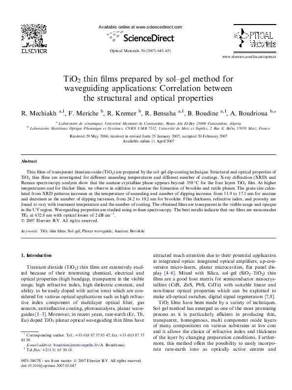
The TiO2 thin films were prepared by the sol–gel process, which is based on the hydrolysis of alkoxydes in alcoholic solutions in the presence of an acid catalyst. The
procedure of preparation includes the dissolution of one
mole of butanol (C4H9OH) as solvent and four moles of
acetic acid (C2H4O2), one mole of distilled water is added
as well as one mole of tetrabutyl–orthotitanate (C4H9O)4Ti
(Fig. 1); this solution is transparent, of yellowish color and
is ready for the deposit. The ITO glass (with refractive
index equal to 1.517 and thickness 20 Å) substrates carefully cleaned are dipped into the solution and are pulled
up at a constant rate of 6.25 cm/s. After each dipping, these
thin films are dried for 30 min at a distance of 40 cm from a
(C4H9O)4Ti
Tetrabutylorthotitanate
C4H9OH
C2H4O2
(H2O)
Mixing for 10 minutes
Mixing for 1 hour (Sol)
Gel
Substrates
Dipping + Withdraw
Drying (100˚C)
Xerogel
Heating
Oxide
Fig. 1. Sol–gel process of TiO2 thin film preparation.
500 W-light source (drying at 100 �C). The TiO2 thin films
were annealed in the temperature range of 300–450 �C with
increasing temperature rate of 5 �C min�1 for 2 h in furnace. To determine the transformation points, we have
analyzed the powder obtained from the xerogel by Differential Scanning Calorimetry (DSC) using a SETARAM
DSC–92 analyzer equipped with a processor and a measuring cell. The thermal cycle applied consists of heating from
room temperature to 520 �C, holding for 5 min at this temperature and finally cooling back to room temperature with
the same rate (5 �C/min). The variations of the lattice
parameter and the crystalline structure are determined by
an automated powder diffractometer (Siemens D5005)
using a copper anticathode at 40 kV, 20 mA over the 2h
range 10–70� (0.1�/s). The UV transmittance studies are
carried out using UV–Vis double–beam spectrophotometer
SHIMADZU (UV3101PC). Its useful range is between 190
and 3200 nm. The treatment of the spectra is performed
using the UVPC software. A surface profiler DEKTAK
3ST AUTO1 (VEECO) is used to determine film thicknesses. Raman spectra were recorded in a back scattering
configuration with a Jobbin Yvon micro Raman spectrometer coupled to a DX40 Olympus microscope. The samples
of the TiO2 thin films are excited with a 632.8 nm wavelength with an output of 20 mw.
Finally, the waveguiding properties (refractive index,
guided modes and optical losses) are investigated by dark
lines spectroscopy with a totally automated experimental
set-up. A right-angle rutile prism is used for coupling light
of a He–Ne laser with a wavelength k = 632.8 nm into the
waveguide. More details of the experimental arrangement
and theoretical analysis have been already discussed by
�647
R. Mechiakh et al. / Optical Materials 30 (2007) 645–651
205
(101)
.
4 layers
3. Results and discussion
Exo
80
Intensity (a.u.)
*
(b) 350ºC
*
(c) 400ºC
(a) xerogel
0
20
30
40
50
60
70
2θ (degree)
.
(110)
T from 400ºC
(101)
Intensity (a.u.)
.
120
(d) 450ºC
.
The thermal curve in Fig. 2 shows two singularities:
firstly, an endothermic peak spreading from 50 to 250 �C,
which corresponds to the evaporation of water, the thermal
decomposition of butanol as well as the carbonization or
the combustion of the acetic acid and certain elements
which constitute our alkoxyde and secondly, an exothermic
peak spreading from 290 to 410 �C, which corresponds to
the crystallization of titanium oxide.
This analysis shows that an annealing at a temperature
equal or higher than 400 �C would be largely sufficient to
form titanium oxide completely. Fig. 3a and b shows the
XRD patterns of the xerogel and the thin films of oxide
obtained after 4 dipping and various annealing temperatures at 350, 400 and 450 �C (a) and for various dipping
number (from 5 to 10) at annealing temperature of
400 �C (b). We observe that the crystallization occurs from
amorphous phase beyond 350 �C. These spectra, show a
peak corresponding to the (1 0 1) plane, which is attributed
to the presence of anatase regardless of the annealing temperature. At higher temperatures (400 and 450 �C) and for
a number of coating layers increasing from 4 to 7, we
observe in addition to anatase the formation of brookite
which crystallizes with the (1 2 1) plane parallel to the surface. These thin films deposited on ITO substrates annealed
at 350, 400 and 450 �C, are stoechiometric. We also observe
that the intensities corresponding to the lines characteristic
of anatase (1 0 1) and brookite (1 2 1) increase as the annealing temperature increases. This increase in the intensity of
the peaks leads us to deduce the amount of titanium oxide
as a function of the annealing temperature. Moreover,
Fig. 3b shows that for annealing temperature at 400 �C
and 10 layers, the crystalline structure changes from ana-
Heat Flow (W/g)
*
* (121)
3.1. Structural properties
100
: Anatase
:brookite
.
Tien and Ulrich [13]. The optical losses were determined
with a CCD camera by measuring the scattered light from
the surface film along the propagation direction.
.*
*
anatase
brookite
rutile
(121)
*
(d) 10 layers
(c) 7 layers
(a) 5 layers
(b) 6 layers
0
20
30
40
50
60
70
2θ (degree)
Fig. 3. X-ray diffraction pattern of TiO2 xerogel (a), and TiO2 thin films
on ITO glass obtained after 4 dippings and various annealings 350 �C (b),
400 �C (c) and 450 �C (d). X-ray diffraction pattern of TiO2 thin films
obtained after annealing at 400 �C for various number of dippings 5 (a), 6
(b), 7 (c), and 10 layers (d).
tase–brookite to rutile, which normally does not appear
below 800 �C as reported in the literature [14]. This phase
crystallizes with the (1 1 0) plane parallel to the surface.
The Raman spectra of Fig. 4a and b shows different
peaks related to the presence of titanium oxide in anatase
and brookite phases. In particular, Fig. 4b confirms the
presence of titanium oxide starting from the temperature
350 �C. These spectra exhibit bands at around 153 and
193 cm�1 which are assigned to TiO2 anatase [15].
60
3.2. Surface morphology and grain size
40
The crystallite size L of TiO2 thin films can be deduced
from XRD line broadening using the Scherrer equation
[16]:
20
0
Xerogel
0
100
200
300
400
500
600
T(ºC)
Fig. 2. The thermal curve of the xerogel recorded with 5 �C/min.
0:94 � k
1
L ¼ qffiffiffiffiffiffiffiffiffiffiffiffiffiffiffiffiffiffiffiffiffiffiffiffiffi
cos h
ðD2hkl � D2instr Þ
ð1Þ
�648
R. Mechiakh et al. / Optical Materials 30 (2007) 645–651
Table 1
Crystallite size L (nm) of the TiO2 thin films for different annealing
temperatures and different numbers of dipping
5000
T from 450ºC
.
7 layers
.
3000
*
2000
.
Intensity (a. u.)
4000
Phases
L (nm)
(hkl)
Xerogel
–
Amorphous
–
4 layers at 350 �C
4 layers at 400 �C
Anatase
Anatase
Brookite
11.9
12.3
24.2
(1 0 1)
(1 0 1)
(1 2 1)
4 layers at 450 �C
Anatase
Brookite
13.3
25
(1 0 1)
(1 2 1)
5 layers at 400 �C
Anatase
Brookite
15.7
12.4
(1 0 1)
(1 2 1)
6 layers at 400 �C
Anatase
Brookite
13.3
14.7
(1 0 1)
(1 2 1)
7 layers at 400 �C
Anatase
Brookite
Rutile
17.1
10.2
5.4
(1 0 1)
(1 2 1)
(1 1 0)
6 layers
5 layers
1000
Samples
: Anatase
: brookite
.
*
0
200
400
600
800
Raman Shift (cm-1)
10 layers at 400 �C
5000
400ºC
4 layers
100
(c)
Transmittance
.
2000
.
1000
80
350ºC
3000
.
Intensity (a. u.)
4000
: Anatase
(d)
(b)
(e)
60
(a)
40
(a) 4 layers at 400ºC
(b) 5 layers at 400ºC
(c) 6 layers at 400ºC
(d) 7 layers at 400ºC
(e) 10 layers at 400ºC
20
0
200
400
600
800
Raman Shift (cm-1)
0
400
Fig. 4. The Raman spectra of TiO2 thin films obtained after 4 dippings
and various annealings. The Raman spectra of a 450 �C heat-treated TiO2
thin films obtained for various numbers of dippings.
3.3. Optical properties
3.3.1. UV transmittance analysis
Fig. 5a and b shows the diffused scattering UV–Vis
transmittance spectra of TiO2 thin films for different
annealing temperatures and different number of dipping
in wavelength range 300–1000 nm. The transmission of
the titanium oxide thin films decreases with the increase
800
1000
Wavelength (nm)
100
80
Transmittance
k is the wavelength of X-ray beam (Cu Ka = 1.5406 Å),
Dhkl is the full width at half maximum (FWHM) of the
(hkl) diffraction peak, Dinstr is the FWHM corresponding
the instrumental limit, and h is the Bragg angle.
The computed values of the grain sizes are given in
Table 1. We have calculated the grain sizes of the thin films
for different temperatures of annealing and different numbers of dippings. We found that the crystallinity of the
obtained anatase particles increased from 11.9 to 17.1 nm
as the temperature of annealing and the number of dipping
increase, whereas the size of brookite crystallites decreases
with increasing dippings from 24.2 to 10.2 nm.
600
60
40
4 layers at 350ºC
4 layers at 400ºC
4 layers at 450ºC
20
0
400
600
800
1000
Wavelength (nm)
Fig. 5. UV–Vis transmittance spectra of the TiO2 thin film, for various
layers annealed at 400 �C. UV–Vis transmittance spectra of 4 layers TiO2
thin film, annealed at various temperatures.
in annealing temperature and in the number of dipping.
This can be linked with the formation stage of anatase
and with the increase in the grain size [14]. The bands
due to the interference color of the film appeared in the
wavelength range of 350–800 nm.
�649
R. Mechiakh et al. / Optical Materials 30 (2007) 645–651
�
1� 2
T max ðkÞ � T min ðkÞ
n ðkÞ þ n2S ðkÞ þ 2n0 nS
2 0
T max ðkÞ � T min ðkÞ
3.3.2. m-Lines measurements
m-Lines spectroscopy is a useful method to determine
the optogeometric parameters of waveguiding thin films,
such as thickness and refractive index [13]. It uses a prism
coupling method to launch the laser light into the optical
layer. In optical planar waveguides, light propagation can
occur within a thin layer of a transparent material when
its refractive index is higher than that of surrounding layers
and when the film has sufficient thickness to support at
least one guided mode. Besides, the waveguiding properties
of the film strongly depend on the microstructure of the
material: surface roughness, porosity, grain size and grain
boundaries which are connected to the fabrication process
parameters such as withdrawal rate, sol concentration,
treatment temperature and number of coating layers [20].
This study showed that almost of our TiO2 thin films
support only one guided TE polarized mode (transverse
Refractive Index
40
2.2
30
2.1
20
2.0
10
Refractive Index
Porosity
1.9
0
1.8
300
350
400
450
Temperature (ºC)
60
2.5
10 layers
2.4
50
2.3
40
2.2
2.1
30
2.0
Porosity (%)
Where nd is the refractive index of pore–free anatase
(nd = 2.52 [19]), and n is the refractive index of the porous
thin films.
For instance, Fig. 6 shows results of the calculation of
the refractive index (n) and porosity (p) of the thin films
of oxide obtained after 8 and 10 layers for different annealing temperatures. It is noted that the refractive index of the
thin films of titanium oxide increases with increasing treatment temperature and number of dipping (from 1.94 to
2.44 for 10 layers and from 1.82 to 2.37 for 8 layers). In
addition, porosity decreases from 48.5% to 7.7% for 10 layers and from 57.1% to 13.6% for 8 layers. This can be connected with the change in the crystalline structure (anatase,
anatase–brookite, and rutile), the increase in the size of the
grains and/or the density of the layers.
50
2.3
ð3Þ
where n0 is the refractive index of air, ns is the refractive index of substrate, Tmax is the maximum envelope, and Tmin
is the minimum envelope. The thickness of the films was
adjusted to provide the best fits to the measured spectra.
In this study, all the deposited films are assumed to be
homogeneous. The porosity of the thin films is calculated
using the following equation [18]:
�
�
n2 � 1
porosity ¼ 1 � 2
� 100ð%Þ
ð4Þ
nd � 1
8 layers
2.4
Refractive Index
S¼
60
2.5
Porosity (%)
The refractive index of the prepared TiO2 thin films was
calculated from the measured UV–Vis transmittance spectrum. The evaluation method used in this work is based on
the analysis of the UV–Vis transmittance spectrum of a
weakly absorbing film deposited on a non–absorbing substrate [17]. The refractive index n(k) over the spectral range
is calculated by using the envelopes that are fitted to the
measured extreme:
rffiffiffiffiffiffiffiffiffiffiffiffiffiffiffiffiffiffiffiffiffiffiffiffiffiffiffiffiffiffiffiffiffiffiffiffiffiffiffiffiffiffiffiffiffiffiffiffi
qffiffiffiffiffiffiffiffiffiffiffiffiffiffiffiffiffiffiffiffiffiffiffiffiffiffiffiffiffiffiffiffiffiffiffiffi
nðkÞ ¼ S þ ðS 2 � n20 ðkÞn2S ðkÞÞ
ð2Þ
20
1.9
Refractive Index
Porosity
1.8
300
350
400
10
450
Temperature (ºC)
Fig. 6. Refractive index and porosity of 8 layers TiO2 thin film, annealed
at various temperatures (from 300 to 450 �C). Refractive index and
porosity of 10 layers TiO2 thin film, annealed at various temperatures
(from 300 to 450 �C).
electric mode: TE0). For instance, Fig. 7 shows that the
best result is obtained in case of 9 layers annealed at
450 �C. This curve gives the variation of the reflected intensity versus the angle of incidence at the base of the prism
coupler. The intensity dip is synonymous of the excitation
of guided mode from which we can measure the effective
indices. By using this value and that of thickness measured
by the profilometer (the films thickness varies between 20
and 292.1 nm) in the guided mode dispersion equation,
we calculate the film refractive index nTE. The results are
reported in Table 2. Refractive index for 4–9 layers at
450 �C is found to be �2.064. However, one has to note
that we did not observe any TM modes. That is very likely
due to the coupling conditions which strongly depend on
the surface roughness of the films. Similar phenomenon
has been observed by Boudiombo et al. [21]. It was suggested that the undetected TM modes could be also due
to the crystallographic configuration of the films. Thus,
TM modes are difficult to excite than TE ones and therefore they might be considered as ‘‘missing’’ modes [22].
Besides, several reports indicated controversial results
concerning waveguiding properties of TiO2 thin films pre-
�650
R. Mechiakh et al. / Optical Materials 30 (2007) 645–651
Finally, propagation loss measurements at 632.8 nm
have been estimated from the guided mode spectra. Indeed,
optical losses are connected to the width of reflectivity dips.
Moreover, the scattered light from the guide surface has
been collected by using a CCD camera and analysed by
using specific software as reported in reference [24]. The
losses were found to be about of 2 dB cm�1. This result
emphasizes the interest of using our TiO2 thin films as a
waveguiding structure. Moreover, it is believed that a careful preparation process as well as an adequate post-deposition heat treatment is very likely to decrease the optical
losses to less than 1 dB cm�1.
1.450
Reflected Intensity (a. u.)
1.445
1.440
1.435
1.430
1.425
9 layers 450ºC 2h
Pol. TE
1.420
TE0
4. Conclusion
1.415
0
5
10
15
20
25
Angle of Incidence (º)
1.26
Reflected Intensity (a. u.)
1.24
1.22
TE0
1.20
4 layers 400ºC 2h
Pol. TE
1.18
1.16
0
5
10
15
20
25
Angle of Incidence (º)
Fig. 7. TE mode spectra obtained by measuring the reflected intensity vs
the angle of incidence for (a) 9 layers annealed at 450 �C and (b) 4 layers
annealed at 400 �C.
Table 2
Measured TE effective indexes, refractive indexes and thickness of the
TiO2 layers at 450 �C
Number
of layers
Annealing
temperature
(�C)
Film
thickness d
(±0.1 nm)
Effective
index
Nm ± 4 · 10�4
Refractive
index
no ± 4 · 10�4
4
6
7
9
450
450
450
450
177.3
215.0
277.0
292.1
1.8037
1.8573
1.9168
1.9207
2.0640
2.0653
2.0667
2.0600
layers
layers
layers
layers
pared by sol–gel method. For instance, Mugnier et al.
[23] reported TiO2 monomode waveguide (thickness
d � 80 nm) with 1 layer as well as multilayers (4 layers)
waveguide which were TE and TM multimode. This
emphasizes that waveguiding property of TiO2 thin films
strongly depend on sol elaboration, deposition conditions
and heat treatment.
In this work we reported the investigation of TiO2 thin
films prepared by sol–gel method for optical waveguiding
applications. X-ray diffraction and Raman spectroscopy
analysis show that the thin films obtained crystallize into
tetragonal titanium oxide anatase starting from the annealing at 350 �C. At higher temperatures (400–450 �C), we
also note the formation of the orthorhombic brookite
phase. Besides, for the sample with ten layers annealed at
400 �C, only tetragonal rutile is obtained. The calculation
of the grain size by Scherrer’s formula, gives us sizes varying from 5.4 to 25 nm for all structures. The analysis of the
UV–Vis transmission spectra shows that TiO2 thin films
are transparent in the visible range and opaque in the
UV region, irrespective of the treatment temperature and
the number of dipping. Finally, the investigation of waveguiding properties by using m-lines spectroscopy show
the excitation of one guided TE mode with optical losses
of 2 dB cm�1.
References
[1] D.P. Partlow, T.W. O’Keeffe, Appl. Opt. 29 (10) (1990) 1526.
[2] A. Brunik, H. Cztemastek, K. Zakrzewska, M. Jachimowski, Thin
Solid Films 199 (1) (1991) 45.
[3] L. Yang, S. Scott Saavedra, N.R. Armstrong, J. Hayes, Anal. Chem.
66 (8) (1994) 1254.
[4] A. Bahtat, M. Bouderbala, M. Bouazaoui, J. Mugnier, M. Druetta,
Thin Solid Films 323 (1998) 59.
[5] A. Conde-Gallardo, M. Garcia-Rocha, R. Palomino-Merino, M.P.
Velasquez-Quesada, I. Hernandez-Calderon, Appl. Surf. Sci. 212–213
(2003) 583.
[6] C. Mignotte, Appl. Surf. Sci. 226 (2004) 355.
[7] G.C. Righini, A. Verciani, S. Pelli, M. Guglielmi, A. Martucci, J.
Fick, G. Vitrant, Pure Appl. Opt. 5 (1996) 655.
[8] J. Fick, A. Martucci, M. Guglielmi, J. Schell, Fiber Integrated Opt. 19
(2000) 43.
[9] C.J. Brinker, G.W. Scherer, Sol–Gel Science: The Physics and
Chemistry of Sol–Gel Processing, Academic Press, New York, 1990.
[10] H. Bach, D. Krause, Thin Films on Glass: Schott Series on Glass and
Glass Ceramics, Springer-Verlag, Telas, 1997.
[11] T. Nishide, M. Sato, H. Hara, J. Mater. Sci. 35 (2000) 465.
[12] D.J. Kim, S.H. Hahn, S.H. Oh, E.J. Kim, Mater. Lett. 57 (2) (2002)
355.
[13] P.K. Tien, R. Ulrich, J. Opt. Soc. Am. 60 (10) (1970) 1325.
[14] S.H. Oh, D.J. Kim, S.H. Hahn, E.J. Kim, Mater. Lett. 57 (26–27)
(2003) 4151.
�R. Mechiakh et al. / Optical Materials 30 (2007) 645–651
[15] T. Ohsaka, S. Yamahoka, O. Shimomura, Solid State Commun. 30
(6) (1979) 345.
[16] B.D. Cullity, Elements of X-ray Diffraction, second ed., AddisonWesley, 1978.
[17] J.C. Manifacier, J. Gasiot, J.P. Fillard, J. Phys. 9 (11) (1976) 1002.
[18] B.E. Yoldas, P.W. Partlow, Thin Solid Films 129 (1–2) (1985) 1.
[19] W.D. Kingery, H.K. Bowen, D.R. Uhlmann, Introduction to
Ceramics, second ed., Wiley, New York, 1976.
[20] U. Selvaraj, A.V. Prasadarao, S. Komarneni, R. Roy, J. Am. Ceram.
Soc. 75 (5) (1992) 1167.
651
[21] J. Boudiombo, O. Baehr, A. Boudrioua, P. Thevenin, J.C. Loulergue,
A. Bath, Mater. Sci. Eng. B46 (1997) 96.
[22] P.J. Chandler, L. Zhang, J.M. Cabrera, P.D. Townsend, Appl. Phys.
Lett. 54 (14) (1989) 1287.
[23] J. Mugnier, M. Bahtat, L. Lou, F. Sommer, C. Bovier, R. Perrin,
Fabrication des guides d’onde optiques par la méthode sol–gel,
JNOG Paris, 1995.
[24] A. Roemer, E. Millon, B. Vincent, A. Boudrioua, O. Pons-Y-Moll,
R.M. Defourneau, W. Seiller, J. Appl. Phys. 95 (6) (2004) 3041.
�
 Faiza Meriche