+Model
SNB-10402; No. of Pages 7
ARTICLE IN PRESS
Available online at www.sciencedirect.com
Sensors and Actuators B xxx (2007) xxx–xxx
Microparticle photometry in a CMOS microsystem combining
magnetic actuation and in situ optical detection
U. Lehmann a,∗ , M. Sergio b , S. Pietrocola a , E. Dupont a ,
C. Niclass b , M.A.M. Gijs a , E. Charbon b
a
Institute of Microelectronics and Microsystems, Microsystems Laboratory 2, Ecole Polytechnique Fédérale de Lausanne (EPFL), Lausanne, Switzerland
b School of Computer and Communication Sciences, Ecole Polytechnique Fédérale de Lausanne (EPFL), Lausanne, Switzerland
Abstract
We present a hybrid CMOS-based microfluidic system that combines magnetic actuation of microparticles with in situ optical detection using
single photon avalanche diodes (SPADs). The decoupling of the principles used for actuation and sensing permits a high sensitivity with respect to
detection and particle handling. Single magnetic microparticles are transported within a glass micro-capillary positioned over an array of actuation
coils and are detected upon passage over a SPAD, where they block incident light and thus lower the photon count. Use of the photometry method
allows the determination of the particle size, which, in combination with a simultaneous measurement of the particle velocity, enables us to estimate
further particle properties, such as their magnetization. We present the successful manipulation, detection and evaluation of magnetic particles with
diameters ranging from 1 to 30 m.
© 2007 Elsevier B.V. All rights reserved.
Keywords: Microfluidics; CMOS; Microparticles; Optical detection; Magnetism; SPAD; Photometry
1. Introduction
Magnetic microparticles and their application in bioanalytical microfluidic systems have been steadily gaining
interest in recent years [1–3]. This progress is largely caused by
the advantage of generating comparatively large and long-range
magnetic forces that can be obtained independent of fluidic flow
pattern. Based on their application in macroscopic bench-top
procedures, the magnetic particles are often employed in
lab-on-a-chip systems to capture biomolecules or cells of
interest and transport them to a chosen point, e.g. for detection
or further processing [4–6]. In most cases, the actuation is
achieved by attracting the magnetic particles towards a wire or
a microcoil, where they serve as magnetic labels that can be
detected via magnetoresistive effects [7–9]. Further methods of
choice are the optical detection of fluorescently labeled particles
or the observation via a microscope [3,6]. The advantage of
optical detection in these cases is the absence of interaction
between actuation and detection, which permits an increased
sensitivity of the system. Both magnetoresistive and optical
∗
Corresponding author. Tel.: +41 2169 36759; fax: +41 2169 35950.
E-mail address: ulrike.lehmann@epfl.ch (U. Lehmann).
approaches have been shown to allow the detection of single
magnetic particles, even though differentiation between particle
sizes has not yet been demonstrated [3,10,11].
In this paper we present a CMOS-based system that combines guided magnetic actuation of single magnetic particles
with integrated optical detection. The magnetic manipulation
of the microparticles is achieved by modulating the topology
of a magnetic field over the chip surface via an array of
micro-coils [12,13]. This method allows a very precise control
of the microparticle position within a glass micro-capillary
and does not require external moving parts. The scale of the
system permits the manipulation of single magnetic particles of
different sizes (1–30 m). The use of single photon avalanche
diodes (SPADs), positioned in the centers of the actuation coils
ensures the optical detection with the necessary high sensitivity
[14]. We evaluate the optical signal based on transit photometry,
a method rather known from astronomy [15], but, as we show,
also applicable for the microworld.
2. Design and working principle
In order to achieve a high flexibility of the system, we chose
a hybrid approach, combining a CMOS chip with an exchangeable microfluidic system. The CMOS chip, comprising four
0925-4005/$ – see front matter © 2007 Elsevier B.V. All rights reserved.
doi:10.1016/j.snb.2007.10.021
Please cite this article in press as: U. Lehmann, et al., Microparticle photometry in a CMOS microsystem combining magnetic actuation and in
situ optical detection, Sens. Actuators B: Chem. (2007), doi:10.1016/j.snb.2007.10.021
�+Model
SNB-10402; No. of Pages 7
2
ARTICLE IN PRESS
U. Lehmann et al. / Sensors and Actuators B xxx (2007) xxx–xxx
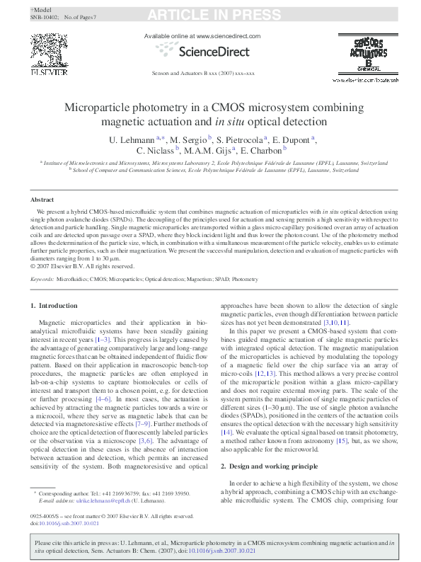
Fig. 1. Views of the CMOS chip: (a) explosion view showing the layers of the actuation system; (b) schematic sideview; (c) photograph of the system with insets of
the enlarged coil and SPAD.
metal layers, contains both the actuation and detection units.
The magnetic actuation is achieved via overlapping square
coils with each six windings of 35 m width, located in the
upper two metal layers of the chip. The SPADs, which serve as
detection units, are connected to the two bottom metal layers
and are positioned within a square opening of 20 m × 20 m
at the center of each coil. The coils are fabricated in 0.35 m
2P4M CMOS technology and the SPAD implementation is
based on a design presented recently by Niclass et al. [16].
Fig. 1 presents schematic views of the system in combination
with a photomicrograph of the chip including close-ups of a coil
and a center SPAD. A glass micro-capillary (Vitrocom), which
serves as model for future microfluidic systems, is placed on
top of the coils and contains the magnetic particles suspended in
an aqueous solution. The actuation of the magnetic particles is
achieved via a three-phase current scheme [13]. If one coil is set
to attractive mode, the adjacent coils are switched both to repulsive mode, thus increasing the magnetic field gradient, which
exerts a force on the particles into the desired direction. In order
to achieve attractive and repulsive modes, we alternate the direction of the coil currents. The absolute value of the dc current in
an active coil is 40 m, A which amounts to a power consumption
of 9 mW for each coil. Fig. 2 illustrates the topology of the
magnetic field during current switching and the subsequent
behavior of a cloud of magnetic particles. The particles are
additionally magnetized via a perpendicular homogeneous
Fig. 3. Schematics of a passively quenched SPAD: (a) 3D view of the CMOS
structure and (b) schematic diagram of the SPAD circuit.
magnetic field applied from outside the chip by means of an
electromagnet.
2.1. Optical detection
For the optical detection we profit from the advantageous
properties of a SPAD, which is a p–n junction reverse biased
above breakdown by an excess bias voltage Ve . This configuration, schematically shown in Fig. 3, causes the optical gain to
become virtually infinite, thus making single photon detection
possible. When a photon is absorbed in the multiplication
region, an avalanche is triggered. Thanks to a ballast resistance
placed in series to the p–n junction, the reverse bias temporarily
Fig. 2. Illustration of the particle transport: (a) analytical simulation of the perpendicular field ((+) attractive mode, (−) repulsive mode) and (b) photographs of
a particle transport sequence. The images of the fluorescent magnetic particles (∅ 5 m) are overlaid with a photograph of the CMOS chip. The duration of the
three-image sequence is 20 s.
Please cite this article in press as: U. Lehmann, et al., Microparticle photometry in a CMOS microsystem combining magnetic actuation and in
situ optical detection, Sens. Actuators B: Chem. (2007), doi:10.1016/j.snb.2007.10.021
�+Model
SNB-10402; No. of Pages 7
ARTICLE IN PRESS
3
U. Lehmann et al. / Sensors and Actuators B xxx (2007) xxx–xxx
via a computer interface, allowing simultaneous transport and
detection.
Fig. 4. Photon detection probability for different excess bias voltages Ve as a
function of the wavelength of impinging photons.
drops below breakdown and quenches the avalanche. The
combined duration of avalanche quenching and recharge time
determines the sensor’s dead time and in consequence the detection cycle of the SPAD. In this design, avalanche quenching is
achieved through a passive method. The measured dead time of
40 ns, resulting in a detection saturation count rate of 25 MHz,
is well below the time a particle requires for its transit between
coil centers. The voltage pulse obtained during a detection cycle
is regenerated and converted to a digital pulse by an inverter.
The probability that a digital pulse is generated upon impinging
photons, the photon detection probability (PDP), is plotted
in Fig. 4 as a function of excess bias voltage Ve and wavelength. The noise caused by a SPAD determines the minimum
detectable photon flux and is characterized by the frequency of
spurious pulses. These pulses are created by carriers that are
not photo-generated and their effect is known as the dark count
rate (DCR). It is caused by thermal or tunneling generated
carriers and is therefore a strong function of temperature and
excess bias voltage. In the present design, the DCR amounts to
750 Hz for an excess bias voltage of 3.3 V at room temperature.
The signals of the SPADs on the chip are recorded continually
2.1.1. Particle photometry
The optical detection of the actuated opaque spherical
magnetic particles is based on a photometry method [17]. The
SPAD is permanently illuminated using the light of a standard
reflective microscope (Zeiss Axioimager). When a particle is
passing over a coil center and the corresponding SPAD the
number of arriving photons and in consequence the intensity
of the light at the sensor is lowered, as schematically shown
in Fig. 5. The transit of microparticles can thus be described
as a micro-eclipse of the lightspot illuminating the SPAD. The
decrease (�I) in measured light intensity (I) depends on the
radius r of the passing particle (see schematic in Fig. 5c) and can
be derived from the geometric constellation of the system [17]:
� �2
Rp
r
�I
with Rp =
=
f + r and
I0
R∗
distSPAD
R∗ = (f + distSPAD ) tan(α)
(1)
Further parameters are the properties of the microscope
objective, such as its focal length f and numerical aperture
NA = n sin(α) with a refractive index of n = 1 for air, as well as
the distance between the particle and the SPAD (distSPAD ), with
distSPAD ≪ f. The influence of the capillary wall (n = 1.5) and the
liquid medium (n = 1.3) can be neglected since their thickness is
much smaller than the distance between the light source and the
particle. With all parameters known, the variation in the photon
count can be converted into the particle radius, following Eq. (1).
2.2. Particle velocity measurements
In addition to the determination of the particle size, the presence of multiple SPADs on the chip permits the determination
of further particle parameters such as the magnetization or the
magnetophoretic mobility [18]. Both can be determined via the
Fig. 5. Schematics of the optical detection principle based on photometry: (a) transition of the particle as seen from the sensor; (b) schematic graph of the light
intensity at the sensor; (c) model of the illumination during particle transit. The back-projected particle radius Rp is proportional to the amount of light blocked. Focal
length and numerical aperture are determined by the chosen objective.
Please cite this article in press as: U. Lehmann, et al., Microparticle photometry in a CMOS microsystem combining magnetic actuation and in
situ optical detection, Sens. Actuators B: Chem. (2007), doi:10.1016/j.snb.2007.10.021
�+Model
SNB-10402; No. of Pages 7
4
ARTICLE IN PRESS
U. Lehmann et al. / Sensors and Actuators B xxx (2007) xxx–xxx
measurement of the particle speed. Observing the SPADs of two
adjacent coils we can detect the moment of particle departure and
subsequent arrival at the next position. With the known distance
between the coil centers and the elapsed time, the particle velocity v can be estimated. Since the small dimensions of the system
lead to a Reynolds number smaller than 0.1, Stokes, Law can be
used to calculate the viscous drag acting on the moving particles.
Fd = 3πηDm v
(2)
Dm is the particle diameter, v the particle velocity and η is the
viscosity of the surrounding medium.
Analytical field simulations indicate a fairly constant
gradient of the magnetic flux density ▽B = 8 T/m, which results
in an equally constant magnetic force Fm on the particle of
volume Vm due to
Fm = Vm Hχm ∇B
(3)
with the magnetic field H and the particle’s magnetic
susceptibility χm .
Due to the magnetic design of the system, the magnetic
particles, which are statically magnetized via an external
magnetic field, are slightly lifted from the channel bottom
when the nearest coil changes into the repulsive mode. Thus
the particles float during the transport and are not hindered by
the friction with the capillary walls. This makes the magnetic
force and the viscous drag the governing forces in our system
and allows us to combine Eqs. (2) and (3) in order to obtain an
expression for the volume magnetization M of the particle:
3πηDm v
M = χm H =
Vm ∇B
Fig. 6. Photograph of a single 1 m magnetic microparticle partially occluding
a SPAD (50× objective).
3.1. Size detection via photometry
The experiments for the particle size detection were performed using a microscope objective with a long focal length
(Zeiss “Epiplan” 10×, NA = 0.2, f = 18.4 mm). The SPAD,
whose signal is recorded, is placed in the center of the objective’s lightspot. We count the pulses emitted by the SPAD circuit
using a LabView controlled computer interface (NI TB-2715,
National Instruments). The signals, measured during the passage
of microparticles of different sizes (1, 3 and 5 m), are plotted in
Fig. 7a. Since the maximum photon count varies between experiments, the signal was normalized to permit a better comparability of the measurements. A first comparison with the theoretical
model in Fig. 5b shows a strong resemblance between the curves,
which indicates the validity of the photometry approach.
3.2. Particle velocity measurements
(4)
The knowledge of the magnetization M enables us to
determine the particles’ volume magnetic moment m via the
known particle size and the amount of particles per gram given
by the supplier.
3. Experimental
We examined the magnetic and optical performance of
the system by manipulating magnetic particles of different
diameters (1, 3, 5, and 30 m) within a glass micro-capillary.
The walls of the glass capillary have a thickness of 25–100 m,
which lowers but also smoothens the magnetic field acting on
the particles with increasing thickness. The magnetic particles
follow the field gradient to the next corresponding coil center,
where they are optically detected by a SPAD. All experiments
were performed using a standard microscope with incident illumination (Zeiss Axio Imager.A1m with Hal 100 light-source)
set to an intensity that generates a photon count of 8 MHz at the
SPAD in the absence of magnetic particles. For the experiments
a highly diluted solution of magnetic particles (BangsLabs,
MicroMod, Spherotech) was used, which permits to manipulate
single particles. Fig. 6 shows a magnetic microparticle of 1 m
diameter positioned and held over a SPAD by the magnetic field.
In parallel with the particle size measurements we examined
the duration of particle displacement. The parallel observation
of two adjacent SPADs permits the detection of particle departure and arrival as visible in Fig. 7b. During the time interval �t
between the micro-eclipses over the neighboring SPADs, the
magnetic particle travels the distance of six windings, which
amounts to d = 210 m. The ratio of the traveled distance d
and the elapsed time �t is the average velocity of the magnetic
particle. Table 1 presents the average velocities measured for
different types of commercially available particles used in the
experiments.
4. Results and discussion
4.1. Particle size determination via photometry
An examination of Fig. 7a shows a dependence between the
decrease in photon count and the particle size, as expected from
Eq. (1). When comparing our measurements with the photometry model, we need to take the different wall thicknesses of
the capillaries used during experiments into account, and hence
the distance to the SPAD. The experiments for particles with
a diameter smaller than 15 m were performed in a capillary
with a wall thickness of 25 m, whereas larger particles
were manipulated in a capillary with 100 m thick walls.
Please cite this article in press as: U. Lehmann, et al., Microparticle photometry in a CMOS microsystem combining magnetic actuation and in
situ optical detection, Sens. Actuators B: Chem. (2007), doi:10.1016/j.snb.2007.10.021
�+Model
ARTICLE IN PRESS
SNB-10402; No. of Pages 7
5
U. Lehmann et al. / Sensors and Actuators B xxx (2007) xxx–xxx
Fig. 7. Signal of a SPAD during the passage of magnetic microparticles: (a) normalized photon count of a SPAD during the transit of single particles with 1, 3 and
5 m diameter and (b) photon count of two adjacent SPADs during particle transport for a particle of 5 m diameter showing the subsequent intensity drops.
Table 1
Comparison of the volume magnetization M for different types of magnetic particles obtained from velocity measurements
∅ (m)
Type
Vendor
Brand
Magnetite content (wt%)
v (m/s) (average)
M (A/m)
A
B
1
1.6
63.4
1.6
3600
42.5
2.9
2550
C
3
Superparamagnetic
BangsLabs
COMPEL
12.5
4.7
1180
Fig. 8 presents the theoretical and measured photon counts,
demonstrating a very good accordance between the photometry
model and experimental values. The increased variation for
smaller particles, that is visible in the graph, can be ascribed
to the size distribution of the particles, which is increasing for
smaller particles, and an uncertainty in the manipulation of
real particle singlets. Due to the optical observation system’s
constellation, the distinction between singlets and multiplets
of particles was not always possible for very small particles. A
comparison of the curves in Fig. 8 also shows that a decrease in
capillary sidewall thickness increases the system’s sensitivity
towards particle size. Thus a thinner capillary sidewall will
Fig. 8. Comparison of the measured and expected values for different particle
diameters and varying capillary wall thicknesses.
D
E
5
5
Ferrimagnetic
Spherotech
COMPEL
5.5
13
810
4.3
390
permit a better distinction between small particles. On the other
hand does the decrease in distance between the sensor and the
particle limit the maximum detectable size. Once the projected
particle radius Rp surpasses R* , the photon count will drop to
a minimum value common for all larger particles. Thus the
sidewall width of the capillary needs to be chosen according
to the range of particle sizes of interest in combination with
Eq. (1).
4.2. Particle velocity evaluation
Our measurements of the particle speed (Table 1) show
that the velocity, which is in the range of m/s, increases with
particle size and magnetite content. Based on the known particle
size and the parameters of the system, such as viscosity and
magnetic field gradient, we are able to convert the measured
velocity into the magnetization M according to Eq. (4). A
summary of the different magnetic particles is shown in Table 1.
A comparison with the magnetic content given by the particle
supplier, showed a dependence between the volume magnetization and the magnetite content, which is in agreement with
theory [19]. In Table 1 we can see, that a loss in magnetic force,
which scales by the order of three, can be offset by an increase
in magnetite content. The resulting larger magnetic moment
enables smaller particles to still overcome the viscous drag
force and move into a given direction. Our results additionally
indicate the influence of the magnetic particle properties.
Since ferromagnetic material is less easily magnetized than
the superparamagnetic particles, the volume magnetization is
smaller at the field strength present in the capillary.
Please cite this article in press as: U. Lehmann, et al., Microparticle photometry in a CMOS microsystem combining magnetic actuation and in
situ optical detection, Sens. Actuators B: Chem. (2007), doi:10.1016/j.snb.2007.10.021
�+Model
SNB-10402; No. of Pages 7
6
ARTICLE IN PRESS
U. Lehmann et al. / Sensors and Actuators B xxx (2007) xxx–xxx
The particle velocity also allows an estimation of the forces
obtained by the magnetic actuation. With a viscosity for water
of η = 1 mPa s we calculate forces on the particles in the upper
fN range, using Eq. (2).
5. Conclusion
Our experiments demonstrate the advantages and the
potential of the combination of magnetic actuation and optical
detection in one single CMOS chip. We are able to show the
possibility to actuate and detect single particles of 1–30 m
diameter, with a minimum distance to the sensor of 25 m,
using a modular system with an exchangeable microfluidic
component. We demonstrated that a decrease in the distance
between the sensor and the particle can increase the particle size
resolution, but limits the range of detection. The simultaneous
and automated detection of velocity and size of single particles
enables a wide range of particle characterizations and offers
many applications in bio-analytical systems [20]. Since the
principles of actuation and detection are not coupled, we can
envisage using the particles as mobile substrates to transport
biomaterials of interest, e.g. cells, and to perform on-chip analysis without interference between actuation and detection. With
magnetic particles enclosed within or attached to a single cell,
the latter can be transported and studied automatically within
the system. The size can be obtained via the micro-eclipse
measurements, while the determination of the velocity permits
calculating the content of bound or incorporated magnetic material in the cell or its surface, linked to chosen cells properties
[21].
In conclusion we can state that the combination of magnetic
actuation and integrated optical detection represents a promising
approach to miniaturized systems for on-chip bio-analysis.
Acknowledgements
The authors are grateful to Martin Lanz and Giovanni
Nicoletti for their technical support. The research was partially
supported by a grant of the Swiss National Science Foundation
(Grant 200020-107372) and the Competence Centre for
Materials Science and Technology (CCMX).
References
[1] M.A.M. Gijs, Magnetic bead handling on-chip: new opportunities for analytical applications, Microfluidics Nanofluidics 1 (1) (2004) 22–40.
[2] T. Deng, G.M. Whitesides, M. Radhakrishnan, Manipulation of magnetic
microbeads in suspension using micromagnetic systems fabricated with
soft lithography, Appl. Phys. Lett. 78 (12) (2001) 1775–1777.
[3] R. Wirix-Speetjens, W. Fyen, K.D. Xu, J. De Boeck, G. Borghs, A force
study of on-chip magnetic particle transport based on tapered conductors,
IEEE Trans. Magn. 41 (10) (2005) 4128–4133.
[4] U. Lehmann, C. Vandevyver, V.K. Parashar, M.A.M. Gijs, Droplet-based
DNA purification in a magnetic lab-on-a-chip, Angew. Chem. Int. Edit. 45
(19) (2006) 3062–3067.
[5] J.W. Choi, C.H. Ahn, S. Bhansali, H.T. Henderson, A new magnetic
bead-based, filterless bio-separator with planar electromagnet surfaces for
integrated bio-detection systems, Sens. Actuator B 68 (2000) 34–39.
[6] K. Smistrup, B.G. Kjeldsen, J.L. Reimers, M. Dufva, J. Petersen, M.F.
Hansen, On-chip magnetic bead microarray using hydrodynamic focusing
in a passive magnetic separator, Lab Chip 5 (11) (2005) 1315–1319.
[7] D.L. Graham, H.A. Ferreira, N. Feliciano, P.P. Freitas, L.A. Clarke, M.D.
Amaral, Magnetic field-assisted DNA hybridisation and simultaneous
detection using micron-sized spin-valve sensors and magnetic nanoparticles, Sens. Actuator B: Chem. 107 (2) (2005) 936–944.
[8] J.C. Rife, M.M. Miller, Design and performance of GMR sensors for the
detection of magnetic microbeads in biosensors, Sens. Actuator A 107
(2003) 209–218.
[9] H.A. Ferreira, N. Feliciano, D.L. Graham, P.P. Freitas, Effect of spin-valve
sensor magnetostatic fields on nanobead detection for biochip applications,
J. Appl. Phys. 97 (10) (2005).
[10] R. Wirix-Speetjens, W. Fyen, J. De Boeck, G. Borghs, Single magnetic
particle detection: experimental verification of simulated behavior, J. Appl.
Phys. 99 (10) (2006).
[11] H. Lee, A.M. Purdon, R.M. Westervelt, Micromanipulation of biological systems with microelectromagnets, IEEE Trans. Magn. 40 (4) (2004)
2991–2993.
[12] H. Lee, Y. Liu, D. Ham, R.M. Werstervelt, Integrated cell manipulation
system—CMOS/microfluidic hybrid, Lab Chip 7 (2007) 331–337.
[13] A. Rida, V. Fernandez, M.A.M. Gijs, Long-range transport of magnetic
microbeads using simple planar coils placed in a uniform magnetostatic
field, Appl. Phys. Lett. 83 (12) (2003) 2396.
[14] A. Rochas, M. Gani, B. Furrer, P.A. Besse, R.S. Popovic, G. Ribordy, N.
Gisin, Single photon detector fabricated in a complementary metal-oxidesemiconductor high-voltage technology, Rev. Sci. Instrum. 74 (7) (2003)
3263–3270.
[15] Z. Sandor, Estimations of orbital parameters of exoplanets from transit
photometry by using dynamical constraints, Celes. Mech. Dyn. Astron. 95
(1–4) (2006) 273–285.
[16] C. Niclass, M. Sergio, E. Charbon, A single photon avalanche diode array
fabricated in 0.35-m CMOS and based on an event-driven readout for
TCSPC experiments, in: Proceedings of the SPIE on Advanced Photon
Counting Techniques, vol. 6372, 2006, p. 63720S.
[17] P. Sartoretti, J. Schneider, On the detection of satellites of extrasolar planets
with the method of transits, Astron. Astrophys. Suppl. Ser. 134 (3) (1999)
553–560.
[18] K.E. McCloskey, J.J. Chalmers, Magnetic cell separation: characterization
of magnetophoretic mobility, Anal. Chem. 75 (2003) 6868–6874.
[19] L.C. Costa, M. Valente, M.A. Sa, F. Henry, Electrical and magnetic properties of polystyrene doped with iron nanoparticles, Polym. Bull. 57 (6)
(2006) 881–887.
[20] H.G. Chun, T.D. Chung, H.C. Kim, Cytometry and velocimetry on a
microfluidic chip using polyelectrolytic salt bridges, Anal. Chem. 77 (8)
(2005) 2490–2495.
[21] J.H. Clement, M. Schwalbe, N. Buske, K. Wagner, M. Schnabelrauch, P.
Gornert, K.O. Kliche, K. Pachmann, W. Weitschies, K. Hoffken, Differential interaction of magnetic nanoparticles with tumor cells and peripheral
blood cells, J. Cancer Res. Clin. Oncol. 132 (5) (2006) 287–292.
Biographies
Ulrike Lehmann was born in Rostock, Germany in 1978. She obtained her
Dipl-Ing. degree in electrical engineering, with a specialization on MEMS, in
2003, at the Chemnitz Technical University, Chemnitz, Germany. She currently
is a PhD student at the Ecole Polytechnique Fédérale de Lausanne (EPFL) in
the Laboratory for Microsystems, where she is working on the manipulation of
magnetic microparticles in liquid phases for application in biomedical systems.
Maximilian Sergio received the Dr. Eng. degree in microelectronics at the University of Bologna, Italy, in 1998. Since 2000, he has been working as full-time
consultant for the Central R&D Division of ST Microelectronics in Agrate Brianza (Milan, Italy) studying the utilization of STM CMOS technologies and
CAD platforms for the development and physical implementation of innovative
digital and mixed signals projects in particular in the field of smart sensors. In
2003, he received the PhD degree from the University of Bologna with the thesis
“Design of CMOS only smart pressure sensors”. From 2002 to 2004 he joined
Please cite this article in press as: U. Lehmann, et al., Microparticle photometry in a CMOS microsystem combining magnetic actuation and in
situ optical detection, Sens. Actuators B: Chem. (2007), doi:10.1016/j.snb.2007.10.021
�+Model
SNB-10402; No. of Pages 7
ARTICLE IN PRESS
U. Lehmann et al. / Sensors and Actuators B xxx (2007) xxx–xxx
the “Advanced Research Center on Electronic Systems E. De Castro (ARCES)”,
Bologna, Italy. The focus of his activity was on design of smart sensor using
standard CMOS technology. From 2005 to 2006 he was with the AQUA group at
EPFL where he worked on high-performance imaging and quantum integrated
circuits. Since 2007 he joined the Silicon Biosystems where he is the responsible
for analog and mixed-signal design of integrated sensors and actuators for living
cell manipulation.
Stefano Pietrocola was born in Torino, Italy, in 1982. He received the BS degree
in engineering mathematics from Politecnico di Torino in 2005, and the MS
degree in micro and nanotechnologies for integrated systems in collaboration
with the Politecnico di Torino, the INP de Grenoble and the EPFL, in September
2006. He is currently working at a spin-off of the University of Turin, Nanovector,
on the manipulation of nanoparticles for drug delivery systems.
Emile Dupont was born in Aosta, Italy, in 1982. He received his Bachelor degree
in information engineering from Politecnico di Torino in 2004 and his Master
degree in 2006 in the joint program held by Politecnico di Torino, INP Grenoble
and EPF Lausanne in micro and nanotechnologies with a master thesis titled
“From Macro to Micro Computational Fluid Dynamics: CFD Simulations at
CERN”. He is currently pursuing his PhD at EPFL in the Microsystems’ Group
leaded by Prof. Gijs, working on the manipulation of paramagnetic beads for
Bio-MEMS applications.
Cristiano Niclass received the MSc degree in microtechnology with emphasis
in applied photonics from EPFL in 2003. In May 2003, he joined the Quantum
Architecture Group (AQUA), where he is working toward the PhD degree. His
interests include high-speed and low-noise digital and mixed-mode applicationspecific integrated circuits with emphasis on high-performance imaging. He
is currently in charge of the design, implementation, and evaluation of fully
integrated two- and three-dimensional CMOS image sensors based on single
photon avalanche diodes. He is also involved in the design of time discrimination
devices with picosecond resolution implemented in conventional technologies.
Mr. Niclass is a member of the Institute of Electrical and Electronics Engineers
(IEEE).
7
Martin A.M. Gijs received his degree in physics in 1981 from the Katholieke
Universiteit Leuven, Belgium, and his PhD degree in physics at the same university in 1986. He joined the Philips Research Laboratories in Eindhoven,
The Netherlands, in 1987. Subsequently, he has worked there on microand nano-fabrication processes of high critical temperature superconducting
Josephson and tunnel junctions, the micro-fabrication of microstructures in
magnetic multilayers showing the giant magnetoresistance effect, the design
and realisation of miniaturised motors for hard disk applications and the
design and realisation of planar transformers for miniaturised power applications. He joined the Swiss Federal Institute of Technology Lausanne (Ecole
Polytechnique Fédérale de Lausanne) in 1997. He presently is a professor
in the Institute of Micro-electronics and Microsystems, where he is responsible for the Microsystems Technology Group. His main interests are in
developing technologies for novel magnetic devices, new microfabrication
technologies for microsystems fabrication in general and the development and use of microsystems technologies for biomedical applications in
particular.
Edoardo Charbon received the Diploma from ETH-Zürich, the MS from
UCSD, and the PhD from UC-Berkeley, all in EECS, in 1988, 1991, and 1995,
respectively. From 1995 to 2000, he was with Cadence Design Systems, where
he was the architect of the company’s initiative for intellectual property protection. In 2000, he joined Canesta Inc. as its Chief Architect, leading the
development of wireless 3D CMOS image sensors. Since November 2002,
he has been a member of the Faculty of EPFL, where he has founded the
Quantum Architecture Group (AQUA), a research group devoted to the field
of high-accuracy imaging and ultra low-power wireless embedded systems.
He has consulted for numerous organizations, including Texas Instruments,
Hewlett-Packard, Cadence, and the Carlyle Group. He has authored or coauthored over 90 articles in technical journals and conference proceedings and
two books, and he holds nine patents. His research interests include 3D microimaging, bio-imaging, integrated optical communications, intellectual property
protection, substrate modeling and characterization, and micromachined sensor
design.
Please cite this article in press as: U. Lehmann, et al., Microparticle photometry in a CMOS microsystem combining magnetic actuation and in
situ optical detection, Sens. Actuators B: Chem. (2007), doi:10.1016/j.snb.2007.10.021
�
 Edoardo Charbon