PHYSICAL REVIEW E 71, 046605 s2005d
Photonic band gap templating using optical interference lithography
Timothy Y. M. Chan, Ovidiu Toader, and Sajeev John
Department of Physics, University of Toronto, 60 St. George Street, Toronto, Ontario, M5S 1A7, Canada
sReceived 23 June 2004; published 7 April 2005d
We describe the properties of three families of inversion-symmetric, large photonic band-gap sPBGd template architectures defined by iso-intensity surfaces in four beam laser interference patterns. These templates
can be fabricated by optical interference sholographicd lithography in a suitable polymer photo-resist. PBG
materials can be synthesized from these templates using two stages of infiltration and inversion, first with silica
and second with silicon. By considering point and space group symmetries to produce laser interference
patterns with the smallest possible irreducible Brillouin zones, we obtain laser beam intensities, directions, and
polarizations which generate a diamond-like sfccd crystal, a novel body-centered cubic sbccd architecture, and
a simple-cubic sscd structure. We obtain laser beam parameters that maximize the intensity contrasts of the
interference patterns. This optimizes the robustness of the holographic lithography to inhomogeneity in the
polymer photo-resist. When the optimized iso-intensity surface defines a silicon to air boundary sdielectric
contrast of 11.9 to 1d, the fcc, bcc, and sc crystals have PBG to center frequency ratios of 25%, 21%, and 11%,
respectively. A full PBG forms for the diamond-like crystal when the refractive index contrast exceeds 1.97 to
1. We illustrate a noninversion symmetric PBG architecture that interpolates between a simple fcc structure and
a diamond network structure. This crystal exhibits two distinct and complete photonic band gaps. We also
describe a generalized class of tetragonal photonic crystals that interpolate between and extrapolate beyond the
diamond-like crystal and the optimized bcc crystal. We demonstrate the extent to which the resulting PBG
materials are robust against perturbations to the laser beam amplitudes and polarizations, and template inhomogeneity. The body centered cubic structure exhibits the maximum robustness overall.
DOI: 10.1103/PhysRevE.71.046605
PACS numberssd: 42.70.Qs
I. INTRODUCTION
Photonic band-gap sPBGd materials f1,2g are periodically
ordered dielectric microstructures that facilitate the localization of light f3g. This is a new frontier in quantum electrodynamics f4g, and provides a robust platform for integrating
active and passive devices in an all-optical micro-chip f5g.
For example, by introducing line defects into the periodic
dielectric structure of the PBG material, it is possible to
guide light through micron-scale, single-mode air-waveguide channels with sharp, low-loss bends f6–8g. PBG materials can also facilitate frequency selective control over
spontaneous emission of light from individual atoms in the
circuit, through control of the local electromagnetic density
of states. As a result, active devices such as zero threshold
lasers f9g and, possibly, all-optical transistors f10g may be
included on-chip. In order to realize the goal of a photonic
band gap material-based optical microchip, it is necessary to
have high quality, three-dimensional s3Dd PBG materials.
The design and efficient, low-cost micro-fabrication of such
materials have been a major scientific challenge over the past
decade. Novel experimental methods for templating, inversion, and replication f11,12g have made this paramount goal
a near term reality. The optical properties of PBG materials
scale with their lattice constants. PBG materials destined for
use in optical telecommunications circuits must have submicron lattice constants. At the same time, the practical benefits
of a PBG material-based optical circuit necessitate low-cost
manufacturing of such materials with long range order
sLROd on the scale of hundreds of lattice constants. Optical
interference lithography f13–15g provides a unique opportunity to satisfy both requirements while maintaining a high
1539-3755/2005/71s4d/046605s18d/$23.00
degree of flexibility in the detailed PBG architecture.
Early considerations of the photonic band structure focused on the face centered cubic sfccd lattice because the first
Brillouin zone sBZd of this lattice exhibits the least anisotropy. In other words, the difference between the shortest and
longest distances from the center to the surface of the first
BZ is the smallest. This, it was reasoned f1,2g, increased the
likelihood that one-dimensional stop-gaps in all directions
would overlap and produce a 3D PBG. It was shown f16g,
however, that a spherical scatterer within the fcc unit
sWigner-Seitzd cell prevents the creation of a PBG between
the lowest possible bands due to the polarization degree of
freedom of the electromagnetic field. The diamond structure,
which can be viewed as an fcc lattice with a two “atom”
basis, breaks this spherical symmetry while retaining the fcc
BZ. Indeed, a diamond lattice of overlapping air spheres was
theoretically shown in f16g to possess a sizeable 3D PBG,
approximately 27% of the center frequency when the air
spheres are in a background material with a dielectric constant of 11.9, corresponding to Si.
Although the diamond lattice has proven difficult to fabricate on the micron scale, the possibility of a large PBG has
led to several theoretical blueprints and subsequent fabrication attempts for photonic crystals based on “diamond-like”
structures which employ nonspherical bases on an fcc lattice.
This began with the fabrication f17g of an fcc lattice of crisscrossing pores exhibiting a 3D PBG in the microwave spectrum. The straightforward but tedious fabrication on the centimeter scale has spurred many attempts to replicate this
structure on the submicron scale as required for a PBG in the
optical regime. However, this has proven to be very challenging. Methods involving electron beam lithography fol-
046605-1
©2005 The American Physical Society
�PHYSICAL REVIEW E 71, 046605 s2005d
TIMOTHY Y. M. CHAN, OVIDIU TOADER, AND SAJEEV JOHN
lowed by reactive ion etching f18,19g were successful in producing submicron pores, but the resulting slabs were only a
few periods thick and severe imperfections occurred at the
pore crossing points. Experiments with deep x-ray lithography sLIGAd patterning of an x-ray sensitive resist f20g have
produced several periods of the criss-crossing pores, even
allowing for the incorporation of controlled defects by multiple exposures f21g. However, structures patterned in this
fashion, to date, have lattice constants which are too large for
a PBG in the optical regime. A similar outcome has been
reported using a hybrid scheme involving photoelectrochemical etching followed by focused ion beam etching in macroporous silicon. This method was used to synthesize a five-periods thick slab with a photonic band gap
centered around 3mm f22g. Photo-electrochemical etching
methods alone f23g have also been used to produce an elongated version of the fcc lattice of criss-crossing pores f24g
with high aspect ratios, but as a result of the elongation, the
photonic band gap is reduced in size f25g. Recently, new
“slanted pore” architectures have been introduced f26g
whose simpler geometries may facilitate their fabrication by
various pore etching methods.
Another diamond-like structure is the layer-by-layer
“woodpile” architecture consisting of stacked twodimensional photonic crystals f27,28g. There have been several approaches to address the fabrication of woodpile architectures, but no large scale swith more than three unit cells
normal to the substrated woodpile photonic crystals operating
at optical frequencies have been mass-produced as yet. The
use of established silicon micromachining techniques such as
repetitive deposition and etching have produced high-quality
structures with relevant feature sizes, but the structures are
only about one period sbetween two and five layersd thick
f29,30g. Similarly, experiments using wafer-fusion and laserassisted alignment f31g produced only two to three periods of
the woodpile in the third dimension. An inexpensive but tedious method involving nanofabrication of two-dimensional
layers followed by microassembly of the separate layers f32g
provides a simple way to introduce defects into the woodpile
structure because each layer can be fabricated uniquely. Unfortunately only up to four layers have been assembled so
far. On the other hand, woodpiles synthesized by laserinduced chemical vapor deposition f33g are limited only in
the number of layers by the size of the deposition chamber,
but due to the laser spot size, the resulting PBG is centered
around 75 mm. Recently, “direct laser writing” processes involving two-photon absorption scausing polymerizationd in
resins have been used to produce woodpile structures as a
proof of concept f34,35g.
An alternative PBG design, suitable for large-scale microfabrication, is an architecture involving glancing angle deposition methods f36g leading to the formation of silicon square
spiral posts onto a silicon substrate. For suitably architectured spiral posts, a PBG as large as 24% of the gap center
frequency has been predicted f37,38g. Optical reflectivity in
a weakly disordered version of these silicon square spiral
crystals has revealed a 3D PBG of roughly 10% relative to
the center frequency f39g.
While diamond and diamond-like structures may exhibit
large PBGs, difficulties in fabrication have led to the consid-
eration of other blueprints which sacrifice theoretical gap
size in favor of feasibility of large-scale synthesis. One such
blueprint is the fcc lattice of close-packed spheres sopal latticed, which does not have a PBG between the lowest possible bands, but does have a small PBG between the higher
bands f40g. Moreover, the concept of fabricating opal structures by colloidal self-assembly has a long established history f41,42g. However, the materials suitable for the selfassembly process do not have large dielectric constants and
low absorption at optical frequencies. Instead, selfassembled silica spheres are used as a template which is
inverted by chemical vapor deposition of silicon, followed
by selective etching of the template f11,43,44g. This process
can now be performed at large scales. It has been shown f45g
that by only partially infiltrating the template with silicon, a
structure with a PBG of nearly 9% of the gap center frequency can be obtained. However, the small PBG of the
inverted opal structure is fragile and vulnerable to disorder
f46g, requiring that fabrication methods must yield very high
quality structures.
Many previous attempts to synthesize PBG materials have
struggled to adapt various fabrication methods to emulate
theoretical blueprints ill suited to fabrication at submicron
length scales. Other attempts have focused on theoretically
adjusting the fabrication parameters of a well-established
technique in search of a PBG. The optical interference lithography method, described in this paper, offers a unique
opportunity for efficient large-scale micro-fabrication of 3D
PBG structures with large gaps in the optical regime. By
employing the 3D interference pattern of four or more laser
beams to expose a photopolymerizable material such as a
photo-resist or polymerizable resin f13–15,47–52g, nearly
perfect LRO can be maintained over length scales much
larger than the lattice constant of the photonic crystal sPCd.
At the same time, this technique allows straightforward control over the periodic properties sFourier coefficientsd of the
resulting structure through the laser beam parameters. The
photo-resist material undergoes a chemical alteration when
the total light intensity due to the interference pattern, IsrWd, at
position Wr, is maintained over a time interval dt such that the
“exposure” IsrWddt exceeds a specified threshold, T. For a
negative photo-resist, the “underexposed” region can be selectively removed using a developer substance which leaves
the “overexposed” regions intact. sFor a positive photoresist, overexposed regions are removed, leaving the underexposed regions intact.d The developed photo-resist can then
be infiltrated at room temperature with SiO2 f12g and burned
away, leaving behind a daughter “inverse” template. Finally,
the daughter template is inverted by high temperature infiltration with silicon f11,53g and selective chemical etching of
the SiO2. As a result, a 3D silicon PC is formed, in which the
silicon-air boundary is defined by the original, optical, isointensity surface IsrWddt = T. Alternatively, the photo-resist
template can be infiltrated with a high refractive index material such as CdSe f54g, which results in an inverted PC
after the photo-resist is burned or chemically etched away. A
third option is to use a photopolymerizable film which contains titanium f55g, producing a direct PC after exposure to
an intensity pattern and removal of underexposed material.
In this paper, we discuss the formation of 3D PCs using
holographic lithography based on the interference of four
046605-2
�PHYSICAL REVIEW E 71, 046605 s2005d
PHOTONIC BAND GAP TEMPLATING USING OPTICAL…
laser beams. Other proposed configurations include the use
of multiple exposures and phase shifts between exposures
f56,57g and a hybrid five beam configuration with three
beams forming a two-dimensional pattern and two other
beams forming a one-dimensional pattern f15g in the out of
plane direction. However, these configurations require careful manipulation of the relative phases between beams and
between exposures. In contrast, in a four beam, single exposure configuration, the relative phases between laser beams
does not change the shape of the the interference pattern. In
previous theoretical reports, four beam holographic lithography configurations were used f56,58,59g to create structures
which emulate particular cases of triply periodic minimal
surfaces f60g, which have been shown f61,62g to produce
large 3D PBGs. The resulting PCs included a diamond-like
structure, a “gyroid” structure with body-centered cubic
sbccd Bravais lattice symmetry, and a simple cubic sscd structure. Using simpler symmetry arguments, holographic beam
configurations for the diamond-like structure and a novel bcc
structure have been derived f63g. Here, we describe our approach in detail and find alternative beam configurations for
producing the diamond-like, bcc, and sc structures in which
the intensity contrast is maximized. We also explore the robustness of the resulting PBGs against perturbations in the
beam polarizations and amplitudes. Both the diamond and
bcc structures are robust against deviations in the experimental control parameters.
In Sec. II we introduce our framework for describing
structures created by holographic lithography. Section III
presents our design process for achieving 3D photonic crystals using this method, using the three cubic Bravais lattices.
Section IV describes a generalized class of tetragonal PBG
materials that encompass both the diamond network and bcc
structures. Section V describes the properties of our holographic photonic crystals relevant to robust micro-fabrication
and error-tolerant PBG formation.
II. STRUCTURE DESCRIPTION
The interference of N monochromatic plane waves of freW , polarization vectors eW , phases u ,
quency v, wave vectors G
i
i
i
and real amplitudes Ei creates an electric field given by
S
N−1
W
EW srW,td = e−ivteisG0·rW+u0d E0eW 0 +
EieW ieisK Wr+g d
o
i=1
W
i
i
D
,
where
W ;G
W −G
W
K
i
i
0
s1d
and gi ; ui − u0. The corresponding, stationary intensity pattern is given by
N−1
W *srW,td · EW srW,td =
IsrWd ; E
o
i=0
N−1
E2i + 2
W · Wr
E0EiueW *0 · eW iucossK
o
i
i=1
N−1
o
i.j=1
W · Wr + g − g + f d,
EiEjueW *i · eW jucossK
ij
i
j
ij
expt
expt
SsrW,Ithr
d = Q„IsrWd − Ithr
…,
expt
is a threshold value and Q = 1 for x ù 0 and zero
where Ithr
otherwise sHeaviside step functiond. By convention, we assume the high intensity regions in Eq. s2d become the silicon
component of the photonic crystal f«srWd = 1 where IsrWd
expt
expt
, Ithr
g. This corresponds to
and «srWd = 11.9 where IsrWd ù Ithr
the case in which a negative photo-resist is used to make the
photonic crystal template. It will be shown in Sec. V that for
the optimized structures considered here, equivalent structures can be obtained with a positive photo-resist by simply
expt
.
adjusting the threshold Ithr
In the case N = 4 swhich provides the minimum number of
non-collinear beams required to produce a nontrivial 3D intensity patternd, Eq. s2d becomes IsrWd = I0 + 2DIsrWd, where I0
; E20 + E21 + E22 + E23and
W · Wr + g + f d + c cossK
W · Wr + g + f d
DIsrWd ; c1 cossK
1
1
1
2
2
2
2
W · Wr + g + f d + c cossK
W · Wr + g − g
+ c3 cossK
3
3
3
12
12
1
2
W · Wr + g − g + f d
+ f12d + c13 cossK
13
1
3
13
W · Wr + g − g + f d,
+ c23 cossK
23
2
3
23
s2d
s3d
with
ci = E0EiueW *0 · eW iu;cij = EiEjueW *i · eW ju.
s4d
The spatial modulation of the intensity pattern given by Eq.
s3d is periodic with a lattice whose primitive vectors, aW i, satW · aW = 2pnd , where n is an integer. As a consequence,
isfy K
i j
ij
the lattice constants are inversely proportional to the frequency of the laser beams.
The phase factors gi in Eq. s3d, which result from the
relative phases of the laser beams, can be simultaneously
W 1 + g2hW 2
eliminated by a translation of the origin by rW = g1h
W
W 3, where hW i satisfy Ki · hW j = dij. For configurations with
+ g 3h
more than four beams, the relative beam phases impart more
than a simple translation in the intensity pattern, and cannot
be easily ignored. On the other hand, the phase factors fi and
fij, arising from the dot products between beam polarization
vectors, cannot in general be simultaneously eliminated. In
the case of linearly polarized beams, fi and fij are zero for
all i and j and the intensity pattern is always inversion symmetric relative to position rW . However, in the case of elliptically polarized beams it is possible to obtain an interference
pattern that is not inversion symmetric.
By rewriting the “experimental” intensity threshold as
expt
= I0 + 2Ithr we arrive at the following simplified shape
Ithr
function:
expt
Q„IsrWd − Ithr
… = Q„DIsrWd − Ithr…
+ g i + f id
+2
W ;K
W −K
W , f ; argseW * · eW d, and f ; argseW * · eW d. The
where K
ij
i
j
i
ij
j
0 i
i
holographic structure is a two phase medium whose phase
boundary is defined by the “shape” function
s5d
In what follows, we focus our discussion of the resulting
shapes on the simplified intensity pattern in Eq. s3d. fThe
intensity background I0 is nevertheless important, as a large
background intensity will overwhelm the variation DIsrWd.g
046605-3
�PHYSICAL REVIEW E 71, 046605 s2005d
TIMOTHY Y. M. CHAN, OVIDIU TOADER, AND SAJEEV JOHN
III. DESIGN OF HOLOGRAPHIC STRUCTURES WHICH
EXHIBIT PHOTONIC BAND GAPS
We consider the design of holographic structures with inversion symmetry. A sufficient condition for this requirement
to be fulfilled is that linearly polarized beams are used, or sin
the case that elliptically polarized beams are usedd that the
phases fi and fij vanish for all i and j. In this case, the
design problem consists of identifying the set
C = hci,cijji,j=1,3
s6d
of six polarization and amplitude coefficients ssome possibly
W vectors, and suitable threshold I , that generates
0d, three K
i
thr
a photonic crystal fthrough the shape function given by Eq.
s5dg with a complete PBG. Given the parameters of the inW , the laser beam directions, ampliterference pattern C and K
i
tudes, and polarizations are determined by
Wj
1. Finding the four beam directions, hG
i i=0 , 3, which satisfy Eq. s1d.
W from stage 1 to find the four amplitudes and
2. Using G
i
polarization vectors, hEi , eW iji=0 , 3, which satisfy the nonlinear
set of six equations given by Eq. s4d.
W are obtained
The identification of C and the choice of K
i
by two guiding principles: sid choose a given Bravais lattice,
and siid identify architectures leading to the smallest possible
irreducible Brillouin zones sIBZd, then incrementally relax
this condition if the resulting structure is too symmetric for a
fundamental gap to open. In order to satisfy criterion sid, it is
W vectors to be
necessary and sufficient to choose the three K
i
linear combinations with integral coefficients of vectors
from the set hbW ij, where we denote by haW i , bW iji=1 , 3 a set of
primitive and reciprocal vectors, respectively, of the desired
Bravais lattice. On the other hand, criterion siid is far more
W j combirestrictive. Indeed, only a very limited set of hC , K
i
nations generate intensity patterns with sufficiently high
symmetry.
Suppose that the desired holographic structure has a cubic
symmetry ssc, bcc, or fccd. Figure 1 shows several reciprocal
lattice vectors of a simple cubic lattice, grouped by length. In
order of increasing length, the first three sets of lattice vectors in the cubic reciprocal space are
• Bs = h±bW si j of length 2p / ap , reaching the centers of the
cube faces sred onlined,
• Bb = h±bW bi j ø hbW bi − bW bj jiÞj of length 2pÎ2 / ap , reaching the
centers of the cube edges, sgreen onlined, and
• Bf = h±bW fi j ø h±sbW f1 + bW f2 + bW f3dj of length 2pÎ3 / ap , reaching
the cube corners. sblue onlined
i and j run from 1 to 3 and bW si , bW bi , and bW fi denote the three
primitive vectors of the sc, bcc, and fcc reciprocal lattices,
respectively.
W vectors from one of these sets generates a
Choosing K
holographic structure with a specific cubic symmetry. The
first order reciprocal lattice vectors generate an sc spatial
lattice, the second order vectors a bcc lattice, and the third
order vectors a fcc lattice. The fourth set of vectors snot
shown in Fig. 1d again generates an sc lattice, with a lattice
FIG. 1. sColor onlined The reciprocal space of a simple cubic
lattice. The first sredd, second sgreend, and third sblued order neighbors are located at the centers of the cube faces, the centers of the
cube edges, and the cube corners, respectively. W
b1, W
b2, and W
b3 denote
the primitive simple cubic reciprocal lattice vectors.
constant of uau / 2 in this case. Similarly, higher order sets
generate intensity patterns that can be described as one of the
fundamental lattices ssc, fcc, or bccd with increasingly small
lattice constants. We therefore restrict our choice for the set
of target vectors to the first three, illustrated sets. We define
the set T of “target vectors” as a subset T , K
W ,K
W ,K
W ,K
W ,K
W ,K
W j corresponding to nonzero terms
; hK
1
2
3
12
13
23
in Eq. s3d sor, equivalently, nonzero coefficients in Cd. Accordingly, we define CT , C as the subset of nonzero coefficients of C. The requirement of high symmetry can be
achieved by choosing T simply to be a subset of one of the
vector sets B*. Since DIsrWd is insensitive to the sign of the
target vectors in T, an upper bound on the size of the sets T
and CT is 3 in the case of Bs, 6 in the case of Bb, and 4 in the
case of Bf.
A. Face-centered cubic structure
We first illustrate the choice of C coefficients using the fcc
Bravais lattice. Since there are only four distinct directions in
the Bf set sblue in Fig. 1d, the target vector set can be denoted
W
as T = hTW 1 , TW 2 , TW 3 , TW 4j. One possible choice for the three K
i
vectors is the following:
W = 2p s1,1,1d,
K
1
ap
W = 2p s0,2,0d,
K
2
ap
W = 2p s− 1,1,1d.
K
3
ap
s7d
W ,K
W ,K
W ,K
W j and C
This leads to the choice T = hK
1
3
12
23
= h* , 0 , * , * , 0 , * j, where * indicates a nonzero real coeffi-
046605-4
�PHYSICAL REVIEW E 71, 046605 s2005d
PHOTONIC BAND GAP TEMPLATING USING OPTICAL…
cient. We denote the nonzero target coefficients as CT
= ht1 , t2 , t3 , t4j so that Eq. s3d becomes
4
DIsrWd =
ti cossTW i · Wrd.
o
i=1
s8d
Noting that the photonic band structure is invariant to the
space group of the crystal, we choose CT and find a translation vector, dW , such that DIsrWd is invariant under changes of
d
the form Wr → Sj,dW srWd ; Odj srWd + dW , where we have defined Od
= hOdj j j=1 , 48 as the set of fcc point group operations. Such an
intensity pattern satisfies the requirement for the smallest
d
possible IBZ. Operating on DIsrWd with Sj,dW yields
d
S W 4
j,d
DIsrWd→
4
o ti cosfTW i · Sj,ddW srWdg = o ti cosfOrj sTW id · Wr + jig,
i=1
i=1
s9d
where Or = hOrj j j=1 , 48 is the set of point group operations of
the fcc reciprocal space, and hji = TW i · dW ji=1 , 4 is a set of four
phase factors. Since the target vector set T is a subset of K,
in general the ji are not independent, and are a subset of
W · dW . In order
hg1 , g2 , g3 , g1 − g2 , g1 − g3 , g2 − g3j, where gi = K
i
to simplify the problem, we consider only the case for which
ji P h0 , pj, which is consistent with the condition ji
P hg1 , g2 , g3 , g1 − g2 , g1 − g3 , g2 − g3j if one assumes gi
P h0 , pj. For our particular choice of target vectors, it can be
verified that Orj sTW id P h±TW 1 , ± TW 2 , ± TW 3 , ± TW 4j. Since the sign of
TW i leaves DIsrWd unchanged, it follows that, for our restricted
values of ji, the point group operations Odj simply permute
the coefficients htij as they appear in Eq. s8d, in the form
d
S W 4
j,d
4
DIsrWd = o ti cossTW i · Wrd→ o SksidtP jsidcossTW i · Wrd,
i=1
i=1
where P j is a permutation of the indices h1,2,3,4j completely
determined by Od and Sk is a sign vector defined as
ig1
ig2
ig3
Sk ; he ,e ,e ,e
ig1
ig2
− e ,e
ig1
ig3
− e ,e
ig2
FIG. 2. The iso-intensity surfaces of the fcc structure generated
by Eq. s11d. sad An opal-like architecture appears for h = + 1. sbd A
diamond-like architecture appears for h = −1. In both cases, the light
intensity is mapped to the color bar.
phases are independent, such as in the case hg1 , g2 , g1 − g3j.
According to s10d, we can without loss of generality always
choose the first three components from Sk to be 11. The fcc
intensity pattern can then be written as
DIfccsrWd = cossbW f1 · Wrd + cossbW f2 · Wrd + cossbW f3 · Wrd
ig3
− e j,
+ h cosfsbW f1 + bW f2 + bW f3d · Wrg,
3
where k = 1 , 8 corresponds to one of the 2 possible choices
for the hg1 , g2 , g3j set. Invariance of DIsrWd can therefore be
determined by requiring utiu = 1 for all i and using dW to compensate for any permutation-induced sign changes. The eight
Sk vectors are given as columns in the following table:
S1 S2 S3 S4 S5 S6 S7 S8
g1
g2
g3
g1 − g2
g1 − g3
g2 − g3
1
+
−
+
−
+
−
+
−
+
+
−
−
+
+
−
−
+
+
+
+
−
−
−
−
+
−
−
+
+
−
−
+
+
−
+
−
−
+
−
+
+
+
−
−
−
−
+
+
2
s10d
The intensity pattern contains four components of Sk for
some k, with the condition that three of the corresponding
s11d
where h = ± 1 and hbW fi j are the primitive vectors of the fcc
reciprocal space. The choice h = + 1 leads to an intensity pattern resembling an fcc lattice of spheroid “atoms”, as illustrated in Fig. 2sad. This indicates that a fundamental band
gap does not open. sIt is possible for a higher-order gap to
open between bands 5 and 6, characteristic of disconnected
F4̄3m structures f64g, which are fcc lattices of slightly nonspherical atoms.d On the other hand, the choice h = −1 produces an intensity pattern, shown in Fig. 2sbd, exhibiting a
strong resemblance to a diamond network structure and corresponding to the double diamond sDd surface f60g. This is
the diamond-like structure studied in previous theoretical reports f56,58,59g. Accordingly, our calculations, presented in
the next section, show that a PBG as large as 25% opens
between the second and third bands in a structure whose
solid component has a dielectric constant of 11.9 sSid. It is
046605-5
�PHYSICAL REVIEW E 71, 046605 s2005d
TIMOTHY Y. M. CHAN, OVIDIU TOADER, AND SAJEEV JOHN
interesting to note that a single sign in the intensity pattern
differentiates between the fcc lattice of spheroids and the
diamond structure and therefore determines the existence of
a fundamental photonic band gap. In fact, if one extends to
noninversion symmetric structures sSec. III A 2d, taking h
= 1 and adding a p / 2 phase to the corresponding cosine
term, a structure which retains both a fundamental gap and a
gap between bands 5 and 6 can be achieved ssee Fig. 5d. In
the optical interference lithography technique, this sign can
be controlled directly though the choice of laser beam amplitude and polarization pairs.
1. Diamond structure
Now that we have obtained the desired intensity pattern,
Eq. s11d with h = −1, it is straightforward to determine holographic beam parameters which produce this pattern. First, it
W of the incident
is necessary to determine the wave vectors G
i
laser beams, according to Eqs. s1d and s7d. The following
vectors of length Î5p / ap satisfy our requirements:
W = p s0,− 2,− 1d,
G
0
ap
W = p s2,0,1d,
G
1
ap
W = p s0,2,− 1d,
G
2
ap
W = p s− 2,0,1d.
G
3
ap
W + eibi sinsw dRW ,
eW i = cosswidU
i
i i
with wi describing the relative amplitudes and bi the relative
phase between the two linear polarization vectors. For linear
polarizations, the relative phase is zero and hence a linear
polarization vector can be expressed as
W + sinsw dRW ,
eW i = cosswidU
i
i i
hE0,E1,E2,E3j = h1.29,1.52,1.34,1.08j,
hw0, w1, w2, w3j = h34.8°,66.6°,40.8°,14.6°j,
It is then necessary to determine the polarization vectors
which satisfy
s13d
hf1, f2, f3, f12, f13, f23j = h0,0,0,0,0,0j
s14d
and
fsee Eqs. s3d and s4dg. In order to describe the polarization
W , it is convenient to introduce two muvector for a given G
i
W , and “right”, RW , to
tually perpendicular unit vectors “up”, U
i
i
W , RW , G
W , d such that
complete an orthogonal triad sU
i
i
i
W =G
W 3 ẑ/uG
W 3 ẑu,
R
i
i
i
W = RW 3 G
W /uG
W u,
U
i
i
i
i
W 3 RW = G
W /uG
W u,
U
i
i
i
i
hb0, b1, b2, b3j = h90.0°,− 90.0°,90.0°,− 90.0°j.
s18d
These polarizations achieve a value of 6.93 for the intensity
background I0, and the total intensity reaches a maximum of
12.6. It should be noted that this particular numerical solution is not unique f56,58,59g. The beam configuration represented by this solution is shown in Fig. 3. The plane spanned
W and G
W sG
W -G
W d is perpendicular to the plane spanned
by G
0
2
0
2
W
W
W
W
W and G
W equals
by G1 and G3 sG1-G3d. The angle between G
0
2
W and G
W and has the value 126.9°. The
the angle between G
1
3
polarization ellipses are shown next to the corresponding
beams, depicting the path traced by the polarization vector as
one looks down the wave vector. The dashed lines passing
through the polarization ellipses lie in the respective planes
defined above.
The linear polarization parameters
s15d
where sx̂ , ŷ , ẑd define unit vectors in a specific laboratory
W i ẑ, then by convention we choose
coordinate frame. sIf G
i
RW i = x̂.d An elliptical polarization vector can then be expressed as the sum of two linear polarization vectors in the
up and right directions:
s17d
where in this case wi can be interpreted as a polarization
angle.
Beam polarizations and intensities which produce the desired pattern are derived by finding parameters that minimize
the intensity background I0, while satisfying the desired values for the c and f coefficients. If one applies an overall
scale to the c coefficients, then the minimal value of I0, as
well as the four beam intensities, will be scaled accordingly.
The minimization is performed using a differential evolution
method ssee, e.g., f65gd, which finds a global minimum for
I0. In this method, one generates a randomly distributed set
of N-dimensional vectors in the N-dimensional parameter
space sin which the constraints on c and f are satisfiedd.
Each vector is “mated” with a random combination of the
other vectors to create a trial vector. If the trial vector improves the value of I0, then it replaces the original vector.
The mating step is iterated until the minimum is found. By
minimizing I0 while setting hc1 , c2 , c3 , c12 , c13 , c23j
= h1 , 0 , 1 , 1 , 0 , −1j
and
hcossf1d , cossf2d , cossf3d , cossf12d , cossf13d , cossf23dj
= h1 , 1 , 1 , 1 , 1 , 1j, one arrives at the following elliptical polarization parameters:
s12d
hc1,c2,c3,c12,c13,c23j = h1,0,1,1,0,− 1j
s16d
hE0,E1,E2,E3j = h2.08,0.93,1.29,2.26j,
hw0, w1, w2, w3j = h− 29.3°,6.5°,− 46.9°,− 100.7°j s19d
also satisfy Eqs. s13d and s14d while minimizing I0. However, as noted in f59g, the ratio Imax / I0 in this case is
17.6/ 11.97, which is smaller than the one obtained above
046605-6
�PHYSICAL REVIEW E 71, 046605 s2005d
PHOTONIC BAND GAP TEMPLATING USING OPTICAL…
FIG. 3. The diagram of a beam configuration which generates
the fcc sdiamondd intensity pattern using elliptically polarized
W and G
W is perpendicular to the
beams. The plane spanned by G
0
2
W
W
plane spanned by G1 and G3. The ellipses at the end of each wave
vector describe the polarization ellipse of the corresponding beam,
W , with the dashed line spassing through the
as one looks down G
i
W -G
W or G
W -G
W plane.
polarization ellipsed corresponding to the G
0
2
1
3
W
W
The R and U pairs for each beam, defined in Eq. s15d, are shown
next to the corresponding polarization ellipse.
with elliptical polarizations. This linear polarization beam
configuration is shown in Fig. 4. The polarization angles are
shown as one looks down the wave vector, relative to the
W -G
W or G
W -G
W plane.
G
0
2
1
3
2. Noninversion symmetric structure
By extending to noninversion symmetric structures it is
possible to achieve a connected F4̄3m scorresponding to the
space groupd structure. This structure has a two-atom basis
where, unlike the diamond lattice, the two atoms are disproportionate in size. It has been shown that connected F4̄3m
structures display PBGs both between the second and third
bands, and between the fifth and sixth bands f64g. The corresponding intensity pattern can be written as
FIG. 4. The diagram of a beam configuration which generates
the fcc sdiamondd intensity pattern using linearly polarized beams.
W and G
W is perpendicular to the plane
The plane spanned by G
0
2
W and G
W . The polarization angles as one looks down
spanned by G
1
3
the wave vector are shown next to the corresponding beams, with
the dashed line passing through the polarization circle correspondW -G
W or G
W -G
W plane. The RW and U
W pairs for each beam,
ing to the G
0
2
1
3
defined in Eq. s15d, are shown next to the corresponding polarization angle.
achieved with z = 0 f64gd. The photonic band structure obtained in this case is shown in Fig. 6.
The desired intensity pattern can be obtained by adjusting
the polarization vectors and amplitudes of the laser beams
used to generate the diamond structure above, while retainW . In this case, the laser beam ampliing the wave vectors G
i
tude and polarization pairs must obey
DIsrWd = cossbW f1 · Wrd + cossbW f2 · Wrd + cossbW f3 · Wrd + cosfsbW f1 + bW f2
+ bW f3d · Wr + zg,
s20d
with z = p / 2. Note that the fcc lattice of spheres and the
diamond structure are achieved with z = 0 and z = p, respectively. Figure 5 shows the iso-surface of this intensity pattern
which generates a structure with a solid volume fraction of
<23%, where high intensity regions correspond to the solid
parts of the structure. When silicon is used to synthesize the
structure in an air background, a 12.5% PBG emerges between bands 2 and 3 scharacteristic of the diamond structure
achieved with z = pd, and a nearly 5% PBG emerges between
bands 5 and 6 scharacteristic of the FCC lattice of spheroids
FIG. 5. The iso-intensity surface generated by Eq. s20d, with z
= p / 2 at a solid volume fraction of <23%, with the field intensity
mapped to the color bar. When the high intensity regions map to
silicon and the low intensity regions to air, this structure displays a
12.5% PBG between bands 2 and 3, and a nearly 5% PBG between
bands 5 and 6.
046605-7
�PHYSICAL REVIEW E 71, 046605 s2005d
TIMOTHY Y. M. CHAN, OVIDIU TOADER, AND SAJEEV JOHN
FIG. 6. The photonic band
structure diagram for the noninversion symmetric fcc structure
shown in Fig. 5 with an 11.9:1 dielectric contrast. The positions of
the high symmetry points are
shown in the inset.
hc1,c2,c3,c12,c13,c23j = h1,0,1,1,0,1j
s21d
hf1, f2, f3, f12, f13, f23j = h0,0,0,0,0, p/2j.
s22d
and
Since the structure lacks inversion symmetry, elliptical polarizations must be used. One set of elliptical polarization parameters which minimize I0 with the constraints imposed by
Eqs. s21d and s22d is
hE0,E1,E2,E3j = h1.36,1.36,1.36,1.36j,
hw0, w1, w2, w3j = h37.7°,37.7°,37.8°,37.8°j,
hb0, b1, b2, b3j = h28.6°,208.6°,28.6°208.6°j.
s23d
These parameters achieve a value of 7.39 for the intensity
background I0 and a maximum total intensity of 14.78.
Figure 7 shows this beam configuration. The dashed lines
W
passing through the polarization ellipses lie in either the G
0
W
W
W
-G2 or G1-G3 plane. All four ellipses are tilted by an angle of
approximately 53.2° from the corresponding plane. In all
cases, the major axis is 4.1 times the length of the minor
axis.
B. Body-centered cubic structure
Next, we consider a holographic structure based on the
bcc Bravais lattice. There are six distinct directions in the
Green set of vectors in Fig. 1, corresponding to the Bb set. In
order to obtain a nontrivial pattern which possesses the full
symmetry of the bcc Bravais lattice, one needs to use all six
of these directions. Unfortunately, none of the eight possible
combinations for C generates a structure with a full photonic
band gap. It is possible to relax the symmetry conditions by
removing the inversion symmetry, which results in the gy-
FIG. 7. The diagram of a beam configuration which generates
W
the noninversion symmetric fcc structure. The plane spanned by G
0
W
W
W
and G2 is perpendicular to the plane spanned by G1 and G3. The
ellipses at the end of each wave vector describe the polarization
W , with the
ellipse of the corresponding beam, as one looks down G
i
dashed line spassing through the polarization ellipsed corresponding
W -G
W or G
W -G
W plane. In each case, the major axis of the
to the G
0
2
1
3
polarization ellipse srepresented by the dotted line passing through
the polarization ellipsed is tilted by approximately 53.2° with reW pairs for each beam,
spect to the corresponding plane. The RW and U
defined in Eq. s15d, are shown next to the corresponding polarization ellipse.
046605-8
�PHYSICAL REVIEW E 71, 046605 s2005d
PHOTONIC BAND GAP TEMPLATING USING OPTICAL…
W = p s− 1,− 1,− 1d,
G
0
ap
W = p s− 1,1,1d,
G
1
ap
W = p s1,1,− 1d,
G
2
ap
W = p s1,− 1,1d.
G
3
ap
FIG. 8. The optimized bcc architecture generated by Eq. s25d
with a solid volume filling fraction of <22%. When the solid regions sinterior of depicted iso-intensity surfacesd consist of silicon
and the background is air, a PBG of 21% is obtained.
roid sGd surface described in f60g. Instead, we relax our
symmetry conditions by choosing only four of the six target
directions, giving a target vector set T = hTW 1 , TW 2 , TW 3 , TW 4j,
which leads to a larger IBZ and an intensity pattern of lower
W vectors is
symmetry. One possible choice for the three K
i
W = 2p s0,1,1d,
K
1
ap
W = 2p s1,1,0d,
K
2
ap
W = 2p s1,0,1d.
K
3
ap
s24d
W ,K
W ,K
W ,K
W j, and C
This leads to the choice T = hK
1
3
12
23
= h* , 0 , * , * , 0 , * j. Using a similar derivation to the one presented in the fcc case but replacing the fcc point group operations with those of the bcc point group, one can write the
bcc intensity pattern in terms of the vectors in T as
DIbccsrWd = cossTW 1 · Wrd + cossTW 2 · Wrd + cossTW 3 · Wrd + h cossTW 4 · Wrd,
The
beam
amplitudes
and
polarizations
obey
and
hc1 , c2 , c3 , c12 , c13 , c23j = h1 , 0 , 1 , 1 , 0 , −1j
hf1 , f2 , f3 , f12 , f13 , f23j = h0 , 0 , 0 , 0 , 0 , 0j. Elliptically polarized beam parameters which obey these constraints and
minimize I0 are
hE0,E1,E2,E3j = h1.19,1.19,1.19,1.19j,
hw0, w1, w2, w3j = h30.0°,30.0°,30.0°,30.0°j,
hb0, b1, b2, b3j = h90.0°,− 90.0°,90.0°,− 90.0°j.
s27d
It is interesting to note that, with this configuration, the bcc
intensity pattern can be created using four laser beams of
equal intensities. With this configuration, the intensity background I0 is 5.66, with the total intensity ranging from 0 to
2I0. The beam configuration represented by this solution is
W and G
W sG
W -G
W d is
shown in Fig. 9. The plane spanned by G
0
2
0
2
W and G
W sG
W -G
W d.
perpendicular to the plane spanned by G
1
3
1
3
W
W
W
The angle between G0 and G2 equals the angle between G
1
W and has the value 109.5°. The polarization ellipses
and G
3
are shown next to the corresponding beams, depicting the
path traced by the polarization vector as one looks down the
wave vector. The dashed lines passing through the polarization ellipses lie in the respective planes defined above.
Linearly polarized beams can be used to generate the bcc
structure, but, as in the case of the diamond structure, the
minimum value of I0 is larger than in the case of elliptical
polarizations. Here, the value of I0 achieved is 10.17 and the
maximum total intensity is 15.83:
hE0,E1,E2,E3j = h1.11,1.98,1.97,1.09j,
s25d
where h = ± 1. The choice h = + 1 produces an intensity pattern resembling a bcc lattice of spheres, which produces no
fundamental gap. However, the choice h = −1 generates a bcc
structure whose basis is similar to that of the diamond structure. Figure 8 shows the optimized structure when h = −1,
which produces a PBG of 21% for a silicon structure in an
air background.
Holographic beam parameters which produce this intensity pattern are determined straightforwardly as before. The
W vectarget vectors in T can be generated by the following G
Î
tors of length 3p / ap :
s26d
hw0, w1, w2, w3j = h− 6.1°,21.9°,107.7°,39.7°j.
s28d
This linear polarization beam configuration is shown in
Fig. 10. Again, the polarization angles are shown as one
W -G
W or G
W
looks down the wave vector, relative to the G
0
2
1
W
-G3 plane.
C. Simple cubic
Finally, we consider a holographic structure based on the
sc Bravais lattice, which is the simplest of the cubic structures. There are only three distinct directions in the set Bs
046605-9
�PHYSICAL REVIEW E 71, 046605 s2005d
TIMOTHY Y. M. CHAN, OVIDIU TOADER, AND SAJEEV JOHN
FIG. 11. The optimized sc architecture generated by Eq. s29d
with a solid volume filling fraction of <24%. When the solid regions scorresponding to regions with a red hued consist of silicon
and the background is air, a PBG of 10.5% is obtained.
FIG. 9. The diagram of a beam configuration which generates
the bcc intensity pattern using elliptically polarized beams. The
W and G
W is perpendicular to the plane spanned
plane spanned by G
0
2
W
W
by G1 and G3. The ellipses at the end of each wave vector describe
the polarization ellipse of the corresponding beam, as one looks
W , with the dashed line passing through the polarization eldown G
i
W -G
W or G
W -G
W plane. The RW and U
W pairs
lipse corresponding to the G
0
2
1
3
for each beam, defined in Eq. s15d, are shown next to the corresponding polarization ellipse.
sred set onlined of vectors in Fig. 1 and consequently only
three vectors in the target vector set, i.e., T = hTW 1 , TW 2 , TW 3j. In
W = bW s, so that the C
this case, we make the simple choice TW i = K
i
i
coefficients are given by C = h* , * , * , 0 , 0 , 0j, where * denotes a nonzero real coefficient. Again, without loss of generality the first three nonzero coefficients can be chosen to be
1; in this case, this applies to all nonzero coefficients. The
intensity pattern is thus given by
DIsrWd = cossTW 1 · Wrd + cossTW 2 · Wrd + cossTW 3 · Wrd.
s29d
This pattern has a simple cubic Bravais lattice and is invariant to all symmetry operations of the simple cubic point
group, thereby satisfying our design requirements. The intensity iso-surface of the optimized Si sc structure is shown in
Fig. 11. A full photonic band gap of 10.5% opens between
bands 5 and 6 for this optimized structure, which has a solid
volume filling fraction of <24%.
The target vectors in T can be generated by the following
W
G vectors of length Î3p / ap :
W = p s− 1,− 1,− 1d,
G
0
ap
W = p s1,− 1,− 1d,
G
1
ap
W = p s− 1,1,− 1d,
G
2
ap
W = p s− 1,− 1,1d,
G
3
ap
FIG. 10. The diagram of a beam configuration which generates
the bcc intensity pattern using linearly polarized beams. The plane
W and G
W is perpendicular to the plane spanned by G
W
spanned by G
0
2
1
W
and G3. The polarization angles as one looks down the wave vector
are shown next to the corresponding beams, with the dashed line
W -G
W or G
W -G
W plane. The RW and U
W pairs for
corresponding to the G
0
2
1
3
each beam, defined in Eq. s15d, are shown next to the corresponding
polarization vector.
s30d
and beam polarizations which obey hc1 , c2 , c3 , c12 , c13 , c23j
= h1 , 1 , 1 , 0 , 0 , 0j
and
hf1 , f2 , f3 , f12 , f13 , f23j
= h0 , 0 , 0 , 0 , 0 , 0j and minimize I0 are
046605-10
hE0,E1,E2,E3j = h1.79,1.02,1.02,0.88j
hw0, w1, w2, w3j = h50.1°,− 7.8°,− 67.8°,52.2°j,
�PHYSICAL REVIEW E 71, 046605 s2005d
PHOTONIC BAND GAP TEMPLATING USING OPTICAL…
FIG. 12. The diagram of a beam configuration which generates
the sc intensity pattern using elliptically polarized beams. The
W ,G
W , and
beams are set up in an “umbrella” configuration, where G
1
2
W
W
G3 each make an angle of 70.5° with G0 and are spread evenly
around the azimuth. Beam 0 is elliptically polarized with a polarization ellipse whose major axis is rotated 15.3° from the projection
W onto the plane normal to G
W . The other three beams are
of G
1
0
linearly polarized, with polarization vectors making identical angles
W -G
W planes.
of 52.2° with the G
0
i
hb0, b1, b2, b3j = h275.8°,0°,0°,0°,j.
FIG. 13. The diagram of a beam configuration which generates
the sc intensity pattern using linearly polarized beams. Each of the
W ,G
W , and G
W make an angle of 70.5° with G
W and
wave vectors G
1
2
3
0
are spread evenly around the azimuth. The polarization angle of
W onto the
beam 0 is measured with respect to the projection of G
1
W , whereas the other polarization angles are meaplane normal to G
0
W -G
W plane, for i = 1 , … , 3, with the wave
sured with respect to the G
i
0
vector pointing into the page.
s31d
In this case, an “umbrella” configuration of the beams is used
W , G
W , and G
W
ssee Fig. 12d. Each of the wave vectors G
1
2
3
W
makes an angle of 70.5° with G0 and is spread evenly around
the azimuth. Only beam 0 is elliptically polarized; the major
axis of the polarization ellipse sdepicted as the dashed line
passing through the polarization ellipsed makes an angle of
W onto the plane normal to G
W .
15.33° with the projection of G
1
0
The other three beams are linearly polarized, with polarizaW
tion vectors making identical angles of 52.24° with the G
0
W planes. The background intensity I is 6.07, and the total
-G
i
0
intensity ranges from 0.07 to 12.07.
If one constrains all four polarizations to be linear, the
parameters
hE0,E1,E2,E3j = h1.92,0.64,1.28,1.28j,
hw0, w1, w2, w3j = h− 15.5°,67.8°,7.7°,− 52.2°j
s32d
yield a minimum value of 7.35 for I0, with the maximum
total intensity reaching 13.35. The linear beam configuration
is shown in Fig. 13.
D
S
D
S
D
S
D
2p 2p 2p
,−
,
,
TW 2 =
ap
ap cp
2p 2p 2p
, ,−
,
TW 3 =
ap ap
cp
2p 2p 2p
, ,
.
TW 4 =
ap ap cp
cp /ap = utansjdu/Î2.
The diamond sfccd and bcc structures described in Sec. III
can be considered as special cases of a larger class of photonic crystals. The varying intensity pattern associated with
these structures can be written as
DIsrWd = cossTW 1 · Wrd + cossTW 2 · Wrd + cossTW 3 · Wrd − cossTW 4 · Wrd,
s33d
s34d
The general structure can be modeled in a tetragonal unit cell
whose aspect ratio is given by the quantity cp / ap . By varying
the aspect ratio, one can scale the structure along the z direction. The aspect ratio can be written in terms of the acute
angle between any one of the target vectors and the z axis, j,
by
IV. GENERALIZED TETRAGONAL STRUCTURES
where the target vectors, TW i, are given by
S
2p 2p 2p
TW 1 = −
, ,
,
ap ap cp
s35d
The diamond structure is achieved when j = arctansÎ2d
= 54.7° scorresponding to cp / ap = 1d and the bcc structure results when j = 45° scorresponding to cp / ap = 1 / Î2d.
The desired target vectors can be obtained by changing
the angle between wave vectors, which we denote by n, in
the counter-propagating scheme used for the fcc and bcc
structures described in Sec. III ssee, e.g., Fig. 3d. For target
vectors characterized by a given j, an angle n given by
046605-11
�PHYSICAL REVIEW E 71, 046605 s2005d
TIMOTHY Y. M. CHAN, OVIDIU TOADER, AND SAJEEV JOHN
as j varies, for structures with a dielectric contrast of 11.9 to
1, corresponding to silicon in air. The solid volume fraction
in all cases is 22.1%. The maximum PBG occurs at j
= 54.74°, which is the diamond structure. Figure 15 shows
the photonic band structure for a structure with j = 50°, between the bcc and fcc cases. A full photonic band gap of 23%
opens for this structure.
V. ROBUSTNESS OF HOLOGRAPHIC PHOTONIC
CRYSTALS
FIG. 14. The relative size of the full photonic band gap as a
function of the angle, j, between the target vectors, TW i, and the z
axis. The structure has a solid volume fraction of 22.1%. The solid
has a dielectric constant of 11.9, corresponding to silicon. The bcc
structure corresponds to j = 45° and the diamond sfccd structure corresponds to j = 54.74°.
SÎ
n = 2 arccos
cossjd
2 − cos2sjd
D
s36d
is sufficient. As shown in Figs. 3 and 9, angles between wave
vectors of 126.9° and 109.5° satisfy the conditions for fcc
and bcc structures, respectively. Beam polarizations which
satisfy the constraints hc1 , c2 , c3 , c12 , c13 , c23j = h1 , 0 , 1 , 1 , 0 ,
−1j
and
hcossf1d , cossf2d , cossf3d , cossf12d , cossf13d , cossf23dj
= h1 , 1 , 1 , 1 , 1 , 1j can then be found using the minimization
procedure described previously.
Figure 14 shows the size of the relative photonic band gap
We now turn our attention to the properties of the inversion symmetric holographic photonic crystals obtained from
the intensity patterns derived in the previous section. For a
given intensity pattern, it is first necessary to determine the
optimal value of the threshold Ithr in the simplified shape
function, Eq. s5d. The choice of Ithr corresponds to choosing
a particular iso-intensity surface, and therefore the solid volume filling fraction of the resulting crystal. The one-to-one
mapping from the Ithr to the volume fraction is displayed in
Fig. 16 for the fcc, bcc, and sc structures. The functional
dependence of the volume fraction smeasured in %d on Ithr is
not strictly linear, but can be taken to be so for the volume
fractions of interest. The linear part of the mapping can be
written as
f f = − 21Ithr + 50,
f b = − 21Ithr + 50,
f s = − 29Ithr + 50,
s37d
where f f , f b, and f s are the volume fractions of the fcc, bcc,
and sc structures, respectively. Since the fcc and bcc structures are both specific examples of the generalized structure
described in Sec. IV, the mapping is identical for the two
FIG. 15. The photonic band
structure of the generalized structure with j = 50°, at a solid volume
fraction of 22.1% and a dielectric
contrast of 11.9 to 1, corresponding to silicon. The high symmetry
points and the irreducible Brillouin zone are shown in the inset.
This exhibits a PBG of 23%.
046605-12
�PHYSICAL REVIEW E 71, 046605 s2005d
PHOTONIC BAND GAP TEMPLATING USING OPTICAL…
FIG. 16. The volume solid versus threshold used in the shape
function Eq. s5d, for fcc, bcc, and sc structures. The fcc and bcc
curves overlap each other because both structures are members of
the generalized HLPC structures described in Sec. IV. The solid
material is found in the regions where DIsrWd . Ithr.
structures. One may note that this mapping is symmetric
around a volume fraction of 50%. In fact, it can be shown
that, for the three cubic structures we have obtained, taking
Ithr → −Ithr produces an equivalent but inverted structure
ssolid and air regions are interchangedd, to within a translation of the origin. In terms of a physical sexperimentally
expt
expt
→ 2I0 − Ithr
.
measuredd intensity, this corresponds to Ithr
This implies that the desired structure can be achieved
equivalently by both single and double inversion processes
simply by adjusting the threshold value accordingly. Similarly, this means that one can compensate for the distinction
between positive and negative photo-resist materials by
changing the holographic exposure time or overall intensity.
Consider the shape functions Sd of the direct structure and Si
of the inverted structure, given by
SdsrW,Ithrd = Q„DIsrWd − Ithr…,
SisrW,Ithrd = Q„Ithr − DIsrWd….
s38d
We endeavour to find rW = Wr8−rW such that SdsrW , Ithrd = SisrW8 ,
−Ithrd. This implies that DIsrW8d = −DIsrWd. This condition is met
provided that
W · rW = s2n + 1dp
K
i
i
W · rW = s2n + 1dp ,
K
ij
ij
s39d
where ni and nij are integers, for all i such that ci Þ 0 and all
i, j such that cij Þ 0. Recall that ci and cij are the members of
the set C defined in Eq. s6d. Equation s39d can only be satisfied if, when cij is nonzero, either ci or c j is zero. The format
of the set C of the three inversion symmetric structures discussed above satisfies this condition. It can be shown that the
corresponding translation vectors, rW , are rW f = sa / 2 , a / 2 , a / 2d
for the fcc structure, rW b = sa / 2 , a / 2 , 0d, for the bcc structure,
and rW s = sa / 2 , a / 2 , a / / 2d, for the sc structure.
FIG. 17. The relative size of the full photonic band gap as a
function of the solid volume fraction, for the fcc, bcc, and sc structures. The solid has a dielectric constant of 11.9, corresponding to
silicon. The optimized fcc structure is <21.5% solid and generates
a relative gap of 25%. The optimized bcc structure is <22% solid
and generates a relative gap of 21%. The optimized sc structure is
<24% solid and generates a relative gap of 10.5%.
Figure 17 displays the relative size of the full photonic
band gap as a function of the solid volume fraction for the
fcc, bcc, and sc structures composed of a material with a
dielectric constant of 11.9 sSid in an air background. The
optimized fcc structure occurs at a solid volume fraction
<21.5% and has a relative fundamental gap sbetween the
second and third bandsd of 25%. The optimized bcc structure, which is <22% solid, also has a fundamental gap,
which is 21% of the gap center frequency in this case. Finally, for a solid volume fraction of <24%, a full photonic
band gap of 10.5% opens between bands 5 and 6 for the
optimized sc structure. The photonic band structure diagrams
for the three optimized structures are shown in Fig. 18. Figure 19 shows the dependence of the relative photonic band
gap on the index of refraction of the solid material for the
three optimized structures. For the fcc structure, a full photonic band gap appears when the refractive index is larger
than about 1.97. The relative width increases with the index
of refraction until saturation at about 38%. The refractive
index threshold for the bcc structure is approximately 2.24
and the relative PBG saturates at 34%. The index threshold
for the sc structure is 2.77 and the relative PBG saturates at
16.5%.
The global intensity contrast, defined as maxsu2DIsrWdud / I0,
is of important practical concern. The larger the contrast, the
more effective the developing process to create the polymer
photonic crystal template. An alternative metric for measuring the global intensity contrast can be found in f58g. The
intensity contrast depends both on the shape being created
and on the particular beam configuration used to create that
shape. Table I shows the global intensity contrast for each of
the beam configurations for the inversion symmetric structures discussed in Sec. III. For each structure, the use of
elliptically polarized beams improves the contrast over the
case when only linearly polarized beams are used. The elliptical beam configuration for the bcc structure achieves a
046605-13
�PHYSICAL REVIEW E 71, 046605 s2005d
TIMOTHY Y. M. CHAN, OVIDIU TOADER, AND SAJEEV JOHN
FIG. 19. The relative size of the full photonic band gap as a
function of the index of refraction of the solid material, for the
optimized fcc, bcc, and sc structures. The background is assumed to
be air. The threshold index of refraction for the emergence of a
photonic band gap is 1.97 for the fcc structure, 2.24 for the bcc
structure, and 2.77 for the sc structure. The inset shows a magnified
view of the curve, near the threshold indices of refraction for the fcc
and bcc structures.
ing” of the interface between “exposed” and “unexposed”
polymer even though the iso-intensity contours are perfectly
smooth. Therefore, it is useful to maximize the gradient of
the intensity pattern at precisely the threshold intensity isosurface. This minimizes the spatial extent of “exposure
roughening”. In order to compare the intensity contrasts for
the fcc, bcc, and sc structures, we define an average intensity
contrast factor for an iso-intensity surface at Ithr, CavgsIthrd as
CavgsIthrd =
E
W
¹W fDIsrWdg · dA
]V
sI0 + 2Ithrd
E
,
s40d
W
nW · dA
]V
where V corresponds to the region which becomes the interior of the resulting structure and ]V corresponds to its surface si.e., the iso-intensity surfaced. In other words, the con-
FIG. 18. Photonic band structure diagrams for the optimized sad
fcc, sbd bcc, and scd sc holographic photonic crystals structures
characterized by an 11.9:1 dielectric contrast. The positions of the
high symmetry points together with the corresponding irreducible
Brillouin zones are shown in the insets.
“perfect” contrast ratio of 1, meaning that a value of zero
total intensity is found in the interference pattern.
When comparing the exposure efficiency of different interference patterns, it is not sufficient to consider only the
global intensity contrast. Disorder in the PBG template may
arise from polymer inhomogeneities that lead to small, random variations in the exposure threshold from point to point
in the bulk photo-resist. This, in turn, may cause “roughen-
TABLE I. Global intensity contrast in the interference patterns
of the various beam configurations. The global intensity contrast is
defined as the ratio of the amplitude of the varying part of the
intensity, maxsu2DIsrWdud, and the background intensity I0. The use of
elliptical polarizations improves the global intensity contrast for
each of the three structures.
Structure
Polarizations
fcc
elliptical
linear
elliptical
linear
elliptical
linear
bcc
sc
046605-14
I0
maxsu2DIsrWdud
Contrast
4Î3
11.97
4Î2
10.17
6.06
7.35
4Î2
4Î2
4Î2
4Î2
6
6
0.816
0.472
1
0.556
0.989
0.816
�PHYSICAL REVIEW E 71, 046605 s2005d
PHOTONIC BAND GAP TEMPLATING USING OPTICAL…
FIG. 20. The plot of the average intensity contrast factor, Cavg,
as a function of the volume fraction of solid for the fcc, bcc, and sc
structures, created using elliptically polarized beams which produce
minimal background intensities. The solid part of the photonic crystal corresponds to regions where the intensity exceeds the threshold
value.
trast factor gives the average value of the intensity gradient
along the iso-intensity surface, normalized by the isointensity value. Normalization by the iso-intensity value
means that the contrast factor is not symmetric with respect
to a solid volume fraction of 50%. Using Gauss’ theorem and
taking the area of the iso-intensity surface as A, the contrast
factor can be rewritten as
1
Cavg =
sI0 + 2IthrdA
E
W2
¹ fDIsrWdgdV.
s41d
V
Figure 20 shows a plot of the average intensity contrast factor, Cavg, as a function of the volume fraction of solid for the
fcc, bcc, and sc structures. The contrast factor is calculated
by discretizing the conventional scubicd unit cell in 2563
boxes and sampling the appropriate intensity pattern. The
area of the iso-intensity surface in the cubic cell is calculated
by approximating the surface with a triangular mesh. The
volume integral is calculated by taking
E
V
¹W 2fDIsrWdgdV →
o
¹W 2fDIsrWdgv ,
DIsrWdøIthr
W 2fDIsrWdg is
where v is the volume of the small voxels and ¹
calculated analytically from the corresponding intensity pattern. The solid part of the photonic crystal corresponds to
regions where the intensity exceeds the threshold value. This
could be achieved using negative photo-resists and double
inversion. Near the respective optimal solid volume fractions
s<22%d, the contrast factors for the fcc and bcc structures
are approximately equal and larger than the sc contrast factor. However, near 78% solid volume fraction swhich corresponds to the inverted structured, the bcc contrast factor becomes larger than the fcc contrast factor. This is relevant if a
single inversion process is used in conjunction with a nega-
FIG. 21. The plot of the minimum intensity contrast Cmin
W fDIsrWdg / sI + 2I du as a function of the solid volume
= minDIsrWd=Ithru¹
0
thr
fraction for the fcc, bcc, and sc intensity patterns which produce
minimal background intensities using elliptically polarized beams.
tive photo-resist, or if double inversion is used with a positive photo-resist.
In addition to considering average intensity gradient, we
examine the minimum intensity gradient for various isointensity surfaces by finding the figure of merit f14g:
Cmin = min u¹W fDIsrWdg/sI0 + 2Ithrdu.
DIsrWd=Ithr
s42d
This is calculated analytically for every point on the triangular mesh used to approximate a given iso-intensity surface. The regions where contrast is minimum along the
threshold iso-intensity surface represent the weak points of
the photonic crystal template. These regions are most susceptible to disorder in the holographic process. Shown in Fig.
21, Cmin gives a measure of the worst case for each isointensity surface. In this case, the fcc interference pattern has
the best characteristics near the optimized volume fraction of
22%, whereas the fcc and bcc patterns have similar characteristics near 78% volume fraction. It should be noted that
the sc interference pattern appears to achieve the worst case
near both the optimized direct and inverted volume fractions.
Finally, we consider the sensitivity of the holographic
photonic crystals to imprecision in the laser beam parameters. We do this by considering the trajectories of the photonic band edges as beam polarizations and amplitudes are
perturbed from the optimal configurations. Figure 22 shows
the photonic band edges of the fcc, bcc, and sc structures as
a single beam amplitude is perturbed from the optimal value.
Only the worst smost sensitived case out of the four possible
beam perturbations is shown for each of the structures. The
fcc structure shows the most robustness against amplitude
perturbations, allowing the single beam amplitude to range
from 70% to 250% of the optimal value before the gap
closes, with the bcc structure showing similar characteristics.
On the other hand, a 10% perturbation in the single beam
amplitude closes the gap in the case of the sc structure. Next,
we consider perturbations to the polarization vectors in the
046605-15
�PHYSICAL REVIEW E 71, 046605 s2005d
TIMOTHY Y. M. CHAN, OVIDIU TOADER, AND SAJEEV JOHN
FIG. 22. The photonic band edges of the optimized fcc, bcc, and
sc structures as functions of perturbations in the holographic beam
amplitudes, DEi. The structure is assumed to consist of a material of
dielectric constant 11.9 in an air background.
FIG. 24. The photonic band edges of the optimized fcc, bcc, and
sc structures as functions of perturbations in the angle b fsee Eq.
s16dg. The structure is assumed to consist of a material of dielectric
constant 11.9 in an air background.
optimal elliptically polarized beam configurations used to
create the structures described in this paper. Recall Eq. s16d
where we write an elliptical polarization vector as the sum of
W + eib sinswdRW .
two linear polarizations such that eW = cosswdU
Figure 23 shows the photonic band edges of the three structures when the quantity tanswd, which describes the relative
amplitude of the two linear components, is perturbed from
the optimal value. The dependence of the photonic band
edges on perturbations of b, the relative phase between the
linear polarization components, is shown in Fig. 24. For both
graphs, only the worst case out of the four possible perturbations for each structure is displayed. For these elliptically
polarized beam configurations, it is noted that the photonic
band gap of the bcc structure is most robust against beam
parameter perturbations, while the sc structure displays the
least robustness. Finally, we consider perturbations to a
single polarization angle, w, for the optimal linearly polarized beam configurations in Fig. 25, by changing the polar-
ization angle of a single beam. Figure 25 shows the photonic
band edges of the inversion symmetric fcc, bcc, and sc structures as the polarization angle of the most sensitive beam is
perturbed. In the worst case, the photonic band gap of the
bcc structure remains open after an 8° change in a single
polarization angle, whereas for the fcc structure, a 6° perturbation closes the gap. Again, the sc structure is least robust.
FIG. 23. The photonic band edges of the optimized fcc, bcc, and
sc structures as functions of perturbations in the ratio tanswd fsee
Eq. s16dg. The structure is assumed to consist of a material of dielectric constant 11.9 in an air background.
VI. CONCLUSION
In summary, we have derived beam configurations for creating fcc, bcc, and sc photonic crystals using holographic
lithography through simple, intuitive symmetry considerations. The guiding principle in this procedure is that a large
PBG can be obtained by choosing a structure with the smallest possible irreducible Brillouin zone. The fcc structure,
which resembles the diamond network structure, exhibits a
FIG. 25. The photonic band edges of the optimized fcc, bcc, and
sc structures as functions of perturbations in single linear polarization angles w. The structure is assumed to consist of a material of
dielectric constant 11.9 in an air background.
046605-16
�PHYSICAL REVIEW E 71, 046605 s2005d
PHOTONIC BAND GAP TEMPLATING USING OPTICAL…
full photonic band gap of 25% when made with materials
with a dielectric contrast of 11.9:1. Our results also reveal
that an optimized geometrical structure within the unit cell
enables the bcc lattice to exhibit a PBG comparable to that of
the widely studied diamond lattice. Here the photonic band
gap is 21% for materials with a dielectric contrast of 11.9:1.
Finally, we have found a simple cubic holographic architecture which exhibits a PBG of roughly 11% in the case of
Si:air materials. This sc PBG material can be achieved using
a simple “umbrella configuration” for the interfering laser
beams. In each case, we find that an equivalent but inverted
structure can be achieved simply by changing the threshold
intensity. This implies that there need be no distinction between direct structures and structures made by inversion
techniques. The beam configurations which we describe are
optimal with respect to maximizing the intensity contrast in
the respective laser interference patterns. The fcc and bcc
structures exhibit similar contrast near the optimal filling
fractions, while the sc structure displays worse contrast. For
all three structures, the use of elliptically polarized beams
enables better intensity contrast than can be achieved by the
use of linearly polarized beams alone. We have also studied
the sensitivity of our holographic structures to perturbations
of the amplitudes and polarization angles of the holographic
laser beams. The fcc and bcc structures each continue to
exhibit full photonic band gaps even as a single linear polarization angle is adjusted by 6° or a single beam amplitude is
adjusted between 70% and 240% of the optimal value. These
structures also show robustness against perturbations in a
single polarization when elliptical polarizations are used.
These results suggest that holographic lithography provides a
fault-tolerant approach to PBG micro-fabrication.
All three of the structures we describe yield photonic
band gaps centered at wavelengths approximately twice the
wavelength of the incident interfering laser beams. Therefore, in order to achieve PBGs at the 1.55 mm wavelength
f1g
f2g
f3g
f4g
f5g
f6g
f7g
f8g
f9g
f10g
f11g
Sajeev John, Phys. Rev. Lett. 58, 2486 s1987d.
Eli Yablonovitch, Phys. Rev. Lett. 58, 2059 s1987d.
Sajeev John, Phys. Rev. Lett. 53, 2169 s1984d.
S. John and J. Wang, Phys. Rev. Lett. 64, 2418 s1990d.
Alongkarn Chutinan, Sajeev John, and Ovidiu Toader, Phys.
Rev. Lett. 90, 123901 s2003d.
Attila Mekis, J. C. Chen, I. Kurland, Shanhui Fan, Pierre R.
Villeneuve, and J. D. Joannopoulos, Phys. Rev. Lett. 77, 3787
s1996d.
M. M. Sigalas, R. Biswas, K. M. Ho, C. M. Soukoulis, D.
Turner, B. Vasiliu, S. C. Kothari, and Shawn Lin, Microwave
Opt. Technol. Lett. 23, 56 s1999d.
Alongkarn Chutinan and Susumu Noda, Appl. Phys. Lett. 75,
3739 s1999d.
Jonathan P. Dowling, Michael Scalora, Mark J. Bloemer, and
Charles M. Bowden, J. Appl. Phys. 75, 1896 s1994d.
Sajeev John and Marian Florescu, J. Opt. A, Pure Appl. Opt. 3,
S103 s2001d.
A. Blanco et al., Nature sLondond 405, 437 s2000d.
preferred for telecommunications, it is necessary to use a
photo-resist or other photo-polymerizable material which can
be exposed by laser beams of wavelength of about 750 nm.
The SU-8 negative photo-resist which has been used in several experimental studies f13,47,49g is intended for nearultraviolet rather than near-infrared lithography f66g. Other
issues to be considered are the postprocessing sinfiltration
and inversiond limitations imposed on the final, high-index
structure. For example, in some architectures, an infiltration
process may not be able to produce complete inversions of a
template, and pockets of air may persist in thicker regions of
the infiltrating material spartial inversiond. The presence of
such imperfections may have a deleterious effect on the optical properties of the resulting photonic crystal.
Finally, it is of considerable interest to incorporate line
and point defects into photonic crystals for use in optical
microchips. Photonic crystal templates created using optical
interference lithography offer a unique opportunity for the
inclusion of such defects. After the photo-resist has been
exposed by interference patterns such as those described in
this paper, a localized exposure technique such as direct laser
writing f34,35g by two-photon absorption can be used to pattern the photo-resist further with the desired defects. In such
a scheme, defects can be introduced at the templating stage
into the bulk photo-resist, rather than after the photonic crystal has been synthesized. In the latter situation, complications
can arise due to scattering of the “writing” laser beam at the
numerous air-dielectric interfaces. These possibilities suggest
that optical interference lithography together with direct laser
writing can provide a powerful platform for the eventual creation of optical microchips containing circuits of light in a
photonic band gap.
ACKNOWLEDGMENT
This work was supported in part by the National Sciences
and Engineering Research Council of Canada.
f12g H. Miguez et al., Chem. Commun. sCambridged 22, 2736
s2002d.
f13g M. Campbell et al., Nature sLondond 404, 53 s2000d.
f14g V. Berger, O. Gauthier-Lafaye, and E. Costard, J. Appl. Phys.
82, 60 s1997d.
f15g S. Shoji and S. Kawata, Appl. Phys. Lett. 76, 2668 s2000d.
f16g K. M. Ho, C. T. Chan, and C. M. Soukoulis, Phys. Rev. Lett.
65, 3152 s1990d.
f17g E. Yablonovitch, T. J. Gmitter, and K. M. Leung, Phys. Rev.
Lett. 67, 2295 s1991d.
f18g C. C. Cheng and A. Scherer, J. Vac. Sci. Technol. B 13, 2696
s1995d.
f19g C. C. Cheng, A. Scherer, V. Arbet-Engels, and E. Yablonovitch, J. Vac. Sci. Technol. B 14, 4110 s1996d.
f20g G. Feiertag, W. Ehrfeld, H. Freimuth, H. Kolle, H. Lehr, M.
Schmidt, M. M. Sigalas, C. M. Soukoulis, G. Kiriakidis, T.
Pedersen et al., Appl. Phys. Lett. 71, 1441 s1997d.
f21g C. Cuisin, A. Chelnokov, D. Decanini, D. Peyrade, Y. Chen,
and J. m. Lourtioz, Opt. Quantum Electron. 34, 13 s2002d.
046605-17
�PHYSICAL REVIEW E 71, 046605 s2005d
TIMOTHY Y. M. CHAN, OVIDIU TOADER, AND SAJEEV JOHN
f22g A. Chelnokov, K. Wang, S. Rowson, P. Garoche, and J.-m.
Lourtioz, Appl. Phys. Lett. 77, 2943 s2000d.
f23g J. Schilling, Rb. Wehrspohn, A. Birner, F. Müller, R. Hillebrand, U. Gosele, Sw. Leonard, Jp. Mondia, F. Genereux,
Hm. van Driel et al., J. Opt. A, Pure Appl. Opt. 3, S121
s2001d.
f24g M. Christophersen, J. Carstensen, A. Feuerhake, and H. Föll,
Mater. Sci. Eng., B 69, 194 s2000d.
f25g Timothy Y. M. Chan and Sajeev John, Phys. Rev. E 68,
046607 s2003d.
f26g Ovidiu Toader, Mona Berciu, and Sajeev John, Phys. Rev.
Lett. 90, 233901 s2003d.
f27g H. s. Sözüer and J. p. Dowling, J. Mod. Opt. 41, 231 s1994d.
f28g C. T. Chan, K. M. Ho, C. M. Soukoulis, R. Biswas, and M.
Sigalas, Solid State Commun. 89, 413 s1994d.
f29g S. Y. Lin, J. G. Fleming, D. L. Hetherington, B. K. Smith, K.
M. Ho, M. M. Sigalas, W. Zubrzycki, S. R. Kurtz, and Jim
Bur, Nature sLondond 394, 251 s1998d.
f30g J. G. Fleming and Shawn-Yu Lin, Opt. Lett. 24, 49 s1999d.
f31g S. Noda, K. Tomoda, N. Yamamoto, and A. Chutinan, Science
289, 604 s2000d.
f32g Kanna Aoki, Hideki T. Miyazaki, Hideki Hirayama, Kyoji
Inoshita, Toshihiko Baba, Norio Shinya, and Yoshinobu
Aoyagi, Appl. Phys. Lett. 81, 3122 s2002d.
f33g Michael C. Wanke, Olaf Lehmann, Kurt Müller, Qingzhe Wen,
and Michael Stuke, Science 275, 1284 s1996d.
f34g Hong-Bo Sun, Shigeki Matsuo, and Hiroaki Misawa, Appl.
Phys. Lett. 74, 786 s1999d.
f35g Brian H. Cumpston, Sundaravel P. Ananthavel, Stephen Barlow, Daniel L. Dyer, Jeffrey E. Ehrlich, Lael L. Erskine,
Ahmed A. Heikal, Stephen M. Kuebler, I.-y. Sandy Lee, Dianne Mccord-Maughon et al., Nature sLondond 398, 51
s1999d.
f36g Scott R. Kennedy, Michael J. Brett, Ovidiu Toader, and Sajeev
John, Nano Lett. 2, 59 s2002d.
f37g Ovidiu Toader and Sajeev John, Science 292, 1133 s2001d.
f38g Ovidiu Toader and Sajeev John, Phys. Rev. E 66, 016610
s2002d.
f39g Scott R. Kennedy, Michael J. Brett, Hernan Miguez, Ovidiu
Toader, and Scott R. Kennedy, Photonics Nanostruct. Fundam.
Appl. 1, 37 s2003d.
f40g H. S. Sözüer, J. W. Haus, and R. Inguva, Phys. Rev. B 45,
13 962 s1992d.
f41g N. A. Clark, A. J. Hurd, and B. J. Ackerson, Nature sLondond
281, 57 s1979d.
f42g Pawel Pieranski, Contemp. Phys. 24, 25 s1983d.
f43g H. Míguez, A. Blanco, F. Meseguer, C. López, H. M. Yates, M.
f44g
f45g
f46g
f47g
f48g
f49g
f50g
f51g
f52g
f53g
f54g
f55g
f56g
f57g
f58g
f59g
f60g
f61g
f62g
f63g
f64g
f65g
f66g
046605-18
E. Pemble, V. Fornés, and A. Mifsud, Phys. Rev. B 59, 1563
s1999d.
Yu. A. Vlasov, V. N. Astratov, A. V. Baryshev, A. A. Kaplyanskii, O. Z. Karimov, and M. F. Limonov, Phys. Rev. E 61,
5784 s2000d.
Kurt Busch and Sajeev John, Phys. Rev. E 58, 3896 s1998d.
Zhi-Yuan Li and Zhao-Qing Zhang, Phys. Rev. B 62, 1516
s2000d.
Yu. V. Miklyaev et al., Appl. Phys. Lett. 82, 1284 s2003d.
I. Divliansky, T. S. Mayer, K. S. Holliday, and V. H. Crespi,
Appl. Phys. Lett. 82, 1667 s2003d.
X. Wang et al., Appl. Phys. Lett. 82, 2212 s2003d.
D. n. Sharp, M. Campbell, E. r. Dedman, M. t. Harrison, R. g.
Denning, and A. j. Turberfield, Opt. Quantum Electron. 34, 3
s2002d.
A. Feigel, Z. Kotler, and B. Sfez, Opt. Lett. 27, 746 s2002d.
Shu Yang, Mischa Megens, Joanna Aizenberg, Pierre Wiltzius,
Paul. M. Chaikin, and William B. Russel, Chem. Mater. 14,
2831 s2002d.
Y. A. Vlasov, X.-Z. Bo, J. C. Sturm, and D. J. Norris, Nature
sLondond 414, 289 s2001d.
Ivan B. Divliansky, Atsushi Shishido, Iam-Choon Khoo,
Theresa S. Mayer, David Pena, Suzushi Nishimura, Christine
D. Keating, and Thomas E. Mallouk, Appl. Phys. Lett. 79,
3392 s2001d.
Atsushi Shishido, Ivan B. Diviliansky, I. C. Khoo, Theresa S.
Mayer, Suzushi Nishimura, Gina L. Egan, and Thomas E. Mallouk, Appl. Phys. Lett. 79, 3332 s2001d.
Chaitanya K. Ullal et al., J. Opt. Soc. Am. A 20, 948 s2003d.
A. Chelnokov, S. Rowson, J-m. Lourtioz, V. Berger, and J-y.
Courtois, J. Opt. A, Pure Appl. Opt. 1, L3 s1999d.
D. N. Sharp, A. J. Turberfield, and R. G. Denning, Phys. Rev.
B 68, 205102 s2003d.
Xianyu Ao and Sailing He, Opt. Express 12, 978 s2004d.
L. Martín-Moreno, F. J. García-Vidal, and A. M. Somoza,
Phys. Rev. Lett. 83, 73 s1999d.
M. Maldovan et al., Phys. Rev. B 65, 165123 s2002d.
V. Babin, P. Garstecki, and R. Holyst, Phys. Rev. B 66,
235120 s2002d.
Ovidiu Toader, Timothy Y. M. Chan, and Sajeev John, Phys.
Rev. Lett. 92, 043905 s2004d.
Martin Maldovan, Chaitanya K. Ullal, W. Craig Carter, and
Edwin L. Thomas, Nat. Mater. 2, 664 s2003d.
David Corne, Marco Dorigo, and Fred Glover, eds., New Ideas
in Optimization sMcGraw-Hill, New York, 1999d, p. 79.
K. Y. Lee et al., J. Vac. Sci. Technol. B 13, 3012 s1995d.
�
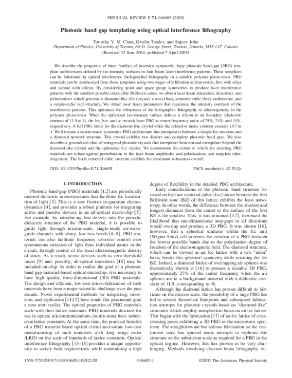
 Sajeev John