Current Opinion in Solid State and Materials Science 14 (2010) 123–130
Contents lists available at ScienceDirect
Current Opinion in Solid State and Materials Science
journal homepage: www.elsevier.com/locate/cossms
Power from plastic
Adam J. Moulé
Chemical Engineering and Materials Science Department, University of California Davis, 1 Shields Ave., Davis, CA 95616, United States
a r t i c l e
i n f o
Article history:
Received 5 February 2010
Accepted 16 June 2010
Keywords:
Polymer
Fullerene
Photovoltaic
Solar cell
a b s t r a c t
Solar power is the most abundant renewable resource on our planet. In spite of this abundance, only
0.04% of the basic power used by humans comes directly from solar sources because harvesting solar
energy using a photovoltaic (PV) panel costs more than burning fossil fuels. Solution-processable organic
materials have recently been intensively studied for PV applications, not because they show a possibility
for harvesting the sun’s power more efficiently, but because power generation from organic photovoltaic
(OPV) materials will cost considerably less than other PV technologies. The cost/Watt savings comes from
the possibility of using flexible substrates, using printable organic inks for the active layers, light-weight
transport, low temperature and ambient pressure fabrication, and reduced materials costs. The ability to
use solution processes for deposition is particularly exciting because products such as automobiles,
freight containers, and building materials could be painted with photovoltaic coatings. This article gives
an overview of the current state-of-the-art for OPV technology and discusses scientific issues that need to
be addressed to facilitate scale-up of OPV.
Ó 2010 Elsevier Ltd. All rights reserved.
1. Introduction
Use of fossil fuels is raising the levels of greenhouse gas in the
Earth’s atmosphere, which in turn threatens to cause climate
change and unknown economic hardship. Conservative calculations show that in order to avoid the largest risks for climate
change, humankind must drastically reduce the amount of primary
energy that we use on a daily basis and simultaneously shift to energy sources that result in reduced carbon emission intensity [1]. It
is well established that solar energy is by far the most abundant
source of renewable energy. However, solar energy is difficult to
harvest because it is a diffuse energy source that requires collection over large land areas and because the sun only shines during
the day. Photovoltaics are a mature technology. The first silicon
photovoltaic device was fabricated by Bell Labs in 1954. Since that
time, photovoltaics have been greatly optimized and a power conversion efficiency (PCE) approaching the Schockley–Queisser limit
for a single p/n junction of over 25% has been reported [2].
Photovoltaics only contribute �0.04% of the world’s total energy
usage [3]. The reason is that, although solar power is the most
abundant energy source, conversion of solar energy into electricity
or solar fuels is far more expensive than burning fossil fuels [1].
Government incentives to install photovoltaic capacity has resulted in growth for the solar industry of over 30% per year for
the last decade, but this growth curve is still too low to significantly reduce global greenhouse gas production, due to rising en-
E-mail address: amoule@ucdavis.edu
1359-0286/$ - see front matter Ó 2010 Elsevier Ltd. All rights reserved.
doi:10.1016/j.cossms.2010.06.003
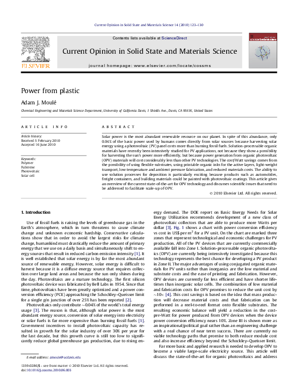
ergy demand. The DOE report on Basic Energy Needs for Solar
Energy Utilization recommends development of a new class of
photovoltaic collectors that are able to produce more Watts per
dollar [3]. Fig. 1 shows a chart with power conversion efficiency
vs cost in US$ per m2 for a PV unit. On the chart are marked three
zones that represent technological and economic challenges for PV
production. All of the PV devices that are currently commercially
available fall into Zone I. Solution-processable organic photovoltaics (OPV) are currently being intensively investigated because this
technology represents the best chance for developing a PV product
in Zone II. The major advantages of using conjugated organic materials for PV units rather than inorganics are the low material and
substrate costs and the ease of printing and fabrication. However,
OPV devices are currently far less efficient and have shorter lifetimes than inorganic solar cells. The combination of low material
and fabrication costs for OPV promises to reduce the unit cost by
�10� [4]. This cost savings is based on the idea that mass production will decrease material costs and that fabrication can be
performed in a reel-to-reel format onto flexible substrates. The
resulting economic balance will yield a reduction in the costper-Watt for power produced from OPV devices when the device
power conversion efficiency nears 10%. Zone III is shown more as
an inspirational/political goal rather than an engineering challenge
with a real chance of near term success. There are currently no
viable technology paths that promise to both reduce module cost
and also increase efficiency beyond the Schockley–Queisser limit.
Far more basic and applied research is needed to develop OPV to
become a viable large-scale electricity source. This article will
discuss the state-of-the-art for organic photovoltaics and address
�124
A.J. Moulé / Current Opinion in Solid State and Materials Science 14 (2010) 123–130
100
US$0.50/W
US$0.10/W US$0.20/W
Efficiency,%
80
Ultimate
Thermodynamic
limit
at 1 sun
60
III
US$1.00/W
40
SchockleyQueisser limit
20
0
0
100
US$3.50/W
I
II
200
300
400
500
Cost, US$/m 2
Fig. 1. PV source costs ($/Wp) as function of module efficiency and areal cost. For PV
to provide the full level of carbon-free energy required for electricity and fuel–solar
power cost needs to be �2 cents/kW h ($0.40/Wp [6]. Source: Green (2004).
scientific and technological hurdles that must be overcome for
scale-up to commercialization. A discussion of cost is found in Refs.
[5,4].
2. State-of-the-art
The first OPV device was fabricated by Tang et al. at Kodak and
had a power conversion efficiency (PCE) of 1.1%. This first device
mimicked the structure of a traditional p–n junction. It was a bilayer stack of copper phthalocyanine as the electron donor and a
perylene tetracarboxylic derivative for the electron acceptor [7].
This initial design was only able to deliver a low PCE because the
light-induced excited states (excitons) are tightly bound in organic
molecules and can only separate at donor/acceptor interfaces. Typical exciton diffusion lengths are 5–25 nm [8,9]. This small exciton
diffusion length places a fundamental limit on the thickness that a
material layer can have since light absorbed further from the interface will not result in charge separation and photocurrent.
In the early 90s a new design for OPV active layers was developed called the bulk-heterojunction (BHJ). A BHJ consists of a mixture of donor and acceptor species in the same layer [10,11]. The
layer is formed by solution casting the donor–acceptor mixture
from a common solvent. As the solvent rapidly evaporates, phase
separation occurs between the two components. The degree of
phase separation is determined by the solubility of the components in the solvent, the peed with which the film dries, and the
mutual solubility of components in each other [12,13].
The new BHJ design has the major advantage that the distance
between the donor and acceptor in the layer is reduced and the
probability of charge separation approaches unity. However, the
mixed film has reduced order, leading to reduced charge mobility,
greater trap density, and island domains that do not have a charge
transport pathway to either electrode. Until 2007, nearly all increases in OPV device PCE ultimately came about as a result improved BHJ layer morphology. For example, Shaheen et al. found
that using a solvent with improved mutual solubility for the two
components could reduce the domain size of OC1C10–PPV/[6,6]phenyl-C61–butyric acid methyl ester (PCBM) mixtures [14].
Switching from the solvent toluene to chlorobenzene improved
the PCE from 0.9% to 2.5%. Next it was discovered that the application of thermal treatment could be used to improve the hole mobility, increase crystallinity and increase efficiency in poly-3hexylthiophene (P3HT)/PCBM mixtures [15,16]. Simultaneously, it
was found that the use of high-boiling-point solvents and long sol-
vent-soaking times could optimize the morphology through self
assembly [17,18]. Finally, it was found that the morphology could
be optimized by using low-concentration additives [19] that could
improve morphology either by selectively dissolving one the components [20,21] or by causing rapid crystallization of the polymer
during drying [22,23]. All of the thermal, solvent, and additive techniques increase the PCE of a P3HT/PCBM device from �1% to >4%.
An important research theme for the last 15 years has been the
determination the mechanism for photocurrent production in a
BHJ layer. Fig. 2a shows a diagram of a BHJ device based upon
the commonly used mixture P3HT/PCBM. The mechanism for photocurrent production is depicted in Fig. 2b. Photons with energy
above the optical band gap (Eg) are absorbed in the active layer
by both the donor and acceptor materials, but since the donor
polymer has a much larger absorption coefficient, the polymer typically absorbs the majority of the light. The absorbed photons form
excitons, which for the purpose of this discussion are charge-separated excited states where both charges exist on the same species
or polymer domain. In a BHJ, the exciton has a high probability of
diffusing to a donor–acceptor interface and separating into a geminate charge pair. This geminate or bound pair, also known as a
charge-transfer exciton, consists of a Coulombically bound hole
on the donor and electron on the acceptor. The bound charge pair
can be separated into free charges at room temperature when a
sufficient electric field is applied. This built-in electric field is generated by sandwiching the BHJ layer between electrodes that have
differing work functions. Finally, the free charges can hop from
site-to-site under the influence of the built-in field until they reach
their respective electrodes. Bound charge pairs can reform from
free charges. Both bound pairs and free charges can recombine.
Fig. 2b shows a generalized relaxation pathway. The kinetics of
each process is strongly dependent on the morphology, donor/
acceptor mixing ratio, electric field, and specific donor and
(a)
LUMO offset loss
Polym
er LU
eEg
MO
Fuller
ene L
h+
UMO
Polym
High Φ
Electrode
er HO
Fuller
MO
Low Φ
Electrode
ene H
OMO
(b)
D*
δ+δ−
Exciton
A
D+ A -
+ −
E,T
Geminate Pair
D+
A-
+ ........ −
Photocurrent
Free Charges
D A
Recombination
Fig. 2. (a) Energy level diagram for an organic bulk heterojunction PV device under
short circuit conditions. (b) Cartoon of the charge-generation process: exciton
formation, dissociation into geminate pairs, and separation of the geminate pairs
into free charges under the influence of the electric field and temperature to
produce photocurrent. Geminate pairs and free charges can recombine to form
neutral species [25]. Source: Moule (2008).
�125
A.J. Moulé / Current Opinion in Solid State and Materials Science 14 (2010) 123–130
acceptor species. Blom et al. has written a detailed review of these
mechanisms [24].
Since 2007, a number of new record efficiencies have been reported that can be directly attributed to improved synthetic design
of either the donor or acceptor. Referring to Fig. 2a, three successful
synthetic strategies can be identified. First, the short circuit current
density (Jsc) can be increased by lowering the Eg and maintaining
the polymer HOMO–fullerene LUMO spacing. The second possibility is to increase the open circuit voltage Voc by maintaining the Eg
but shifting the both the HOMO and LUMO of the polymer down in
energy [26]. This shift will have the effect of lowering the energy
loss labeled LUMO offset loss in the figure. The third possibility is
to increase the Voc while maintaining the Eg by raising the LUMO
level of the fullerene. Two articles have predicted that these combined adjustments can yield power efficiencies of over 10% [27,28].
A series of new co-polymer donors have been synthesized that
use alternating electron rich and electron poor monomers. These
so-called push–pull polymers have considerably smaller Eg than
the homopolymers. Record efficiencies of 5.4% [20], 6.4% [29],
and 7.9% [30] have been reported. All of the published results used
various new push–pull polymers to achieve the high efficiencies.
Refs. [31,32] detail the synthesis and design of new donor polymers for OPV. Fullerene-based acceptors have also recently been
designed that increase the Voc of the OPV devices by adjusting up
the LUMO level of the acceptor. A bis-aduct of PCBM has been
found to increase the Voc by 0.15 V compared to the mono-aduct
[33,34]. Another acceptor, 1-(3-hexoxycarbonyl)propyl-1-phenyl[6,6]-Lu3N@C81 (Lu3N@–PCBH) uses a C80 fullerene stabilized by
a Lu3N cluster and is solubilized by a similar adduct to PCBM.
Lu3N@–PCBH yields an increase in the Voc of 0.2 V compared with
PCBM [35,36]. No work has yet appeared that uses both the new
donors and acceptors together.
The increases in PCE over the last decade came about as a result
of improved synthesis, morphology control, and a better understanding of the device physics. The synthesis achievements were
due to increased understanding of how to synthesize low-bandgap polymers and how to control the energy levels of the polymers
with respect to PCBM. However, morphology studies have been
mostly performed on OC1C10–PPV/PCBM and P3HT/PCBM mixtures. The domain size, crystallinity, and curing method (temperature, solvent soak, or solvent additive) can now be chosen for these
mixtures. A better understanding of optical and electrical loss
mechanisms has also been gained for these mixtures. But, there
is still quite a lot of academic research that needs to be performed
in all three of these areas. Hopefully, the scientific community will
have increased access to the new low-band-gap co-polymers for
morphology and device physics studies in the near future.
3. From lab bench to rooftop
In a research lab, OPV devices are fabricated in miniature to
conserve materials and to allow researchers to test the greatest
number of experimental possibilities. This experimental flexibility
leads to the practical difficulty that experimental results and efficiency records are achieved under conditions that are not scalable
to or practical for mass production of large area OPV devices. This
section will address some of the issues related to scale-up.
Fabrication of an OPV device involves four broad sequential
steps. First, a conducting substrate with an optimized work function
and surface energy is created. Second, a BHJ layer is coated onto the
substrate. Next a second electrode is deposited onto the BHJ layer.
Finally, the device is encapsulated in a material that protects the active layers from exposure to H2O, O2, and UV irradiation (Fig. 3).
As discussed in the introduction, in order for OPV to be a viable
competitor against other technologies, it is necessary to produce
Regular
Inverted
-Mask and Etch Electrode
-Clean Substrate
-Prepare Surface Layer
Prepare
Conducting
Substrate
-Coat Active Layer
-Remove Excess Solvent
Coat
Active
Layer
-Thermal Metal Evap
OR
-Coat metal NP Solution
-Remove Excess Solvent
-Sinter
Deposit
Coated
Electrode
-Apply/Coat Encapsulant
-Remove Excess Solvent
Apply
Encapsulant
-Mask Contacts
-Clean Substrate
-Prepare Surface Layer
-Coat Active Layer
-Remove Excess Solvent
-Coat Transparent Electrode
Material
-Remove Excess Solvent
-Apply/Coat Encapsulant
-Remove Excess Solvent
Fig. 3. A flow chart that shows the four sequential steps needed to fabricate an airstable OPV device for both regular and inverted fabrication.
OPV at minimal cost. The fabrication will be discussed assuming
a reel-to-reel fabrication. OPV devices can either be regular (i.e.
holes move towards the substrate) or inverted (i.e. holes move
away from the substrate). The direction of current flow is determined by the choice of electrode materials. One of the requirements for reel-to-reel coating is that the substrate be flexible so
that it can be pulled through the reels. Regular devices can be fabricated onto transparent plastic foils that have been coated with a
transparent conducting oxide (TCO) such as ITO, ZnO:Al or SnO2:F.
The first step for fabrication has been shaded in Fig. 3 because
highly conducting and transparent TCO materials are crystalline,
not flexible, and will crack when drawn through bends with a
low radius of curvature [37,38]. Cracks in the TCO degrade electrical performance of a device significantly. The shading indicates
that this topic requires considerable innovation. An inverted device
can either be coated onto a metal foil or onto a preformed metal
part. Preparation of the substrate electrode requires similar steps
for both device types. First the electrode must be either etched into
the required shape or a resistive coating must be applied to prevent shorts where the electrodes will be externally contacted. Then
the substrate material must be extensively cleaned and the
electrode materials coated with a layer of material that sets the
work function. Poly(3,4-ethylenedioxythiophene):poly(styrenesulfonate) (PEDOT:PSS) is commonly used on top of ITO for a hole contact for regular devices. TiOx[39], ZnO [40], and Ca2CO3 [41] have
all been investigated as electron contact interlayer materials.
The second step is coating of the active layer mixture. This step
is performed identically for both device types. The only difference
that could arise in the film comes from possible differences in morphology. Since regular and inverted devices have differing electrodes the surface energies of the prepared substrates could be
different. This difference in surface energy could lead to differing
surface driven formation of morphology features. If the outer surface of the substrates have differing surface energies, the coating
conditions must be adjusted to achieve similar layer thickness
and dry morphology. For both device types, excess solvent must
be driven from the BHJ film to ensure morphological stability [42].
Next comes the coated electrode. This step is marked in dark
gray in Fig. 3 because this is the area that requires the most innovation for both device types. In the case of a regular device, a metal
electrode must be deposited. A metal is always chosen for the back
electrode material because it reflects transmitted light back
through the active layer and thereby increases light absorption
and photocurrent. Thermal evaporation of a metal is used in a research lab for electrode deposition. Thermal evaporation requires
�126
A.J. Moulé / Current Opinion in Solid State and Materials Science 14 (2010) 123–130
small device areas and high vacuum conditions that are not compatible with reel-to-reel fabrication. Solution methods have been
developed for printing a �50 lm Ag wire mesh from solution onto
various substrates [43,37,?]. The disadvantage of this technique is
that the Ag mesh has reduced transparency compared to a TCO and
the ‘‘windows” between the Ag wires also have to be filled with a
transparent conductor to move charges to the wires and to planarize the Ag mesh. Low-temperature deposition of a transparent
conducting electrode for an inverted device is even more difficult
because oxides and conducting polymers have lower conductivity
and are more complex materials than metals. For both device
types, heat treatments must remain below 200 °C to prevent damage to the BHJ material.
Finally, an encapsulant material must be applied that blocks O2,
H2O, and UV radiation from the active layer material. The requirements of the encapsulant materials are that it be transparent, flexible, durable, impermeable, and low-cost. The deposition should
also not destroy any of the layers already deposited and should
not require curing temperatures above 200 °C. For this step, solution-based or lamination-based application of the encapsulant
layer are preferable. Also for this step, the application should be
identical for both device types.
3.1. Substrates
The prerequisite for an OPV substrate material is that it be
highly conducting. As discussed above, the substrate can either
be a metal or a transparent conductor. Research lab OPV devices
are typically fabricated on indium–tin oxide (ITO) coated glass substrates that are cut and etched to a predetermined size and shape.
For both regular and inverted device types, transparent ITO coated
polyethylene terephthalate (PET) substrates can also be used as a
substrate material. The PET substrate has the significant advantage
that it is flexible, and so is compatible with a reel-to-reel coating
technique. However, ITO coated onto PET has been shown to develop cracks upon bending that leads to significant reduction in the
conductivity of the substrate [37].
In general, TCO electrode materials that are suitable for electrodes have crystalline domains that are likely to be brittle and
perform poorly after bending. For this reason, a number of groups
are working on transparent electrode materials based on organic
components. Single walled carbon nanotubes (CNT) have been
studied for use as a transparent electrode material [45,46]. However, CNTs are synthesized as a mixture of semiconducting and
metalic tubes. Schottky contacts form at junctions between the
semiconducting and metalic tubes that cause significant reductions in conductivity, resulting in high sheet resistance [47]. A second approach is to replace the TCO with a graphene-based
composite [48,49]. This approach leads to high sheet-resistance
electrodes and is much too expensive with the current high price
of graphene. A number of groups have used a doped conjugated
polymer, such as highly doped PEDOT:PSS, to replace the TCO
[50–52]. The conductivity of PEDOT:PSS is lower than that of most
TCOs and so the resulting devices have reduced filling factor. Nevertheless, OPV devices with a PEDOT:PSS electrode based on P3HT/
bis-PCBM has been reported with a PCE of 3.5% [53]. Another approach to making an electrode transparent is to fabricate a nanoscale metal mesh with most of the area being transparent. OPV
devices have been fabricated based on Ag nanowire meshes that
show promising efficiency [43,44]. A recent article looked at the
relationship between series resistance (Rs) that comes from the
substrate itself and IV characteristics of OPV devices. They found
that low Rs is critical for maintaining a high FF and PCE, especially
as device area is increased [54].
A second and essential function of the electrode in OPV devices
is charge selectivity. A metal can be chosen that has a work func-
tion of that matches either the HOMO or LUMO of the BHJ mixture,
but because metals have unfilled densities of states able the fermi
level and because they form large dipoles on their surfaces when
organic materials are added, metal electrodes have poor charge
selectivity [55,56]. Thin (typically <100 nm) layers of various semiconductor materials are used to create charge selectivity. These
layers are known as interlayers, hole/electron transport layers or
hole/electron-only layers. For regular devices, PEDOT-PSS is spin
coated to make the hole-collecting electrode selective [57]. It has
also been shown that PEDOT:PSS also alters the wettability of the
substrate to the polymer and thereby increases charge transport
[58]. V2O5 [41,59], NiO [60], and other cross-linkable hole conducting polymers [61] have also been used as to create hole selective
electrodes. These replacements for PEDOT:PSS have been reported
to be more thermally stable and thereby, should lead to longer device lifetimes. However all record efficiencies have been posted
using PEDOT:PSS. For inverted devices a solgel of TiO2 [39,62,63],
ZnO [40,64–66], Cs2CO3 [41,67,59], or conjugated polyelectrolite[68] is coated onto the ITO surface to make an electron selective
contact. Several recent review articles cover the fabrication and
function of interlayers that are used for regular and inverted devices [69–71]. The thin electrode coatings listed above have very
small crystalline domains and are therefore resistant to cracking
upon mechanical stress. The small domain sizes also lead to much
higher sheet resistances than ITO. So these coating materials are
not suitable for complete transparent electrodes.
In the introduction it was stressed that one major advantage of
OPV technology is that it is compatible with flexible substrates. In
fact, the coating of BHJ layers can conceivably be controlled better
using a reel-to-reel coating technique rather than spin coating. This
discussion of research into substrate materials reveals that all efficiency records have been recorded using ITO coated with PEDOT:PSS as the transparent electrode in spite of the fact that ITO
has been widely predicted to be too expensive [72] and has been
shown to perform very poorly in mechanical stress tests [37]. PEDOT:PSS is also not ideal for use in an OPV device because it is highly
acidic [42,73,74] and thought to be a source of degradation in the
active layer [25]. It is therefore extremely important that a strong
and dedicated research emphasis be placed on the development
and characterization of new transparent electrode materials that
are compatible with OPV fabrication conditions.
3.2. Coating
In a lab setting, BHJ layers are typically formed using spin coating. Spin coating is a batch coating method that requires that each
individual small-area substrate be loaded and coated separately.
The spin-coating technique does not effectively scale-up to largearea coating. A more cost-effective alternative is to use flexible
substrates that can be coated using a reel-to-reel technique in
which the substrate is passed through a series of reels and the layers are sequentially coated using a compatible coating technique.
Several groups have started working on reel-to-reel coating
methods for OPVs. They have developed an inkjet printing
(Fig. 4a) techniques for P3HT/PCBM BHJ layers on regular electrodes that yielded power conversion efficiencies of over 3% [75–
77]. The authors reported that the morphology formed from inkjet
printing is distinctly different than from spin-coated or doctorbladed layers [78]. This result suggests that the current practice
of studying the morphology of BHJ devices fabricated from spin
coating may yield scientific data that is not technically relevant
for the coating techniques most likely to be used. Shaheen et al.
have used screen printing (Fig. 4b) to coat OC1C10–PPV/PCBM
OPV devices [79]. Kim et al. have used a brush coating technique
to coat P3HT/PCBM layers. They found that the PCE is highly
dependent upon the substrate temperature during coating. A high
�A.J. Moulé / Current Opinion in Solid State and Materials Science 14 (2010) 123–130
127
Fig. 4. Schematic diagrams of (a) inkjet printing [76], (b) screen printing [79], (c) spray coating [81], and (d) slot die coater heads for single and multiple layers [42].
coating temperature led to phase separation on a larger length
scale [80]. A likely coating technique to be used for industrial
scale-up of BHJ printing onto flexible substrates is slot-die coating
(Fig. 4d) [42,73,74]. Slot-die coating has the advantages of being
amenable to reel-to-reel printing, it is a metered coating technique,
which means that no ink is lost, and either single or multiple layers
can be coated.
Reel-to-reel coating methods are useful for coating onto flexible
substrates, which should be an advantage of OPV technology since
the active layer film is highly flexible. However, for many applications a flexible substrate is not suitable. For example if an OPV
coating is to be used as a photovoltaic replacement for automobile
paint, the BHJ layer would have to be coated onto the ridged and
curved pieces of an auto body. For this application, a spray coating
(Fig. 4c) technique is more appropriate. Several groups have spray
coated OPV devices onto glass/ITO substrates and achieved PCEs of
over 3% [82,83,81,84–87]. The main issues for spray-coating appear
to be formation of sufficiently small droplets, wetting of the substrate, film drying rate, containing airborn solvent, and reducing
the surface tension of the ink.
3.3. Coated electrodes
For a functional OPV device, the active OPV layer is sandwiched
between two electrodes and one of the electrodes must be transparent. These requirements mean that the second electrode must
be deposited on top of the active OPV layer. Since the active layer
is made from a polymer, the deposition technique must be compatible with low temperatures, to prevent damage, and/or hydrophilic
solvents that will not redissolve the polymer layer. The need for a
low-temperature deposition technique means that sputtering cannot be used on the polymer because the sputtered material will
burn the organic upon deposition. However, if an oxide layer is
deposited using a sol–gel, then a metal can be sputtered on top.
In a research lab, the back electrode for a regular device is typically
deposited by a metal evaporation source in high vacuum condi-
tions. The metal must be evaporated at a rate 61 nm/s or the polymer can be burned [40]. Evaporation requires a vacuum source and
is time consuming, which makes it a poor technique choice for
high-speed and low-cost production of OPV devices. Ideally, a solution processing method should exist for the deposition of metal
electrodes. The current best alternative to evaporation is to coat
a suspension of metal nanoparticles (commercially available) and
create a low conductivity porous electrode. Again because of the
restriction that temperatures over 200 °C cannot be used to avoid
damage to the OPV layer, the metal particle layer cannot be sintered to increase the connectivity between the particles. A more
attractive solution for metal electrode deposition currently does
not exist. One interesting advantage of the deposition of metal
nanoparticles for electrodes is that the deposition technique is
compatible with spray-coating conditions [88].
Deposition of transparent electrodes for inverted devices is
more difficult. TCO materials such as ITO, ZnO, and SnO2:F can all
be deposited using sputtering techniques, but as discussed above,
these techniques can burn the underlying OPV material. In addition, sputtering requires a vacuum and cannot be performed continuously in a reel-to-reel deposition. Sol–gel methods exist to
deposit some oxides, such as TiO2, but the resulting layers have
much too high a sheet resistance to be used as the electrode material. In the section on substrates, we identified several alternatives
for deposition of transparent electrodes, including CNTs, highly
doped conjugated polymers, and Ag nanowire meshes. Deposition
of the top electrode is more difficult because not only must the
requirements of transparency and conductivity be met for the
top electrode but the material must also be prepared in a form that
can easily be coated from a solution in a reel-to-reel fabrication
onto a low surface energy film. These very high requirements make
the development of a coatable transparent electrode material the
most difficult challenge for mass production of OPV devices. If such
an electrode material can be developed, it will open the way for the
development of truely transformational technologies such as photovoltaic car and building paints.
�128
A.J. Moulé / Current Opinion in Solid State and Materials Science 14 (2010) 123–130
3.4. Encapsulating materials
Acknowledgements
Most research on OPV devices is performed in N2 gloveboxes. It
is well known that OPV devices will degrade quickly on exposure
to air. The mechanisms for degradation follow three known pathways. First, the metal electrode is typically a low work-function
metal that oxidizes on exposure to O2 or H2O [89,90]. Second, if
O2 is present in the active layer, it can be photo excited to singlet
�
oxygen O�2 which reacts with and bleaches the polymer. Third,
upon exposure to long-term heating, the active layer can phase
separate [91]. Both of the first two degradation mechanisms can
be avoided if the O2 and H2O levels can be kept sufficiently low.
However, the sensitivity of organic electronic materials to O2 is
very high. O2 levels in the active layer must be kept four-ordersof-magnitude lower than can be attained using typical food packaging encapsulants [92]. Several groups have focused research efforts on creating solution-processable transparent encapsulant
barriers that are based on a mixture of clay pellets and polymers
[93]. Several groups have also published results that show OPV device lifetimes greater than several thousand hours, but unfortunately the identity of the encapsulant material is usually not
disclosed [92,94,95]. The study of lifetime in OPV devices is particularly difficult because devices are very complicated, layered, and
the defect states are below the limit of detection for most optical
detection techniques. There is some evidence that defect states
form at the metal electrode surface even in dark oxidant-free conditions [96]. In conclusion, it appears that encapsulant materials
suitable for OPV applications have been developed though the
identity of the materials is intellectual property. On the other hand
there is not enough known about the basic mechanisms behind
OPV device degradation. This author recommends much more basic research on the applied problem of lifetime enhancement in
OPV devices with a particular emphasis on studying interfaces between layers and developing measurement techniques that are
sensitive to interface states at burried interfaces.
The writing of this article was funded by the California Solar Energy Collaborative and the United States Department of Energy under Grant No. DE-FG3608GO18018. Thanks to my group members
David Huang, Scott Mauger, John Roehling, Lilian Chang, and Chris
Rochester for editing.
4. Conclusions
Organic photovoltaics is a facinating subject to study. It is necessary to be familiar with optical absorption processes, charge
transport, polymer morphology, recombination kinetics, the relationship between polymer structure and electronic and optical
properties, the interaction between metal and organic layers, and
a host of other interesting basic science themes. The increase in
the power conversion efficiency of organic photovoltaics from
<2% to 7.9% in eight years is mostly due to intense and focused academic research on the basic science issues surrounding every aspect of this device type.
In the past 2–3 years several companies have started to produce
OPV materials and have reported record PCEs that cannot be
matched by academic groups. This is, however, not the right time
for reduced governmental support of academic research in this
area. In fact much more research is needed. This review article
has focused on the scale-up of OPV to a reel-to-reel solution-processed and mass-produced product. Almost the entire article stresses that research must still be done on flexible transparent
electrodes, solution-processable electrodes (metal or transparent),
developing reel-to-reel and spray coating methods, studying polymer morphology that results from the new coating methods, developing effective transparent O2 and H2O barrier materials, and
learning to make all of these technologies work together. Largescale production and distribution of low-cost OPV modules can
play an important role in greenhouse gas reduction and meeting
global energy demands. These goals are urgent and need to be addressed by increased funding of basic and applied research in this
area.
References
[1] Lewis NS. Powering the planet. MRS Bull 2007;32:808–20.
[2] Green MA, Emery K, Hishikawa Y, Warta W. Solar cell efficiency tables (version
34). Prog Photovolt 2009;17(5):320–6.
[3] Basic research needs for solar energy utilization. Technical Report, Department
of Energy; 2005.
[4] Brabec CJ, Hauch JA, Schilinsky P, Waldauf C. Production aspects of organic
photovoltaics and their impact on the commercialization of devices. MRS Bull
2005;30(1):50–2.
[5] Brabec CJ. Organic photovoltaics: technology and market. Sol Energy Mater Sol
Cells 2004;83(2–3):273–92.
[6] Green MA. Third generation photovoltaics: advance solar energy
conversion. Springer-Verlag; 2003.
[7] Tang CW. 2-Layer organic photovoltaic cell. Appl Phys Lett 1986;48(2):183–5.
[8] Markov DE, Amsterdam E, Blom PWM, Sieval AB, Hummelen JC. Accurate
measurement of the exciton diffusion length in a conjugated polymer using a
heterostructure with a side-chain cross-linked fullerene layer. J Phys Chem A
2005;109(24):5266–74.
[9] Barker JA, Ramsdale CM, Greenham NC. Modeling the current–voltage
characteristics of bilayer polymer photovoltaic devices. Phys Rev B
2003;67(7):075205.
[10] Yu G, Gao J, Hummelen JC, Wudl F, Heeger AJ. Polymer photovoltaic cells—
enhanced efficiencies via a network of internal donor–acceptor
heterojunctions. Science 1995;270(5243):1789–91.
[11] Neuteboom EE, Meskers SCJ, van Hal PA, van Duren JKJ, Meijer EW, Janssen
RAJ, et al. and photovoltaic properties of a new class of donor–acceptor
materials. J Am Chem Soc 2003;125(28):8625–38.
[12] Hoppe H, Sariciftci NS. Morphology of polymer/fullerene bulk heterojunction
solar cells. J Mater Chem 2006;16(1):45–61.
[13] Kim JY, Frisbie D. Correlation of phase behavior and charge transport in
conjugated polymer/fullerene blends. J Phys Chem C 2008;112(45):17726–36.
[14] Shaheen SE, Brabec CJ, Sariciftci NS, Padinger F, Fromherz T, Hummelen JC,
et al. Appl Phys Lett 2001;78(6):841–3.
[15] Padinger F, Rittberger RS, Sariciftci NS. Effects of postproduction treatment on
plastic solar cells. Adv Funct Mater 2003;13(1):85–8.
[16] Ma W, Yang C, Gong X, Lee K, Heeger AJ, stable Thermally. efficient polymer
solar cells with nanoscale control of the interpenetrating network
morphology. Adv Funct Mater 2005;15:1617–22.
[17] Li G, Shrotriya V, Huang J, Yao Y, Moriarty T, Emery K, et al. High-efficiency
solution processable polymer photovoltaic cells by self-organization of
polymer blends. Nat Mater 2005;4:864–8.
[18] Li G, Yao Y, Yang H, Shrotriya V, Yang G, Yang Y. Solvent annealing effect in
polymer solar cells based on poly(3-hexylthiophene) and methanofullerenes.
Adv Funct Mater 2007;17(10):1636–44.
[19] Zhang FL, Jespersen KG, Bjorstrom C, Svensson M, Andersson MR, Sundstrom V,
et al. Influence of solvent mixing on the morphology and performance of solar
cells based on polyfluorene copolymer/fullerene blends. Adv Funct Mater
2006;16(5):667–74.
[20] Peet J, Kim JY, Coates NE, Ma WL, Moses D, Heeger AJ, et al. Efficiency
enhancement in low-bandgap polymer solar cells by processing with alkane
dithiols. Nat Mater 2007;6(7):497–500.
[21] Lee JK, Ma WL, Brabec CJ, Yuen J, Moon JS, Kim JY, et al. Processing additives for
improved efficiency from bulk heterojunction solar cells. J Am Chem Soc
2008;130(11):3619–23.
[22] Moulé AJ, Meerholz K. Controlling morphology in polymer–fullerene mixtures.
Adv Mater 2008;20(2):240–5.
[23] Moulé AJ, Meerholz K. Morphology control in solution-processed bulkheterojunction solar cell mixtures. Adv Funct Mater 2009;19:3028–36.
[24] Blom PWM, Mihailetchi VD, Koster LJA, Markov DE. Device physics of polymer:
fullerene bulk heterojunction solar cells. Adv Mater 2007;19(12):1551–66.
[25] Moulé AJ, Meerholz K. Intensity-dependent photocurrent generation at the
anode in bulk-heterojunction solar cells. Appl Phys B: Lasers Opt
2008;92(2):209–18.
[26] Kooistra FB, Knol J, Kastenberg F, Popescu LM, Verhees WJH, Kroon JM, et al.
Increasing the open circuit voltage of bulk-heterojunction solar cells by raising
the LUMO level of the acceptor. Org Lett 2007;9(4):551–4.
[27] Koster LJA, Mihailetchi VD, Blom PWM. Ultimate efficiency of polymer/
fullerene bulk heterojunction solar cells. Appl Phys Lett 2006;88(9):093511.
[28] Scharber MC, Wuhlbacher D, Koppe M, Denk P, Waldauf C, Heeger AJ, et al.
Design rules for donors in bulk-heterojunction solar cells—towards 10%
energy-conversion efficiency. Adv Mater 2006;18(6):789–94.
[29] http://www.konarka.com/index.php/site/pressreleasedetail/national_energy_
renewable_laboratory_nrel_certifies_konarkas_photovoltaic_s. National
�A.J. Moulé / Current Opinion in Solid State and Materials Science 14 (2010) 123–130
[30]
[31]
[32]
[33]
[34]
[35]
[36]
[37]
[38]
[39]
[40]
[41]
[42]
[43]
[44]
[45]
[46]
[47]
[48]
[49]
[50]
[51]
[52]
[53]
[54]
[55]
[56]
[57]
[58]
[59]
[60]
Renewable Energy Laboratory (NREL) certifies Konarkas photovoltaic solar
cells at 6.4.
http://www.pvtech.org/news/_a/solarmer_breaks_organic_solar_pv_cell_
conversion_efficiency_record_hits_nre/. Solarmer breaks organic solar PV cell
conversion efficiency record, hits NREL-certification, website; December 2009.
Kroon R, Lenes M, Hummelen JC, Blom PWM, De Boer B. Small bandgap
polymers for organic solar cells (polymer material development in the last 5
years). Polym Rev 2008;48(3):531–82.
Thompson BC, Frechet JMJ. Organic photovoltaics–polymer–fullerene
composite solar cells. Angew Chem Int Ed 2008;47(1):58–77.
Lenes M, Wetzelaer G-JAH, Kooistra FB, Veenstra SC, Hummelen JC, Blom
PWM. Fullerene bisadducts for enhanced open-circuit voltages and efficiencies
in polymer solar cells. Adv Mater 2008;20(11):2116–9.
Martijn L, Steve WS, Alex BS, David FK, Jan CH, Paul WMB. Electron trapping in
higher adduct fullerene-based solar cells. Adv Funct Mater 2009;19(18):
3002–7.
Ross RB, Cardona CM, Guldi DM, Sankaranarayanan SG, Reese MO, Kopidakis N,
et al. Endohedral fullerenes for organic photovoltaic devices. Nat Mater
2009;8(3):208–12.
Ross RB, Cardona CM, Swain FB, Guldi DM, Sankaranarayanan SG, Van Keuren
E, et al. Tuning conversion efficiency in metallo endohedral fullerene-based
organic photovoltaic devices. Adv Funct Mater 2009;19(14):2332–7.
Krebs F. Polymer photovoltaics: a practical approach. SPIE Press; 2008.
Paetzold R, Heuser D, Henseler K, Roeger S, Wittmann G, Winnacker A.
Performance of flexible polymeric light-emitting doedes under bending
conditions. Appl Phys Lett 2003;82(19).
Waldauf C, Morana M, Denk P, Schilinsky P, Coakley K, Choulis SA, et al. Highly
efficient inverted organic photovoltaics using solution based titanium oxide as
electron selective contact. Appl Phys Lett 2006;89(23).
White MS, Olson DC, Shaheen SE, Kopidakis N, Ginley DS. Inverted bulkheterojunction organic photovoltaic device using a solution-derived ZnO
underlayer. Appl Phys Lett 2006;89(14).
Li G, Chu CW, Shrotriya V, Huang J, Yang Y. Efficient inverted polymer solar
cells. Appl Phys Lett 2006;88(25).
Krebs FC. Fabrication and processing of polymer solar cells: a review of printing
and coating techniques. Sol Energy Mater Sol Cells 2009;93(4):394–412.
Tvingstedt K, Inganas O. Electrode grids for ITO-free organic photovoltaic
devices. Adv Mater 2007;19(19):2893.
Lee J-Y, Connor ST, Cui Y, Peumans P. Solution-processed metal nanowire mesh
transparent electrodes. Nano Lett 2008;8(2):689–92. doi:10.1021/nl073296g.
Wu ZC, Chen ZH, Du X, Logan JM, Sippel J, Nikolou M, et al. conductive carbon
nanotube films. Science 2004;305(5688):1273–6.
Rowell MW, Topinka MA, McGehee MD, Prall HJ, Dennler G, Sariciftci NS, et al.
Organic solar cells with carbon nanotube network electrodes. Appl Phys Lett
2006;88(23).
Topinka MA, Rowell MW, Goldhaber-Gordon D, McGehee MD, Hecht DS,
Gruner G. Charge transport in interpenetrating networks of semiconducting
and metallic carbon nanotubes. Nano Lett 2009;9(5):1866–71.
Stankovich S, Dikin DA, Dommett GHB, Kohlhaas KM, Zimney EJ, Stach EA,
et al. Graphene-based composite materials. Nature 2006;442(7100):282–6.
Wu J, Becerril HA, Bao Z, Liu Z, Chen Y, Peumans P. Organic solar cells with
solution-processed graphene transparent electrodes. Appl Phys Lett
2008;92(26):263302–3.
Yinhua Z, Fengling Z, Kristofer T, Sophie B, Fenghong L, Wenjing T, et al.
Investigation on polymer anode design for flexible polymer solar cells. Appl
Phys Lett 2008;92(23):233308.
Huang J, Wang X, Kim Y, deMello AJ, Bradley DDC, Demello JC. High efficiency
flexible ITO-free polymer/fullerene photodiodes. Phys Chem Chem Phys
2006;8(33):3904–8.
Hau SK, Yip H-L, Zou J, Jen AKY. Indium tin oxide-free semi-transparent
inverted polymer solar cells using conducting polymer as both bottom and top
electrodes. Org Electron 2009;10(7):1401–7.
Do H, Reinhard M, Vogeler H, Puetz A, Klein MFG, Schabel W, et al. Thin Solid
Films 2009;517(20):5900–2.
Harding MJ, Poplavskyy D, Choong V-E, So F, Campbell AJ. Variations in hole
injection due to fast and slow interfacial traps in polymer light-emitting
diodes with interlayers. Adv Funct Mater 2010;20(1):119–30.
Mihailetchi VD, Blom PWM, Hummelen JC, Rispens MT. Cathode dependence
of the open-circuit voltage of polymer: fullerene bulk heterojunction solar
cells. J Appl Phys 2003;94(10):6849–54.
Braun S, Salaneck WR, Fahlman M. Energy-level alignment at organic/metal
and organic/organic interfaces. Adv Mater 2009;21(14–15):1450–72.
Frohne H, Shaheen SE, Brabec CJ, Muller DC, Sariciftci NS, Meerholz K.
Influence of the anodic work function on the performance of organic solar
cells. ChemPhysChem 2002;3(9):795–9.
Mitchell WJ, Burn PL, Thomas RK, Fragneto G, Markham JPJ, Samuel IDW.
Relating the physical structure and optical properties of conjugated polymers
using neutron reflectivity in combination with photoluminescence
spectroscopy. J Appl Phys 2004;95(5).
Liao HH, Chen LM, Xu Z, Li G, Yang Y. Highly efficient inverted polymer solar
cell by low temperature annealing of Cs2CO3 interlayer. Appl Phys Lett
2008;92(17).
Irwin MD, Buchholz B, Hains AW, Chang RPH, Marks TJ, et al. p-type
semiconducting nickel oxide as an efficiency-enhancing anode interfacial
layer in polymer bulk-heterojunction solar cells. Proc Natl Acad Sci USA
2008;105(8):2783–7.
129
[61] Hains AW, Liu ABF, Martinson J, Irwin MD, Marks TJ. Anode interfacial tuning
via electron-blocking/hole transport layers and indium tin oxide surface
treatment in bulk-heterojunction organic photovoltaic cells. J Mater Chem
2010;20:595–606.
[62] Yoshikawa O, Fujieda T, Uehara K, Yoshikawa S. High performance
polythiophene/fullerene bulk-heterojunction solar cell with a TiOx hole
blocking layer. Appl Phys Lett 2007;90:163517.
[63] Bouclé J, Ravirajan P, Nelson J. Hybrid polymer–metal oxide thin films for
photovoltaic applications. J Mater Chem 2007;17:3141–53.
[64] Olson DC, Lee Y-J, White MS, Kopidakis N, Shaheen SE, Ginley DS, et al. Effect of
ZnO processing on the photovoltage of ZnO/poly(3-hexylthiophene) solar cells.
J Phys Chem C 2008;112(26):9544–7.
[65] Yip HL, Hau SK, Baek NS, Ma H, Jen AKY. Polymer solar cells that use selfassembled-monolayer-modified ZnO/metals as cathodes. Adv Mater
2008;20(12):2376. –+ [times cited: 2].
[66] Yip HL, Hau SK, Baek NS, Jen AKY. Self-assembled monolayer modified ZnO/
metal bilayer cathodes for polymer/fullerene bulk-heterojunction solar cells.
Appl Phys Lett 2008;92(19) [times cited: 3].
[67] Huang YYJ, Xu Z. Low-work-function surface formed by solution-processed
and thermally deposited nanoscale layers of cesium carbonate. Adv Funct
Mater 2007;17(12):1966–73. doi:10.1002/adfm.200700051.
[68] He C, Zhong C, Yang R, Yang R, Huang F, Bazan GC, et al. Origin of the enhanced
open-circuit voltage in polymer solar cells via interfacial modification using
conjugated polyelectrolytes. J Mater Chem 2010;20:2617–22.
[69] Chen LM, Xu Z, Hong Z, Yang Y. Interface investigation and engineering—
achieving high performance polymer photovoltaic devices. J Mater Chem
2010;20:2575–98.
[70] Steim R, Brabec CJ. Interface materials for organic solar cells. J Mater Chem
2010;20:2499–512.
[71] Ma H, Yip H-L, Huang F, Jen AK-Y. Interface engineering for organic electronics.
Adv Funct Mater 2010;20:1371–88.
[72] Yang F, Forrest SR. Organic solar cells using transparent SnO2-f anodes. Adv
Mater 2006;18(15):2018.
[73] Krebs FC. Polymer solar cell modules prepared using roll-to-roll methods:
knife-over-edge coating, slot-die coating and screen printing. Sol Energy Mater
Sol Cells 2009;93(4):465–75.
[74] Krebs FC, Jorgensen M, Norrman K, Hagemann O, Alstrup J, Nielsen TD, et al. A
complete process for production of flexible large area polymer solar cells
entirely using screen printing—first public demonstration. Sol Energy Mater
Sol Cells 2009;93(4):422–41.
[75] Xia YJ, Friend RH. Polymer bilayer structure via inkjet printing. Appl Phys Lett
2006;88(16):163508.
[76] Hoth CN, Choulis SA, Schilinsky P, Brabec CJ. High photovoltaic performance of
inkjet printed polymer: fullerene blends. Adv Mater 2007;19(22):3973–8.
[77] Hoth CN, Schilinsky P, Choulis SA, Brabec CJ. Printing highly efficient organic
solar cells. Nano Lett 2008;8(9):2806–13.
[78] Schilinsky P, Waldauf C, Brabec C. Performance analysis of printed bulk
heterojunction solar cells. Adv Funct Mater 2006;16:1669–72.
[79] Shaheen SE, Radspinner R, Peyghambarian N, Jabbour GE. Fabrication of bulk
heterojunction plastic solar cells by screen printing. Appl Phys Lett
2001;79(18):2996–8.
[80] Kim S-S, Na S-I, Jo J, Tae G, Kim D-Y. Efficient polymer solar cells fabricated by
simple brush painting. Adv Mater 2007;19:4410–5.
[81] Steirer KX, Reese MO, Rupert BL, Kopidakis N, Olson DC, Collins RT, et al.
Ultrasonic spray deposition for production of organic solar cells. Sol Energy
Mater Sol Cells 2009;93(4):447–53.
[82] Treossi E, Liscio A, Feng XL, Palermo V, Mullen K, Samori P. Large-area bicomponent processing of organic semiconductors by spray deposition and
spin coating with orthogonal solvents. Appl Phys A—Mater Sci Process
2009;95(1):15–20.
[83] Hoth CN, Steim R, Schilinsky P, Choulis SA, Tedde SF, Hayden O, et al.
Topographical and morphological aspects of spray coated organic
photovoltaics. Org Electron 2009;10(4):587–93.
[84] Girotto C, Rand BP, Genoe J, Heremans P. Exploring spray coating as a
deposition technique for the fabrication of solution-processed solar cells. Sol
Energy Mater Sol Cells 2009;93(4):454–8.
[85] Vak D, Kim S-S, Jo J, Oh S-H, Na S-I, Kim J, et al. Fabrication of organic bulk
heterojunction solar cells by a spray deposition method for low-cost power
generation. Appl Phys Lett 2007;91(8):081102.
[86] Green R, Morfa A, Ferguson AJ, Kopidakis N, Rumbles G, Shaheen SE.
Performance of bulk heterojunction photovoltaic devices prepared by
airbrush spray deposition. Appl Phys Lett 2008;92(3):033301–3.
[87] Ishikawa T, Nakamura M, Fujita K, Tsutsui T. Preparation of organic bulk
heterojunction photovoltaic cells by evaporative spray deposition from
ultradilute solution. Appl Phys Lett 2004;84(13):2424–6.
[88] Hau SK, Yip H-L, Leong K, Jen AKY. Spraycoating of silver nanoparticle
electrodes for inverted polymer solar cells. Org Electron 2009;10(4):719–23.
[89] Kim JB, Kim CS, Kim YS, Loo YL. Oxidation of silver electrodes induces
transition from conventional to inverted photovoltaic characteristics in
polymer solar cells. Appl Phys Lett 2009;95(18).
[90] Reese MO, White MS, Rumbles G, Ginley DS, Shaheen SE. Optimal negative
electrodes for poly(3-hexylthiophene): [6,6]-phenyl c61-butyric acid methyl
ester bulk heterojunction photovoltaic devices. Appl Phys Lett 2008;92(5).
[91] Chirvase D, Parisi J, Hummelen JC, Dyakonov V. Influence of nanomorphology
on the photovoltaic action of polymer–fullerene composites. Nanotechnology
2004;15(9):1317–23.
�130
A.J. Moulé / Current Opinion in Solid State and Materials Science 14 (2010) 123–130
[92] Dennler G, Lungenschmied C, Neugebauer H, Sariciftci NS, Latreche M,
Czeremuszkin G, et al. A new encapsulation solution for flexible organic
solar cells. Thin Solid Films 2006;511:349–53.
[93] Ebina T, Mizukami F. Flexible transparent clay films with heat-resistant and
high gas-barrier properties. Adv Mater 2007;19(18):2450–3.
[94] Houch JA, Schilinsky P, Choulis SA, Rajoelson S, Brabec CJ. The impact of water
vapor transmission rate on the lifetime of flexible poly solar cells. Appl Phys
Lett 2008;93:103306.
[95] Lungenschmied C, Dennler G, Neugebauer H, Sariciftci SN, Glatthaar M,
Meyer T, et al. organic solar cells. Sol Energy Mater Sol Cells 2007;91(5):379–
84.
[96] Reese MO, Morfa AJ, White MS, Kopidakis N, Shaheen SE, Rumbles G, et al.
Pathways for the degradation of organic photovoltaic p3ht:Pcbm based
devices. Sol Energy Mater Sol Cells 2008;92(7):746–52.
�
 Adam Moulé