Academia.edu no longer supports Internet Explorer.
To browse Academia.edu and the wider internet faster and more securely, please take a few seconds to upgrade your browser.
Nano-focusing in an Air-slot Plasmonic Waveguide With a Tapered Grating Coupler
Nano-focusing in an Air-slot Plasmonic Waveguide With a Tapered Grating Coupler
 Nicolás Abadía
2016, Conference on Lasers and Electro-Optics
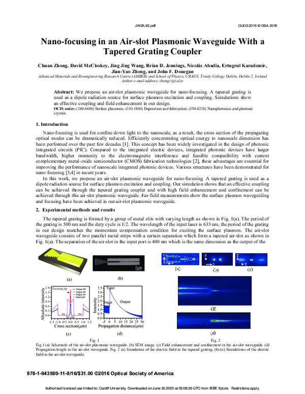
We propose an air-slot plasmonic waveguide for nano-focusing. A tapered grating is used as a dipole radiation source for surface plasmon excitation and coupling. Simulations show an effective coupling and field enhancement in our design.
Related Papers
Nature Photonics
Nanofocusing in a metal–insulator–metal gap plasmon waveguide with a three-dimensional linear taper2012 •
Applied Physics Letters
Adiabatic and nonadiabatic nanofocusing of plasmons by tapered gap plasmon waveguides2006 •
2005 •
The constructive interference of surface plasmon polaritons (SPP) launched by nanometric holes allows us to focus SPP into a spot of high near-field intensity having subwavelength width. Near-field scanning optical microscopy is used to map the local SPP intensity. The resulting SPP patterns and their polarization dependence are accurately described in model calculations based on a dipolar model for the SPP emission at each hole. Furthermore, we show that the high SPP intensity in the focal spot can be launched and propagated on a Ag strip guide with a 250 ´ 50 nm2 cross section, thus overcoming the diffraction limit of conventional optics. The combination of focusing arrays and nanowaveguides may serve as a basic element in planar nano-photonic circuits.
Frontiers in Optics 2012/Laser Science XXVIII
UV-SERS Assisted by Nano-Focusing in Plasmonic Gratings with Tapered Slits2012 •
2009 •
Journal of Optics
Design and analysis of a nanostructure grating based on a hybrid plasmonic slot waveguide2011 •
Nanophotonics
Grating-assisted coupling enhancing plasmonic tip nanofocusing illuminated via radial vector beam2019 •
Tip-enhanced Raman spectroscopy (TERS) is a very useful method to achieve label-free and super-resolution imaging, and the plasmonic tip nanofocusing plays a decisive role for TERS performance. Here, we present a method to enhance the nanofocusing characteristic of a plasmonic tip integrated in a grating near the tip apex. Simulation results show that the grating near the tip apex can significantly improve the electric field intensity of the nanofocusing field compared with a conventional bare tip, under axial excitation of a tightly focused radial vector beam. The electric field enhancement characteristic is quantified in relation with the groove number of grating, excitation wavelength, period of grating, and numerical aperture of the micro-objective (MO). These simulation results could be a good reference to fabricate a plasmonic tip for TERS applications, which is an effective way to promote the development of tip-enhanced near-field optical microscopy.
RELATED PAPERS
Oltre i confini. Scritti in onore di Luciano Tosi
Sidney Sonnino e la guerra italo-abissina del 1895-18962024 •
Madrider Mitteilungen Bd. 64 (2023) 136-167
EL santuario periurbano de Tútugi (Cerro del Castillo, Galera, Granada)2023 •
CHALLENGES TO BASIC VISUAL AESTHETIC EDUCATION AND IMPLICATIONS ON THE CURRICULUM AND TEACHER EDUCATION IN SELF-ECO-COMPATIBILIZATION WITH THE INVOLVING EMERGENCY (Atena Editora)
CHALLENGES TO BASIC VISUAL AESTHETIC EDUCATION AND IMPLICATIONS ON THE CURRICULUM AND TEACHER EDUCATION IN SELF-ECO-COMPATIBILIZATION WITH THE INVOLVING EMERGENCY (Atena Editora)2024 •
مجلة آداب بني سويف
دور المنظمات غير الحكومية في تعزيز الأمن الغذائي لدى الأسر الفقيرة في صعيد مصر: دراسة ميدانية في محافظة سوهاج2023 •
Handbook of The Economics of Innovation, Vol. 1
The Contribution of Economic History to the Study of Innovation and Technical Change: 1750–19142010 •
ENG Transactions
Statistical Analysis of Rainfall Data (Case Study: TRNC2021 •
Leaders Eat Last Why Some Teams Pull Together And Others Don t by
Leaders Eat Last Why Some Teams Pull Together And Others Don t byJournal of Physical Chemistry A
Examination of Phencyclidine Hydrochloride via Cryogenic Terahertz Spectroscopy, Solid-State Density Functional Theory, and X-ray Diffraction2009 •
Bone Marrow Transplantation
Translation and validation of the Functional Assessment of Cancer Therapy–Bone Marrow Transplant (FACT-BMT) Version 4 quality of life instrument into traditional Chinese2002 •
Psychological Research-psychologische Forschung
Interaction dynamics between grouping principles in touch: phenomenological and psychophysical evidence2018 •
2002 •
European journal of computational mechanics
Nonlinear dynamics of a bladed dual-shaft2011 •
4ο Πανελλήνιο Συνέδριο Διδακτικής των Επιστημών μέσω Σύγχρονων Τεχνολογιών
ΛΟΑΤΚΙ+ μαθητές/μαθήτριες και Εκπαίδευση: Ο ρόλος του σχολείου στην ενσωμάτωση ευαισθητοποιημένων παιδαγωγικών διαδικασιών και προσεγγίσεων2023 •
Environmental Science & Technology
Transport of Methane and Noble Gases during Gas Push−Pull Tests in Variably Saturated Porous Media2008 •
RELATED TOPICS
- Find new research papers in:
- Physics
- Chemistry
- Biology
- Health Sciences
- Ecology
- Earth Sciences
- Cognitive Science
- Mathematics
- Computer Science