


This website uses cookies so that we can provide you with the best user experience possible. Cookie information is stored in your browser and performs functions such as recognising you when you return to our website and helping our team to understand which sections of the website you find most interesting and useful.


Fan-Out Panel-Level Packaging (FO-PLP): Ultimate Guide
In this guide, we’ll elucidate the pivotal role of FO-PLP in advancing the semiconductor sector. Harnessing cost-effectiveness with enhanced functionality, FO-PLP beckons a new era of electronic sophistication. Let’s delve into the ultimate guide to Fan-Out Panel-Level Packaging and explore how it’s shaping the future.
Overview of Fan-Out Panel-Level Packaging (FO-PLP)
Fan-Out Panel-Level Packaging (FO-PLP) represents a leap forward in advanced packaging technology within the semiconductor industry. A derivative of Fan-Out Wafer Level Packaging (FO-WLP), FO-PLP leverages the concept of spreading out an integrated circuit for packaging beyond its original size, thus “fanning out.” This technology enables the packaging of heterogeneous components, providing a significant avenue for integrating multiple chips with varying functionalities into a single package with a Redistribution layer connecting them.
The transition from wafer level to panel level allows for greater efficiency and cost reductions, primarily due to increased throughput and material utilization. Traditional packaging constraints, like package size, are being redefined, offering solutions that enhance performance while shrinking the chip package overall footprint
.
FO-PLP is eyed as a key trend fueling the next wave of semiconductor engineering advancements. Key attributes include:
- Heterogeneous Integration
- Redistribution Layer Capabilities
- Cost-Effective Scaling
- Compatibility with existing Wafer Level Packaging processes
Target applications of FO-PLP encompass a broad range, from mobile devices to high-performance computing. Its rise signifies urgent industry drives towards process development, technology development, and ultimately its integration into volume manufacturing. Advanced packaging solutions like FO-PLP are becoming pivotal in meeting the demands for smaller, faster, and more efficient semiconductor components.
Importance of FO-PLP in the Semiconductor Industry
The semiconductor industry has witnessed significant advancements with Fan-Out Panel-Level Packaging (FO-PLP) emerging as a pivotal technology. FO-PLP is an evolution of the Fan-Out Wafer Level Packaging (FOWLP) process, but it leverages larger panel formats instead of wafers, thus improving yield and reducing costs. Its importance lies in its ability to accommodate more I/Os, enabling heterogeneous integration by allowing various types of devices to be packaged within a single module.
The use of Redistribution Layers (RDL) in FO-PLP is a key factor that meets the increasing demand for smaller package sizes without sacrificing performance. Moreover, FO-PLP is instrumental in the development of advanced packaging solutions that cater to the needs of high-performance applications such as smartphones, automotive electronics, and high-density integrated circuits.
In the face of ever-shrinking chip sizes and the push for cost reductions, FO-PLP represents one of the latest packaging trends that provide both space efficiency and functionality. With semiconductor companies continuously aiming for innovation, FO-PLP is a technology that aligns with industry goals of process and technology development, targeting applications that require high reliability and volume manufacturing.

FO-PLP is integral to the semiconductor industry’s evolution, driving forward the trends in microelectronics with a focus on advanced package development and practical applications in the constantly innovating tech landscape.
The global Fan-out Panel-level Packaging market was valued at US$ 1369.8 million in 2023 and is anticipated to reach US$ 4907.9 million by 2030, witnessing a CAGR of 19.7% during the forecast period 2024-2030. The global market for semiconductor was estimated at US$ 579 billion in the year 2022, is projected to US$ 790 billion by 2029, growing at a CAGR of 6% during the forecast period. Although some major categories are still double-digit year-over-year growth in 2022, led by Analog with 20.76%, Sensor with 16.31%, and Logic with 14.46% growth, Memory declined with 12.64% year over year. (source: Industry Research)
Advantages of FO-PLP
Fan-Out Panel-Level Packaging (FO-PLP) presents a multiplicity of advantages that address both economic and technical aspects of semiconductor device manufacturing. By stepping beyond the confines of traditional Wafer Level Packaging, FO-PLP facilitates innovation in packaging process design. It is tailored to meet the high-density requirements of the latest integrated circuits and the rigorous demands of various applications, ranging from consumer electronics to automotive systems. The unique benefits of this cutting-edge technology put it at the forefront of advanced packaging solutions, further solidifying its role as a key driver in the evolution of the semiconductor industry.
Cost Reductions
Embracing FO-PLP translates to notable cost savings in the semiconductor assembly process. The transition from wafers to larger panels maximizes the use of the available substrate area, thus increasing the number of chips that can be produced per panel. This scale of production not only boosts throughput but also significantly lowers the cost per unit.

Furthermore, with fewer materials wasted and a higher yield potential, FO-PLP supports green manufacturing initiatives, making it a financially and environmentally beneficial choice for semiconductor fabrication.
Improved Performance
FO-PLP’s architectural design facilitates excellent electrical performance, thanks to the thin profiles and shorter interconnects inherent in this packaging technology. The reduction in parasitic resistance and capacitance results in faster signal transmission, thereby supporting high-speed and high-frequency operation that is crucial for contemporary electronics.

These performance characteristics make FO-PLP an attractive solution for devices that not only require miniaturization but also demand robust and reliable functionality.
Integration of Heterogeneous Components
The shift towards converged and integrated systems calls for a packaging solution that can accommodate a variety, if not a disparity, of components. FO-PLP excels in this area by offering the means to encapsulate diverse elements such as passive devices, multiple logic dies, and even MEMS sensors into a single package.
This heterogeneous integration capability is not only a stepping stone for more complex system designs but also enables manufacturers to customize solutions tailored to the specific needs of their target applications. Fan-Out Panel-Level Packaging, therefore, stands as a versatile and future-ready technology that is set to revolutionize semiconductor engineering and redefine the landscape of advanced packaging.
Packaging Trends in FO-PLP
The landscape of semiconductor packaging has been steadily evolving, with Fan-Out Panel-Level Packaging (FO-PLP) at the pinnacle of these trends. This technology has begun to eclipse conventional Fan-Out Wafer-Level Packaging (FOWLP) because it leverages the larger substrate area of panels, allowing for increased I/O density, which is critical in supporting the growing complexity of semiconductor devices. Major industry players are continuously researching and adapting to integrate FO-PLP within their manufacturing repertoire, finding it a strategic gateway to accommodate the spiraling demand for smaller yet more powerful electronic devices.
One of the emerging trends within FO-PLP is the shift toward 3D packaging solutions, offering not only a single plane of components but stacking and connecting multiple levels. This vertical integration is a response to the physical space limitations and the need for high-performance computing power in devices like smartphones and wearables.
Furthermore, tailoring FO-PLP to target applications has become a priority. Manufacturers are developing application-specific panel-level packages to cater to a broad spectrum of industries, from automotive to medical devices. Also, a push towards the incorporation of environmentally friendly practices in the packaging process reflects the commitment to sustainability, making FO-PLP a conscientious choice for future developments.
Adoption Rates and Industry Outlook
Fan-Out Panel-Level Packaging is gaining traction at a healthy rate as more semiconductor companies acknowledge its advantages. Adoption is noticeably strong in applications where package size, integration capability, and performance are critical. For instance, in the mobile sector, the drive to maximize space efficiency while boosting performance has propelled several manufacturers to switch to FO-PLP.
The outlook for the FO-PLP market is robust, characterized by a compound annual growth rate that outstrips traditional packaging forms. Forecast reports predict that several industries will continue to migrate toward panel-level packaging solutions in the coming years, spurred by relentless innovation in the electronics sector.

The positive trajectory is also linked to the growing trend of Internet of Things (IoT) devices and the need for trustworthy, high-density packaging in harsh environments.
Technology Development and Process Advancements
Advancements in FO-PLP are happening both on the technology development front as well as in process refinement. Companies are investing heavily in research and development to further the capabilities of FO-PLP, such as enhancing the resolution of the Redistribution Layer (RDL), which is vital for finer pitch interconnects and greater density. Process development is also a focal point, with innovations aimed at improving the reliability and yield of panel-level packaging.
The advent of smart process controls and more sophisticated equipment has enabled manufacturers to refine the panel packaging process, mitigating many of the early challenges associated with transitioning from wafer to panel substrates. Collaboration within the industry is leading to standardized processes that contribute to greater consistency across different production facilities.
Volume Manufacturing and Mass Production
As FO-PLP matures, it’s becoming increasingly viable for volume manufacturing and mass production. The economies of scale achievable with panel-level packaging make it an attractive option for serving the vast consumer electronics market. Moreover, the ability to process multiple panels simultaneously creates a massive throughput that wafer-level processes struggle to match.
Industry players are currently optimizing supply chains and production workflows to handle the amplified volume of production that FO-PLP demands. As adoption grows, stronger partnerships between equipment suppliers, materials providers, and semiconductor companies are key for establishing an efficient mass production environment capable of sustaining the high demand for advanced semiconductor devices.
In conclusion, FO-PLP is not simply riding the wave of advanced packaging solutions—it’s shaping the wave itself, setting new benchmarks in cost-efficiency, performance, and scalability that steer the future direction of the semiconductor industry.
Packaging Technologies in FO-PLP
Innovations in semiconductor packaging technologies have increasingly steered towards enhancing performance while shrinking the physical footprint of components. Fan-Out Panel-Level Packaging (FO-PLP) marks a leap in this direction, utilizing advanced packaging techniques that facilitate efficient real estate usage and elevated interconnect capabilities. At its core, FO-PLP provides an expansive substrate for constructing integrated circuits (ICs), surpassing traditional boundaries posed by chip sizes.
Key technologies integral to FO-PLP include:
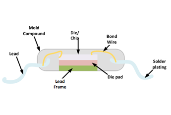
Redistribution Layers (RDLs): This is a foundational technology in FO-PLP that enables rerouting of I/O pads to a more optimal location on the chip’s surface for better interconnection with other components.
Advanced Molding Compounds: Utilized to encapsulate and protect delicate ICs, these materials have been engineered to meet the thermal and mechanical demands of panel-level processing.
Electroless and Electrolytic Plating: These processes are used to form conductive paths on RDLs, crucial for creating high-density interconnects on larger substrates.
Lithography Systems: Adapted for large panel formats, they ensure precise patterning required for circuit miniaturization.
Fan-Out Wafer Level Packaging (FO-WLP)
Predating FO-PLP is Fan-Out Wafer Level Packaging (FO-WLP), a technology that enhanced classic Wafer Level Packaging (WLP) by offering a route to an increased number of I/Os without scaling the die size. FO-WLP employs a “reconstituted wafer” made of individual dies surrounded by a mold compound, which provides the necessary room to redistribute I/Os.
Significant attributes of FO-WLP include:
Chip-First Approach: Dies are placed face-down allowing direct access to the active area for interconnects.
No Requirement for Substrates: The process eliminates the need for a carrier, thereby reducing material costs and package thickness.
Transitioning from FO-WLP to FO-PLP entails a progression to larger panel sizes, potentially leading to cost reductions and enhanced productivity due to the number of units processed concurrently.
Challenges and Solutions in FO-PLP
Despite the promising features of FO-PLP, the transition from wafer to panel-level processing presents several challenges:
Warpage Control: Larger panel sizes can lead to increased warpage, affecting lithography and layer alignment. Utilization of rigid carriers and advanced materials helps mitigate this issue.
Die Placement Accuracy: High precision in die placement is essential, as misalignment can lead to defective packages.
Inspection and Metrology: The larger area increases complexity and time for quality checks.
Addressing these has involved the following solutions:
Advanced Equipment and Automation: Developing robust handling systems and leveraging automation is key in maintaining precision and throughput.
Process Optimization: Refined RDL techniques enhance interconnect resolution, supporting finer pitches and dense packaging configurations.
Collaborative Standards: Industry collaboration on guidelines and specifications ensures consistency and quality across the FO-PLP process.
FO-PLP is poised to revolutionize semiconductor packaging, pivoting on the successful navigation of operational challenges through concerted technological innovation and process development. As it moves into higher scales of production, solving its intrinsic challenges is paramount to its widespread adoption as a staple in advanced microelectronics.
Applications of FO-PLP
Fan-Out Panel-Level Packaging (FO-PLP) is a transformative technology fostering new potentials in several market segments. Its ability to enhance performance, cost efficiency, and interconnect density has made it particularly beneficial in areas demanding high reliability and miniaturization. Here’s how FO-PLP finds application across diverse domains:
Semiconductor Industry
In the semiconductor industry, FO-PLP opens the door for heterogeneous integration, allowing the combination of different semiconductor technologies within a single package. This convergence enables more complex and powerful system-on-chip (SoC) solutions where performance and form factor are critical. Moreover, the increased I/O capabilities resulting from FO-PLP contribute to advancing Moore’s Law, now in terms of packaging innovation rather than just transistor shrinkage.
Advanced Packaging Solutions
With the ever-evolving demands for miniaturization and functionality, FO-PLP stands as an advanced packaging solution that addresses these needs. It fosters the development of 3D packaging solutions by enabling stacking and integration of various dies, which is particularly advantageous for applications like memory and logic chips that require high bandwidth connections. In addition, this technology can aid in the reduction of signal losses and power consumption – key considerations for next-generation electronic devices.
Benefits of FO-PLP in Packaging Solutions:
- Enhanced package density
- Reduced power consumption
- Improved electrical performance
Defense and Aerospace
Reliability and durability are paramount in the defense and aerospace sectors. FO-PLP delivers robustness in packaged components by providing better protection against harsh environments and mechanical stresses. The technology allows for the creation of compact and lightweight electronics that are essential in space-constrained aerospace applications, where every gram counts. Furthermore, improved thermal management attributes of advanced molding compounds in FO-PLP make it suitable for the high-reliability requirements of these fields.
Telecommunications and Networking
The explosion of data in telecommunications networks has called for higher performing chips capable of managing increased bandwidth demands. FO-PLP aids in enabling higher-speed signal transmission while reducing signal loss, making it a favorable choice for networking hardware. In 5G and beyond, where latency and speed are critical, the role of FO-PLP in packaging Radio Frequency (RF) and high-frequency components is significant, contributing directly to the enhancement of wireless communication systems.
Impact on Telecommunications:
- Enabling high-frequency components for 5G
- Reduction of signal loss
- Support for large-scale data throughput
By integrating these capabilities, FO-PLP is undoubtedly setting the pace for emerging technological demands across various high-stakes sectors, securing its position as a key participant in the evolution of electronic packaging.
Future Developments in FO-PLP
Fan-Out Panel-Level Packaging (FO-PLP) stands at the forefront of semiconductor innovation, poised to chart a transformative future for electronic devices. As market forces drive the demand for ever-smaller, more powerful devices, FO-PLP is expected to undergo significant advances. Anticipated future developments aim to push the boundaries of integration, with ongoing research into novel materials, design methodologies, and process technologies. These strides will further amplify FO-PLP’s role in realizing the full potential of heterogeneous integration, shrinking package footprints, and bolstering the overall performance of semiconductor devices.
Advanced Package Miniaturization
The trajectory of FO-PLP is inextricably linked with the relentless trend toward package miniaturization. Intensive R&D endeavors are focusing on scaling the packaging process to accommodate the mounting demand for compact, yet powerful chips. Key to this evolution is the refinement of the Redistribution Layer (RDL), which will enable even finer lines and spaces, enhancing the density of interconnections within the chip package.
Envisioned Milestones for Miniaturization:
- Thinner Redistribution Layers
- Reduced bump pitch
- Smaller die sizes viable for integration
As these technological breakthroughs materialize, FO-PLP will facilitate higher integration levels without sacrificing performance, empowering a new generation of tiny but mighty electronic devices.
Enhancements in Performance and Power Management
Performance and power management stand as twin pillars critical to the advancement of FO-PLP. The evolution of this technology will concentrate on potential performance boosts, alongside methods to curtail power usage. Innovations such as improved thermal interface materials and advanced molding compounds will enhance the dissipation of heat, thereby sustaining high-performance levels in a densely packed package. Meanwhile, advancements in the electrical properties of packaging materials promise to reduce power consumption by minimizing resistive and capacitative losses.
Performance and Power Management Improvements:
- High-efficiency thermal interface materials
- Enhanced electrical properties of packaging substrates
- Integration of power management circuits directly within the package
The synergy of performance and energy efficiency will be crucial in serving energy-sensitive applications such as mobile and wearable technology.
Packaging Technologies for 3D Integration
3D integration represents the next frontier for FO-PLP, where it will play a pivotal role in advancing the vertical stacking of dies. This approach is central to achieving high-density packaging solutions that overcome the real estate limitations of conventional chip designs. Future FO-PLP developments will focus on techniques that allow for finer pitch interconnects, enabling more layers to be stacked with precision, while also ensuring signal integrity and mechanical stability.
Key Areas for 3D Integration Focus:
- Through-package vias for vertical interconnects
- Advanced adhesives for die stacking
- Stress management for stacked dies
As the industry gravitates towards these advanced packaging structures, FO-PLP will serve as a foundational technology platform, seamlessly integrating multiple functional blocks into singular, high-performance components, thus setting new benchmarks in the realm of semiconductor engineering. With each stride in FO-PLP’s evolution, the semiconductor industry is primed for a future of unparalleled integration and innovation.