CST Lab Micro Strip Line
CST Lab Micro Strip Line
Uploaded by
dmpmppCopyright:
Available Formats
CST Lab Micro Strip Line
CST Lab Micro Strip Line
Uploaded by
dmpmppCopyright
Available Formats
Share this document
Did you find this document useful?
Is this content inappropriate?
Copyright:
Available Formats
CST Lab Micro Strip Line
CST Lab Micro Strip Line
Uploaded by
dmpmppCopyright:
Available Formats
ELE3310 Basic Electromagnetics Lab Session 1
Gao Xin By modifying CST MICROWAVE STUDIO 2006 tutorials
Geometric Construction and Solver Settings Introduction and Model Dimensions
In this tutorial you will learn how to simulate planar devices. As a typical example for a planar device, you will analyze a Microstrip Line. The following explanations on how to model and analyze this device can be applied to other planar devices, as well. CST MICROWAVE STUDIO can provide a wide variety of results. This tutorial, however, concentrates solely on the surface currents.
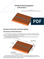
The structure depicted above consists of two different materials: The aluminum oxide substrate (Al2O3) and the stripline metallization. There is no need to model the ground plane since it can easily be described using a perfect electric boundary condition.
Geometric Construction Steps
The tutorial will take you step by step through the construction of your model, and relevant screen shots will be provided so that you can double-check your entries along the way. Select a Template Once you have started CST DESIGN ENVIRONMENT and have chosen to create a new CST MICROWAVE STUDIO project, you are requested to select a template that best fits your current device. Here, the Planar Filter template should be selected.
This template automatically sets the units to mm and GHz, the background material to vacuum and all boundaries to perfect electrical conductors. Because the background material has been set to vacuum, the structure can be modeled just as it appears. Furthermore, the automatic mesh strategy is optimized for planar structures and the solver settings are adjusted to resonant behavior. Set the Units As mentioned, the template has automatically set the geometrical units to mm. However, since all geometrical dimensions are given in mil for this example, you should change this setting manually. Therefore, open the units dialog box by selecting Solve -> Units from the main menu:
Draw the Substrate Brick The first construction step for modeling a planar structure is usually to define the substrate layer. This can be easily achieved by creating a brick made of the substrates material. Please activate the brick creation mode (Objects -> Basic Shapes -> Brick, ). When you are prompted to define the first point, you can enter the coordinates numerically by pressing the Tab key that will open the following dialog box:
In this example, you should enter a substrate block that has an extension of 300 mil in each of the transversal directions. The transversal coordinates can thus be described by X = -150, Y = -150 for the first corner and X = 150, Y = 150 for the opposite corner, assuming that the brick is modeled symmetrically to the origin. Please enter the first points coordinates X = -150 and Y = -150 in the dialog box and press the OK button. You can repeat these steps for the second point: 1 Press the Tab key 2 Enter X = 150, Y = 150 in the dialog box and press OK. Now you will be requested to enter the height of the brick. This can also be numerically specified by pressing the Tab key again, entering the Height of 25 and pressing the OK button. Now the following dialog box will appear showing you a summary of your previous input:
Please check all these settings carefully. If you encounter any mistake, please change the value in the corresponding entry field.
You should now assign a meaningful name to the brick by entering e.g. substrate in the Name field. Since the brick is the first object you have modeled thus far, you can keep the default settings for the first Component (component1). Please note: The use of different components allows you to combine several solids into specific groups, independent of their material behavior. The Material setting of the brick must be changed to the desired substrate material. Because no material has yet been defined for the substrate, you should open the layer definition dialog box by selecting [New Material] from the Material dropdown list:
In this dialog box you should define a new Material name (e.g. Al2O3) and set the Type to a Normal dielectric material. Afterwards, specify the material properties in the Epsilon and Mue fields. Here, you only need to change the dielectric constant Epsilon to 9.9. Finally, choose a color for the material by pressing the Change button. Your dialog box should now look similar to the picture above before you press the OK button. Please note: The defined material Al2O3 will now be available inside the current project for the creation of other solids. However, if you also want to save this specific material definition for other projects, you may check the button Add to material library. You will have access to this material database by clicking on Load from Material Library in the Materials context menu in the navigation tree. Back in the brick creation dialog box you can also press the OK button to finally create the substrate brick. Your screen should now look as follows (you can press the Space key in order to zoom the structure to the maximum possible extent):
Model the Stripline Metallization The next step is to model the stripline metallization on top of the substrate. This can also be easily achieved by creating a brick made of the PEC material. Please check all the settings carefully as shown below before click OK button.
Define Port 1 The next step is to add the ports to the microstrip device. Each port will simulate an infinitely long waveguide (here stripline) structure that is connected to the structure at the ports plane. Waveguide ports are the most accurate way to calculate the microstrip devices and should thus be used here. A waveguide port extends the structure to infinity. Its transversal extension must be large enough to sufficiently cover the microstrip mode. On the other hand, it should not be chosen excessively large in order to avoid higher order mode propagation in the port. A good choice for the width of the port is roughly ten times the width of the stripline. A proper height is about five times the height of the substrate. Applying these guidelines to the example here, you find that the optimum ports width is roughly 250 mil and that its height should be about 125 mil. In this example, the whole model has a width of 300 mil and a height of 150 mil. Because these dimensions are close to the optimal port size you can simply take these dimensions and apply the port to the full extension of the model. Please open the waveguide port dialog box (Solve -> Waveguide Ports, ) to define the first port:
Here, you should set the Normal of the ports plane to the Y-direction and its Orientation in the positive Y-direction (Positive). Because the port should extend across the entire boundary of the model, you can simply keep the Full plane setting for the transversal position. Without the Free normal position check button activated, the port will be allocated as default on the boundary of the calculation domain. The next step is to choose how many modes should be considered by the port. For microstrip devices, a single mode usually propagates along the line. Therefore, you should keep the default setting of one mode. Please finally check the settings in the dialog box and press the OK button to create the port: You can now repeat the same steps for the definition of the opposite port 2: 1 2 3 4 Open the waveguide port dialog box. (Solve -> Waveguide Ports, Set the Normal to Y. Set the Orientation to Negative. Press OK to store the ports settings.
Your model should now look as follows:
Define the Boundary Conditions In this case, the structure is not embedded within a perfect electrically conducting enclosure, Therefore you need to change the boundary conditions to Open for all six boundaries by clicking Solve > Boundary Conditions. Define the Frequency Range The frequency range for the simulation should be chosen with care. The performance of a transient solver can be degraded if the chosen frequency range is too small. We recommend using reasonably large bandwidths of 20% to 100% for the transient simulation. In this example, the frequency range is between 6 and 17 GHz. With the center frequency being 11.5 GHz, the bandwidth (17 GHz 6 GHz = 11 GHz) is about 96% of the center frequency, which is sufficiently large. Thus, you can simply choose the frequency range as desired between 6 and 17 GHz. Please note: Assuming that you were interested primarily in a frequency range of e.g. 11.5 to 12.5 GHz (for a narrow band filter), then the bandwidth would only be about 8.3%. In this case, it would make sense to increase the frequency range (without losing accuracy) to a bandwidth of 30% that corresponds to a frequency range of 10.2 13.8 GHz. This extension of the frequency range could speed up your simulation by more than a factor of three! Also the lower frequency can be set to zero without any problems! The calculation time can often be reduced by half if the lower frequency is set to zero rather than e.g. to 0.01 GHz. After the proper frequency band for this device has been chosen, you can simply open the frequency range dialog box (Solve -> Frequency, ) and enter the range from 6 to 17 (GHz) before pressing the OK button (the frequency unit has previously been set to GHz and is displayed in the status bar):
Define Monitors for the Surface Current
One interesting result for microstrip devices is the current distribution as a function of frequency. The transient solver in CST MICROWAVE STUDIO is able to obtain the surface current distribution for an arbitrary number of frequency samples from a single calculation run. You can define field monitors to specify the frequencies at which the field data shall be stored. Please open the monitor definition dialog box by selecting Solve -> Field Monitors ( ):
In this dialog box you should select the Type H-Field/Surface current before you specify the frequency for this monitor in the Frequency field. Afterwards, you should press the Apply button to store the monitors data. Please define monitors for the following frequencies: 6, 9, 12, 15 (with GHz being the currently active frequency unit). Please make sure that you press the Apply button for each monitor. The monitor definition is then added in the Monitors folder in the navigation tree. The volume in which the fields are recorded is indicated by a box. After the monitor definition is complete, you can close this dialog box by pressing the OK button.
Field Calculation
A key feature of CST MICROWAVE STUDIO is the Method on Demand approach that allows a simulator or mesh type that is best suited for a particular problem. In this case, we choose the transient simulation with a hexahedral mesh.
Transient Solver
Transient Solver Settings The transient solver parameters are specified in the solver control dialog box that can be opened by selecting Solve -> Transient Solver from the main menu or by pressing the Transient solver icon in the toolbar.
Because the structure is fully symmetric, so change the Source type to Port 1. Finally, press the Start button to start the calculation. A progress bar and abort button appear in the status bar, displaying some information about the solver stages.
During the simulation, the Message Window will show some details about the performed simulation. Congratulations, you have simulated the microstrip lineusing the transient solver! Lets review the results. 2D and 3D Results (Port Modes and Field Monitors) Finally, you can observe the 2D and 3D field results. You should first inspect the port modes that can be easily displayed by opening the 2D/3D Results -> Port Modes -> Port1 folder of the navigation tree. To visualize the electric field of the fundamental port mode you should click on the e1 folder. After properly rotating the view and tuning some settings in the plot properties dialog box, you should obtain a plot similar to the following picture.
The plot also shows some important properties of the mode such as mode type, propagation constant and line impedance. The port mode at the second port can be visualized in the same manner. The three-dimensional surface current distribution on the conductors can be shown by selecting one of the entries in the 2D/3D Results -> Surface Current folder in the navigation tree. The surface current at a frequency of 15 GHz can thus be visualized by clicking at the 2D/3D Results -> Surface Current -> h-field (f=15) [1] entry:
You can toggle an animation of the currents on and off by selecting Results -> Animate Fields. The surface currents for the other frequencies can be visualized in the same manner.
You might also like
- Digital Spectral Analysis MATLAB® Software User GuideFrom EverandDigital Spectral Analysis MATLAB® Software User GuideNo ratings yet
- Optimum Array Processing: Part IV of Detection, Estimation, and Modulation TheoryFrom EverandOptimum Array Processing: Part IV of Detection, Estimation, and Modulation TheoryNo ratings yet
- CST Microwave Studio: General Purpose Solver 3d-VolumeNo ratings yetCST Microwave Studio: General Purpose Solver 3d-Volume30 pages
- 4 1 2 Uwb Antenne Simulation With CST Microwave Studio100% (1)4 1 2 Uwb Antenne Simulation With CST Microwave Studio24 pages
- Printed Dipole Antenna With Integrated BalunNo ratings yetPrinted Dipole Antenna With Integrated Balun3 pages
- Boundary and Excitation Training: February 2003No ratings yetBoundary and Excitation Training: February 200330 pages
- CST STUDIO SUITE - High Frequency Simulation100% (1)CST STUDIO SUITE - High Frequency Simulation128 pages
- Low Frequency Electro Magnetic Design and Simulation: CST em StudioNo ratings yetLow Frequency Electro Magnetic Design and Simulation: CST em Studio2 pages
- Fundamentals of Microwave Communication PDFNo ratings yetFundamentals of Microwave Communication PDF51 pages
- 3 - Two Methods For The Measurement of Substrate Dielectric Constant-Das-D PozarNo ratings yet3 - Two Methods For The Measurement of Substrate Dielectric Constant-Das-D Pozar7 pages
- Co-Planar Waveguide (Driven Terminal) : GroundNo ratings yetCo-Planar Waveguide (Driven Terminal) : Ground6 pages
- Optical and Microwave Technologies for Telecommunication NetworksFrom EverandOptical and Microwave Technologies for Telecommunication NetworksNo ratings yet
- RF Analog Impairments Modeling for Communication Systems Simulation: Application to OFDM-based TransceiversFrom EverandRF Analog Impairments Modeling for Communication Systems Simulation: Application to OFDM-based TransceiversNo ratings yet
- Modeling of Digital Communication Systems Using SIMULINKFrom EverandModeling of Digital Communication Systems Using SIMULINKNo ratings yet
- Introduction to Optical Waveguide Analysis: Solving Maxwell's Equation and the Schrödinger EquationFrom EverandIntroduction to Optical Waveguide Analysis: Solving Maxwell's Equation and the Schrödinger EquationNo ratings yet
- Signal Integrity: From High-Speed to Radiofrequency ApplicationsFrom EverandSignal Integrity: From High-Speed to Radiofrequency ApplicationsNo ratings yet
- Microwave Filters for Communication Systems: Fundamentals, Design, and ApplicationsFrom EverandMicrowave Filters for Communication Systems: Fundamentals, Design, and ApplicationsNo ratings yet
- Master of Information & Communication Technology Management (Mictm)No ratings yetMaster of Information & Communication Technology Management (Mictm)2 pages
- Research Article: Clinical Profile and Visual Outcome of Ocular Bartonellosis in MalaysiaNo ratings yetResearch Article: Clinical Profile and Visual Outcome of Ocular Bartonellosis in Malaysia7 pages
- Master of Science (Management) : Asia UniversityNo ratings yetMaster of Science (Management) : Asia University2 pages
- Case Report: Giant Preputial Calculus: The First Reported Case in MalaysiaNo ratings yetCase Report: Giant Preputial Calculus: The First Reported Case in Malaysia4 pages
- Master in Management (MIM) : Asia UniversityNo ratings yetMaster in Management (MIM) : Asia University2 pages
- Master of Human Resource Management (MHRM) : Asia UniversityNo ratings yetMaster of Human Resource Management (MHRM) : Asia University2 pages
- Master of Education (Med) : Asia UniversityNo ratings yetMaster of Education (Med) : Asia University2 pages
- Terms and Conditions of Financial Incentives: DiscountNo ratings yetTerms and Conditions of Financial Incentives: Discount3 pages
- PHD (Business Administration) : Asia UniversityNo ratings yetPHD (Business Administration) : Asia University2 pages
- Sheikh Yusuf Al-Qaradawi A Moderate Voice From TheNo ratings yetSheikh Yusuf Al-Qaradawi A Moderate Voice From The14 pages
- PHD (Social & Behavioral Science) : Asia UniversityNo ratings yetPHD (Social & Behavioral Science) : Asia University2 pages
- School of Education & Cognitive Science Master of Education: Learning ObjectivesNo ratings yetSchool of Education & Cognitive Science Master of Education: Learning Objectives2 pages
- RM 438 RM 360: (Departing Flight Must Arrange After 18:00 PM)No ratings yetRM 438 RM 360: (Departing Flight Must Arrange After 18:00 PM)1 page
- Imposition of The Death Penalty Upon The Poor, Racial Minorities, The Intellectually Disabled and The Mentally IllNo ratings yetImposition of The Death Penalty Upon The Poor, Racial Minorities, The Intellectually Disabled and The Mentally Ill18 pages
- The Even - and Odd-Mode Capacitance Parameters For Coupled Lines in Suspended SubstrateNo ratings yetThe Even - and Odd-Mode Capacitance Parameters For Coupled Lines in Suspended Substrate8 pages
- 3.5 GHZ Microstrip Transmission Line Design For Microwave IC'sNo ratings yet3.5 GHZ Microstrip Transmission Line Design For Microwave IC's4 pages
- Dipoles: Wideband Dipole Antenna For BaseNo ratings yetDipoles: Wideband Dipole Antenna For Base4 pages
- Chapter 3 Transmission Line and Waveguide: Field Solution Field Solution (Cont'd)No ratings yetChapter 3 Transmission Line and Waveguide: Field Solution Field Solution (Cont'd)14 pages
- (IEE ELECTROMAGNETIC WAVES SERIES 12) David M. Pozar, Daniel H. Schaubert - Microstrip Antennas - The Analysis and Design of Microstrip Antennas and Arrays (1995, Wiley-IEEE Press) PDFNo ratings yet(IEE ELECTROMAGNETIC WAVES SERIES 12) David M. Pozar, Daniel H. Schaubert - Microstrip Antennas - The Analysis and Design of Microstrip Antennas and Arrays (1995, Wiley-IEEE Press) PDF306 pages
- Comparing Microstrip and CPW PerformanceNo ratings yetComparing Microstrip and CPW Performance6 pages
- Dual Directional Coupler Design Duroid 5880No ratings yetDual Directional Coupler Design Duroid 58805 pages
- Understanding PCBs For High-Frequency ApplicationsNo ratings yetUnderstanding PCBs For High-Frequency Applications4 pages
- All About Trnasmission Lines and Waveguides PDFNo ratings yetAll About Trnasmission Lines and Waveguides PDF19 pages
- (MWJ0210) Reviewing The Basics of Suspended StriplinesNo ratings yet(MWJ0210) Reviewing The Basics of Suspended Striplines5 pages
- Broadside-Coupled Coplanar Waveguides and Their End-Coupled Band-Pass Filter ApplicationsNo ratings yetBroadside-Coupled Coplanar Waveguides and Their End-Coupled Band-Pass Filter Applications9 pages
- A Comprehensive Comparison of Stripline vs. MicrostripNo ratings yetA Comprehensive Comparison of Stripline vs. Microstrip10 pages
- Analysis of Stripline-Fed Slot-Coupled Patch Antennas With Vias For Parallel-Plate Mode SuppressionNo ratings yetAnalysis of Stripline-Fed Slot-Coupled Patch Antennas With Vias For Parallel-Plate Mode Suppression8 pages
- 529 - Microwave Circuit Design by PrashanthNo ratings yet529 - Microwave Circuit Design by Prashanth38 pages
- Digital Spectral Analysis MATLAB® Software User GuideFrom EverandDigital Spectral Analysis MATLAB® Software User Guide
- Optimum Array Processing: Part IV of Detection, Estimation, and Modulation TheoryFrom EverandOptimum Array Processing: Part IV of Detection, Estimation, and Modulation Theory
- CST Microwave Studio: General Purpose Solver 3d-VolumeCST Microwave Studio: General Purpose Solver 3d-Volume
- 4 1 2 Uwb Antenne Simulation With CST Microwave Studio4 1 2 Uwb Antenne Simulation With CST Microwave Studio
- Low Frequency Electro Magnetic Design and Simulation: CST em StudioLow Frequency Electro Magnetic Design and Simulation: CST em Studio
- 3 - Two Methods For The Measurement of Substrate Dielectric Constant-Das-D Pozar3 - Two Methods For The Measurement of Substrate Dielectric Constant-Das-D Pozar
- Optical and Microwave Technologies for Telecommunication NetworksFrom EverandOptical and Microwave Technologies for Telecommunication Networks
- RF Analog Impairments Modeling for Communication Systems Simulation: Application to OFDM-based TransceiversFrom EverandRF Analog Impairments Modeling for Communication Systems Simulation: Application to OFDM-based Transceivers
- Smart Antennas: Recent Trends in Design and ApplicationsFrom EverandSmart Antennas: Recent Trends in Design and Applications
- Modeling of Digital Communication Systems Using SIMULINKFrom EverandModeling of Digital Communication Systems Using SIMULINK
- Introduction to Optical Waveguide Analysis: Solving Maxwell's Equation and the Schrödinger EquationFrom EverandIntroduction to Optical Waveguide Analysis: Solving Maxwell's Equation and the Schrödinger Equation
- Signal Integrity: From High-Speed to Radiofrequency ApplicationsFrom EverandSignal Integrity: From High-Speed to Radiofrequency Applications
- OFDM-Based Broadband Wireless Networks: Design and OptimizationFrom EverandOFDM-Based Broadband Wireless Networks: Design and Optimization
- Fundamentals of RF and Microwave Transistor AmplifiersFrom EverandFundamentals of RF and Microwave Transistor Amplifiers
- Design of Integrated Circuits for Optical CommunicationsFrom EverandDesign of Integrated Circuits for Optical Communications
- Microwave Filters for Communication Systems: Fundamentals, Design, and ApplicationsFrom EverandMicrowave Filters for Communication Systems: Fundamentals, Design, and Applications
- Radio Propagation Measurement and Channel ModellingFrom EverandRadio Propagation Measurement and Channel Modelling
- Master of Information & Communication Technology Management (Mictm)Master of Information & Communication Technology Management (Mictm)
- Research Article: Clinical Profile and Visual Outcome of Ocular Bartonellosis in MalaysiaResearch Article: Clinical Profile and Visual Outcome of Ocular Bartonellosis in Malaysia
- Case Report: Giant Preputial Calculus: The First Reported Case in MalaysiaCase Report: Giant Preputial Calculus: The First Reported Case in Malaysia
- Master of Human Resource Management (MHRM) : Asia UniversityMaster of Human Resource Management (MHRM) : Asia University
- Terms and Conditions of Financial Incentives: DiscountTerms and Conditions of Financial Incentives: Discount
- Sheikh Yusuf Al-Qaradawi A Moderate Voice From TheSheikh Yusuf Al-Qaradawi A Moderate Voice From The
- PHD (Social & Behavioral Science) : Asia UniversityPHD (Social & Behavioral Science) : Asia University
- School of Education & Cognitive Science Master of Education: Learning ObjectivesSchool of Education & Cognitive Science Master of Education: Learning Objectives
- RM 438 RM 360: (Departing Flight Must Arrange After 18:00 PM)RM 438 RM 360: (Departing Flight Must Arrange After 18:00 PM)
- Imposition of The Death Penalty Upon The Poor, Racial Minorities, The Intellectually Disabled and The Mentally IllImposition of The Death Penalty Upon The Poor, Racial Minorities, The Intellectually Disabled and The Mentally Ill
- The Even - and Odd-Mode Capacitance Parameters For Coupled Lines in Suspended SubstrateThe Even - and Odd-Mode Capacitance Parameters For Coupled Lines in Suspended Substrate
- 3.5 GHZ Microstrip Transmission Line Design For Microwave IC's3.5 GHZ Microstrip Transmission Line Design For Microwave IC's
- Chapter 3 Transmission Line and Waveguide: Field Solution Field Solution (Cont'd)Chapter 3 Transmission Line and Waveguide: Field Solution Field Solution (Cont'd)
- (IEE ELECTROMAGNETIC WAVES SERIES 12) David M. Pozar, Daniel H. Schaubert - Microstrip Antennas - The Analysis and Design of Microstrip Antennas and Arrays (1995, Wiley-IEEE Press) PDF(IEE ELECTROMAGNETIC WAVES SERIES 12) David M. Pozar, Daniel H. Schaubert - Microstrip Antennas - The Analysis and Design of Microstrip Antennas and Arrays (1995, Wiley-IEEE Press) PDF
- Understanding PCBs For High-Frequency ApplicationsUnderstanding PCBs For High-Frequency Applications
- (MWJ0210) Reviewing The Basics of Suspended Striplines(MWJ0210) Reviewing The Basics of Suspended Striplines
- Broadside-Coupled Coplanar Waveguides and Their End-Coupled Band-Pass Filter ApplicationsBroadside-Coupled Coplanar Waveguides and Their End-Coupled Band-Pass Filter Applications
- A Comprehensive Comparison of Stripline vs. MicrostripA Comprehensive Comparison of Stripline vs. Microstrip
- Analysis of Stripline-Fed Slot-Coupled Patch Antennas With Vias For Parallel-Plate Mode SuppressionAnalysis of Stripline-Fed Slot-Coupled Patch Antennas With Vias For Parallel-Plate Mode Suppression


