IEEE TRANSACTIONS ON COMPONENTS AND PACKAGING TECHNOLOGIES, VOL. 24, NO. 1, MARCH 2001
33
A Voltage-Controlled Tunable Thin-Film Distributed
RC Notch Filter
Won-Youl Choi and Susan Trolier-McKinstry, Member, IEEE
Abstract—Notch filters are widely used in communication
and instrumentation systems not only for eliminating undesired
frequencies and for measuring transient harmonic distortions, but
also as central components of selective filters and oscillators in
feedback arrangements. This paper describes the characteristics
of a thin-film distributed RC (DRC) notch filter made from
Au/TaN/Y-doped BaTiO3 (Y-BT)/Pt. The dielectric (Y-BT) and
resistive (TaN) films were grown by pulsed laser deposition (PLD).
A notch frequency of 2.8 MHz and notch depth of 76.7 dB were
measured from zero with a notch resistance (
) of 34 . The
experimental optimum notch parameters of
were obtained. Tunability of the notch
and
frequency was observed with an applied dc bias voltage.
=
= 33 0
=
= 19 7
Index Terms—BaTiO3 thin film, pulsed laser deposition, RC
notch filter, TaN thin film, Y-doping.
I. INTRODUCTION
T
HE USE of distributed-RC (DRC) rather than lumped-RC
(LRC) networks as frequency-selective elements in hybrid
integrated-circuit active filters has been advocated as offering
the practical advantages of increased simplicity and reliability
[1]. For example, Kaufman [2] and Kaufman and Garrett [3]
studied a notch filter consisting of an RC transmission line
fabricated on a semiconductor substrate in conjunction with a
lumped resistance and described the effect of geometrical tapering on the characteristics of DRC substrates. Su [4] reported
an RC filter with staggered notch frequencies fabricated using
Teledetos paper and Myler film as the resistive and dielectric
films, respectively. Ahmad and Singh [5] fabricated a thin film
uniformly DRC structure consisting of Al/Al O –SiO/Ni–Cr
films using vacuum evaporation. The electrical performance of
uniformly DRC notch networks fabricated using conventional
integrated circuit (IC) thin-film vacuum deposition techniques
and a very large scale integration (VLSI) interlevel silicon
dioxide spin-on glass (SOG) dielectric planarization material
was reported by Kolesar [6].
For such a filter, the optimum null in the open-circuit
voltage-transfer function is obtained for a particular ratio of
the resistors, and the frequency of the null is then determined
by the RC product. Hence, if the capacitance of the distributed
section couldbechangedwithoutchangingtheresistance,anideal
Manuscript received July 25, 2000; revised November 3, 2000. This work
was supported by the TDK Cooperation. This paper was recommended for publication by Associate Editor A. Deutsch upon evaluation of the reviewers’ comments.
W.-Y. Choi is with the MEMS Laboratory, S&C Sector, Samsung Advanced
Institute of Technology, Suwon 440–600, Korea.
S. Trolier-McKinstry is with the Materials Research Laboratory, Pennsylvania State University, University Park, PA 16802 USA.
Publisher Item Identifier S 1521-3331(01)01381-2.
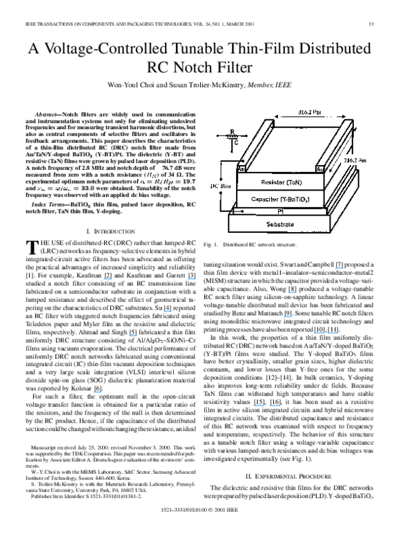
Fig. 1.
Distributed RC network structure.
tuning situation would exist. Swart and Campbell [7] proposed a
thin film device with metal1–insulator–semiconductor–metal2
(MISM) structure in which the capacitor provided a voltage-variable capacitance. Also, Wong [8] produced a voltage-tunable
RC notch filter using silicon-on-sapphire technology. A linear
voltage-tunable distributed null device has been fabricated and
studied by Benz and Mattauch [9]. Some tunable RC notch filters
using monolithic microwave integrated circuit technology and
printing processes have also been reported [10], [11].
In this work, the properties of a thin film uniformly distributed RC (DRC) network based on Au/TaN/Y-doped BaTiO
(Y-BT)/Pt films were studied. The Y-doped BaTiO films
have better crystallinity, smaller grain sizes, higher dielectric
constants, and lower losses than Y-free ones for the some
deposition conditions [12]–[14]. In bulk ceramics, Y-doping
also improves long-term reliability under dc fields. Because
TaN films can withstand high temperatures and have stable
resistivity values [15], [16], it has been used as a resistive
film in active silicon integrated circuits and hybrid microwave
integrated circuits. The distributed capacitance and resistance
of this RC network was examined with respect to frequency
and temperature, respectively. The behavior of this structure
as a tunable notch filter using a voltage-variable capacitance
with various lumped-notch resistances and dc bias voltages was
investigated experimentally (see Fig. 1).
II. EXPERIMENTAL PROCEDURE
The dielectric and resistive thin films for the DRC networks
werepreparedbypulsedlaserdeposition(PLD).Y-dopedBaTiO
1521–3331/01$10.00 © 2001 IEEE
�34
IEEE TRANSACTIONS ON COMPONENTS AND PACKAGING TECHNOLOGIES, VOL. 24, NO. 1, MARCH 2001
TABLE I
PULSED LASER DEPOSITION PARAMETERS FOR DIELECTRIC (Y-BT) AND RESISTIVE (TaN) FILM GROWTH
Fig. 2. Dielectric constants and dissipation factors (tan� ) of the dielectric
(Y-BT) film as a function of frequency.
(Y-BT) and TaN film were used as the dielectric and resistive
films, respectively. The specific deposition parameters are given
in Table I. Y-BT and TaN films were grown in pure (99.99%)
N atmospheres from 0.2wt% Y O doped BaTiO ceramic
and a 99.95% pure Ta metal target, respectively. Pt/Ti/SiO /Si
substrates were used. In both cases, a
Hz pulsed laser
J/cm ,
repetition frequency with an energy density of
and a working pressure of 100 mtorr were found to yield good
film properties. Growth temperatures spanning 300 C to 700 C
were achieved by adhering the substrates to a stainless steel
block-style heater with silver paint. The growth temperature for
the TaN film was deliberately kept low to minimize reaction with
the underlying capacitor film. A Lambda Physik Compex 102
excimer laser operating at 248 nm was used. The top electrode
(Au)filmwasdepositedatroomtemperature bydcsputtering.Top
Å thickness were fabricated by
electrode patterns with a
photolithography and wet etching processes.
The crystallinity of the Y-BT and TaN films was examined
with an X-ray diffractometer using Cu K radiation (Scintag,
Inc.). The dielectric constants and dissipation factors (tan ) of
the Y-BT films were measured using a HP4194A impedance analyzer with a 0.03 V oscillation level or HP 4284A LCR meter.
The sheet resistance of the TaN films on the SiO /Si substrates
were measured as a function of temperature using a four-point
probe and a Fluke 8840A multimeter. A computer controlled
Fig. 3. Permittivity of the Y-BT dielectric film and sheet resistance of the TaN
resistive film as a function of temperature.
Delta Design oven was used to control the temperature between
100 C and 200 C.
Following the fabrication of the notch filters, the surface and
cross-sectional morphologies of the layers were observed with
optical microscopy and scanning electron microscopy (SEM).
The open-circuit voltage transfer function of the DRC notch
filter was measured using the HP 4194A impedance analyzer.
To satisfy the optimum null condition for the notch filter, a variable resistance lumped-notch resistor was used. Tunability was
) and the dc bias
examined with various notch resistances (
voltages generated by the HP4192A impedance analyzer.
III. RESULTS AND DISCUSSION
anddissipationfactors
Fig.2showsthedielectricconstants
(tan ) of Y-BT films on Pt/Ti/SiO /Si substrates as a function of
frequency.Inordertomeasurethedielectricconstantsanddissipation factors (tan ) of the Y-BT dielectric layers, 0.3 mm diameter
Pt top electrodes were sputtered through a shadow mask onto the
and
top surface of the films. Dielectric constants of
dissipationfactors (tan ) of 0.03 at 1 kHzwere observed. The temperature dependence of the permittivity for Y-BT films as well as
thesheetresistanceofTaNfilms(onSiO /Sisubstrates)areshown
inFig.3.ThedielectricconstantatroomtemperatureandtheCurie
point at 10 kHz are 1150 and 123 C, respectively. The high temperature dielectric data were fitted to the Curie–Weiss model (the
�CHOI AND MCKINSTRY: VOLTAGE-CONTROLLED TUNABLE THIN-FILM DISTRIBUTED RC NOTCH FILTER
Fig. 4.
35
(a) Surface optical microscopy image and (b) cross-sectional SEM images of distributed RC network.
where
linearrelationshipbetweentheinversedielectricconstantandtemperature above the ferroelectric transition) [17]
Curie constant;
absolute temperature;
Curie temperature.
TheCurieconstantwascalculatedfromthehightemperaturedata.
TheCurieconstantisontheorderof10 K .Thesheetresistance
of the TaN film at room temperature (20 C) is 670 , and the temperature coefficient ofresistance (TCR) is 920 ppm/ C.
Fig. 4 shows SEM micrographs of the top surface and
cross-sections of the distributed filter structure obtained by
photolithography and wet etching of the Au top electrode.
Good top electrode patterns for uniformly DRC networks were
obtained. The thicknesses of the dielectric Y-BT film and
Å and
Å, respectively.
resistive TaN film were
From the thicknesses and effective area (316.2 m 316.2 m)
of the dielectric and resistive films, a distributed capacitance of
2.8 nF and resistance of 670 were calculated, assuming no
reaction layers between the films.
It has been shown [18] that the open circuit voltage transfer
function, , of a uniformly DRC notch filter with dielectric dissipation is given by
(1)
(2)
Fig. 5. Measured open-circuit voltage transfer function of the fabricated DRC
network for various notch resistances (R ).
�36
Fig. 6.
IEEE TRANSACTIONS ON COMPONENTS AND PACKAGING TECHNOLOGIES, VOL. 24, NO. 1, MARCH 2001
Notch frequency and depth with notch parameters (
= R=R
).
where
is expressed in terms of a freand a frequency dequency normalization parameter
. In these
pendent normalized dielectric dissipation factor
, where and , respectively, derelationships
note the distributed resistance and capacitance of the structure.
, and the parameter ( ) is given as
in terms of the lumped notch resistance (
). The zero of transmission in (2) that yields the optimum notch condition is realized when both the real and imaginary components of the numerator are zero. In particular, the optimum notch parameters
) and free of
for an ideal notch filter which is a lossless (
and
.
parasitics are
In this work, the experimentally observed open-circuit
voltage transfer function of the fabricated DRC notch filter is
,
shown in Fig. 5 together with its circuit (having
nF, and
kHz). The
values found for the notch frequency and notch depth when
were 2.8 MHz and 76.7 dB, respectively.
This gives the experimental optimum notch parameters
and
. The difference between the values of the notch parameters obtained
experimentally and those predicted theoretically may be due
to the dissipation factor (tan ) of the dielectric film (Y-BT)
and parasitics. In addition, it is possible that a tantalum oxide
(TaO ) with a low dielectric constant was unintentionally
formed between the capacitor and the resistor during the nitride
film growth. Any tantalum oxide phase present would decrease
the total distributed capacitance of the RC network and causes
the optimum notch frequency to shift to higher values.
)
The behavior of the notch filter with notch resistance (
were observed. For
and
, the notch frequencies obtained were 2.90 MHz, 2.88
MHz, 2.83 MHz, 2.82 MHz, 2.80 MHz, and 2.76 MHz, respectively. The variation of the notch frequency and depth with notch
) is plotted in Fig. 6. The relatively high
parameter (
dB may be due to the high resistance TaN
insertion loss of
film. A lower insertion loss could probably be achieved with a
higher conductivity resistive film.
The notch filter could also be tuned with a dc bias voltage, independently of the distributed resistance. This is due to the field
dependence of the dielectric constants of the Y-BT film. Fig. 7
Fig. 7. Measured open-circuit voltage transfer function of the fabricated DRC
network for various dc bias voltages.
Fig. 8.
Dielectric constant of the Y-BT film as a function of dc bias voltage.
Fig. 9. Notch frequency and depth variation with dc bias voltage.
shows the measured open-circuit voltage transfer function of a
DRC network made with a thicker dielectric film (Y-BT) for
various dc bias voltages. Fig. 8 shows the dielectric constant
( ) of a Y-BT film as a function of dc bias voltage. Given the
decrease in the Y-BT film permittivity with field, the distributed
capacitance should drop with increased dc bias voltage, and the
�CHOI AND MCKINSTRY: VOLTAGE-CONTROLLED TUNABLE THIN-FILM DISTRIBUTED RC NOTCH FILTER
notch frequency should shift to higher values. The notch frequency and depth as a function of dc bias voltage are shown
in Fig. 9. The notch depth decreased with increasing dc bias
voltage when the notch resistance was kept constant.
The behavior of this structure as a tunable notch filter using a
voltage-variable capacitance with various lumped-notch resistances and dc bias voltage will be optimized for use in integrated-circuit network applications at radio frequencies.
IV. CONCLUSIONS
Dielectric (Y-BT) and resistive (TaN) films for distributed RC
notch filters were fabricated by pulsed laser deposition (PLD).
The dielectric constant and dissipation factor (tan ) of Y-BT
films at 10 kHz were 1150 and 0.03, respectively. TaN films
had a sheet resistance of 670 at room temperature and a temperature coefficient of resistance (TCR) of 920 ppm/ C.
A notch frequency of 2.8 MHz and depth of 76.7 dB were
) of 34 for a 316.2 m
measured at a notch resistance (
316.2 m distributed filter. Experimental optimum notch parameters of
and
were obtained. Tunability of the notch frequency with dc bias
voltage was also observed. With further optimization of the insertion loss, these characteristics of the thin film DRC notch filters should allow them to be used in integrated-circuit network
applications at radio frequencies.
REFERENCES
[1] L. P. Huelsman, “The distributed-lumped-active network,” IEEE Spectrum, vol. 6, p. 51, Aug. 1969.
[2] W. M. Kaufman, “Theory of monolithic null device and some novel circuit applications,” Proc. IRE, vol. 48, p. 1540, 1960.
[3] W. M. Kaufman and S. J. Garrett, “Tapered distributed filters,” IRE
Trans. Circuit Theory, vol. 9, p. 329, 1962.
[4] K. L. Su, “RC filters with staggered notch frequencies,” Proc. IEEE, vol.
54, p. 1199, Sept. 1966.
[5] S. Ahmad and R. Singh, “A composite dielectric thin film notch filter,”
Thin Solid Films, vol. 67, p. L63, 1980.
[6] E. S. Kolesar, “Effects of thin film spin-on glass dielectric loss on the
performance of the uniformly distributed RC notch network,” IEEE
Trans. Comp., Hybrids, Manufact. Technol., vol. 14, p. 413, June 1991.
[7] P. L. Swart and C. K. Campbell, “A voltage-controlled tunable distributed RC filter,” Solid-State Circuits, vol. SC-7, p. 306, 1972.
[8] P. H. K. Wong and L. Young, “A new voltage-tunable distributed RC
notch filter suitable for SOS realization,” Proc. IEEE, vol. 62, p. 523,
Apr. 1977.
[9] H. F. Benz and R. J. Mattauch, “A linear voltage-tunable distributed null
device,” IEEE J. Solid-State Circuits, vol. SC-7, p. 499, Dec. 1972.
[10] S. Lucyszyn and I. D. Robertson, “MMIC tunable active notch filter,”
Electron. Lett., vol. 32, p. 980, 1996.
[11] P. S. A. Evans, B. J. Ramsey, P. M. Harrey, and D. J. Harrison, “Printed
analogue filter structures,” Electron. Lett., vol. 35, p. 306, 1999.
[12] W. Choi, Y. Tsur, C. A. Randall, and S. Trolier-McKinstry, “Effect of
Y-doping on the dielectric properties of BaTiO films deposited in reducing atmospheres using pulsed laser deposition,” in Proc. MRS, 1999,
to be published.
37
[13] S. Sato, Y. Nakano, A. Sato, and T. Nonura, “Effect of Y-doping on resistance degradation of multilayer ceramic capacitors with Ni electrodes
under the highly accelerated life test,” Jpn. J. Appl. Phys., vol. 36, p.
6016, 1997.
[14] Y. Nakano, A. Sato, A. Hitomi, and T. Nonura, “Microstructure and related phenomena of multilayer ceramic capacitors with Ni-electrode,”
Ceramic Trans., vol. 32, p. 119, 1993.
[15] K. Radhakrishnan, N. Geok Ing, and R. Gopalakrishnan, “Reactive
sputter deposition and characterization of tantalum nitride thin films,”
Mater. Sci. Eng., vol. B57, p. 224, 1999.
[16] C. Au, W. Anderson, D. Schmitz, J. Flassayer, and F. Collins, “Stability
of tantalum nitride thin film resistors,” J. Mater. Res., vol. 5, no. 6, p.
1224, 1990.
[17] B. Jaffe, W. R. Cook Jr., and H. Jaffe, Piezoelectric Ceramics. New
York: Academic, 1971.
[18] J. A. Carson, C. K. Campbell, P. L. Swart, and F. J. Vallo, “Effects of
dielectric losses on the performance of evaporated thin film distributed
RC notch filters,” IEEE J. Solid-State Circuits, vol. SC-6, p. 120, June
1971.
Won-Youl Choi received the B.S. degree from
Hanyang University, Seoul, Korea, and the M.S. and
Ph.D. degrees in materials science and engineering
from the Korean Advanced Institute of Science and
Technology, Taejon.
He was a Postdoctoral Researcher with the
Materials Research Laboratory, Pennsylvania State
University, University Park. In 2000, he joined
the Samsung Advanced Institute of Technology,
Suwon, Korea, as a Special Researcher. His main
research interests include ferroelectric thin films for
dielectric applications, the characterization of the electrical and mechanical
properties of thin films, and micromachining technology for microsensors and
microactuators.
Susan Trolier-McKinstry (M’92) received the M.S.
and Ph.D. degrees in ceramic science from Pennsylvania State University (PSU), University Park.
She is an Associate Professor of Ceramic Science
and Engineering and Associate Director of the Materials Research Laboratory, PSU. Her main research
interests include ferroelectric thin films for actuator
and dielectric applications, the development of texture in bulk ceramic piezoelectrics, and spectroscopic
ellipsometry. She has held visiting appointments at
Hitachi Central Research Laboratory, the Army Research Laboratory, and the Ecole Polytechnique Federale de Lausanne.
Dr. Trolier-McKinstry received the Robert Coble Award of the American Ceramic Society, the Wilson Award for Outstanding Teaching in the College of
Earth and Mineral Sciences, and an NSF CAREER grant. She is a member
of the American Ceramic Society, the Materials Research Society, ASM, and
ASEE. She is co-chair of the committee revising the IEEE Standard on Ferroelectricity. She is an Elected Member of the IEEE Ultrasonics, Ferroelectrics,
and Frequency Control Society Advisory Committee. She is past-President of
Keramos and Treasurer for the Ceramics Education Council.
�
 Susan Trolier-McKinstry