IEEE TRANSACTIONS ON BIOMEDICAL CIRCUITS AND SYSTEMS, VOL. 5, NO. 3, JUNE 2011
231
An Implementation of a Spike-Response Model
With Escape Noise Using an Avalanche Diode
Thomas Clayton, Katherine Cameron, Member, IEEE, Bruce R. Rae, Member, IEEE, Nancy Sabatier,
Edoardo Charbon, Senior Member, IEEE, Robert K. Henderson, Member, IEEE, Gareth Leng, and
Alan Murray, Fellow, IEEE
Abstract—This paper introduces a novel probabilistic spike-response model through the combination of avalanche diode-generated Poisson distributed noise, and a standard exponential
decay-based spike-response curve. The noise source, which is
derived from a 0.35- m single-photon avalanche diode (kept in
the dark), was tested experimentally to verify its characteristics,
before being combined with a field-programmable gate-array
implementation of a spike-response model. This simple model was
then analyzed, and shown to reproduce seven of eight behaviors
recorded during an extensive study of the ventral medial hypothalamic (VMH) region of the brain. It is thought that many of the cell
types found within the VMH are fed from a tonic noise synaptic
input, where the patterns generated are a product of their spike
response and not their interconnection. This paper shows how this
tonic noise source can be modelled, and due to the independent
nature of the noise sources, provides an avenue for the exploration
of networks of noise-fueled neurons, which play a significant role
in pattern generation within the brain.
Index Terms—Modelling, single-photon avalanche
(SPAD), spike-response model, spiking neuron.
diode
I. INTRODUCTION
HIS paper presents the initial proof of concept for a novel
implementation of a probabilistic cumulative spike-response neural model (CSRM) with escape noise through the
use of an avalanching diode acting as a Poisson distributed
noise source. Most integrated-circuit (IC)–based spiking neural
models are deterministic in nature, where incoming synaptic
events are integrated on a capacitive membrane with either a
firing threshold (integrate-and-fire-based models) [1], [2] or
voltage-dependent feedback mechanisms (conductance-based
models) [3]–[5] to determine spike generation. Deterministic
models have been used extensively to investigate single-neuron
T
Manuscript received February 16, 2010; revised May 25, 2010 and September
22, 2010; accepted November 22, 2010. Date of publication January 28, 2011;
date of current version May 25, 2011. The work was supported in part by EPSRC
Grant EP/C516583/1 and in part by the Scottish Funding Council for the Joint
Research Institute with the Heriot-Watt University, which is part of the Edinburgh Research Partnership in Engineering and Mathematics (ERPem). This
paper was recommended by Associate Editor R. Etienne-Cummings.
T. Clayton, K. Cameron, B. R. Rae, R. K. Henderson, and A. Murray are with
the Institute of Integrated Micro and Nano Systems, Joint Research Institute
for Integrated Systems, School of Engineering, University of Edinburgh, Edinburgh, EH9 3JL, U.K. (e-mail: T.Clayton@ed.ac.uk; K.Cameron@ed.ac.uk).
N. Sabatier and G. Leng are with the Centre for Integrative Physiology,
School of Biomedical Sciences, University of Edinburgh, Edinburgh, EH8
9XD, U.K.
E. Charbon is with TU Delft, Delft 2628 CD, The Netherlands.
Color versions of one or more of the figures in this paper are available online
at http://ieeexplore.ieee.org.
Digital Object Identifier 10.1109/TBCAS.2010.2100392
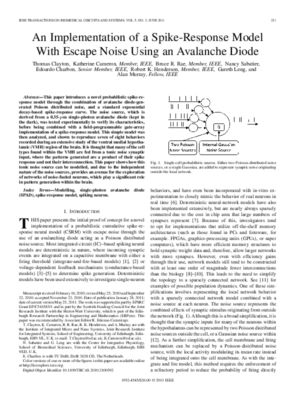
Fig. 1. Single-cell probabilistic neuron. Either two Poisson-distributed noise
sources, or a single Gaussian, are added to represent synaptic noise originating
outside the local network.
behaviors, and have even been incorporated with in-vitro experimentation to closely mimic the behavior of real neurons in
real time [6]. Deterministic neural-network models have also
been implemented extensively, but are nearly always sparsely
connected due to the cost in chip area that large numbers of
synapses represent [7]. Because of this, investigators tend
to opt for implementations that utilize off-the-shelf memory
architectures (such as those found in PCs and firmware, for
example. FPGAs, graphics-processing units (GPUs), or super
computers), which have more efficient memory structures to
hold synaptic weight data and, therefore, allow larger networks
with more synapses. However, even with efficiency gains
through their use, network models still tend to be constructed
with at least one order of magnitude fewer interconnections
than the biology [8]–[10]. This leads to the need to simplify
the topology to a sparsely connected network. See [11] for
examples of possible population dynamics. One of these simplifications involves representing the local network behavior
with a sparsely connected network model combined with a
noise source at each neuron. The noise source represents the
combined effects of synaptic stimulus originating from outside
the network (Fig. 1). Although this is a broad simplification, it is
thought that the synaptic inputs for many of the neurons within
the hypothalamus can be represented by two Poisson distributed
noise sources outside the cell, or a Gaussian noise source within
[12]. As a further simplification, the cell membrane and firing
mechanism can be replaced by a Poisson-distributed noise
source, with the local activity modulating its mean rate instead
of being integrated onto the cell membrane. As with the integrate and fire model, this method requires the enforcement of
a refractory period to reduce the probability of firing directly
1932-4545/$26.00 © 2011 IEEE
�232
IEEE TRANSACTIONS ON BIOMEDICAL CIRCUITS AND SYSTEMS, VOL. 5, NO. 3, JUNE 2011
after a spike event and, hence, remove events that correspond
to small interspike intervals.
Noise is widely used with neural networks. Within probabilistic structures, such as the Boltzmann machine [13], noise
can be used to escape local minimas and represent the natural
variability of the data. In spiking neural networks, it has been
observed that the mutual information transfer can be increased
by stochastic resonance [14]. In addition, Fusi [15] showed that
if stochastic learning takes place, the length of time that memories can be stored increases.
Creating a noise source with the required characteristics is
not straightforward. A review of techniques for creating noise
sources can be found in [16]; however, few are suitable for
very-large scale-integrated (VLSI) implementation. Alspector
et al. [17] required a noise source for a modified Boltzmann machine VLSI implementation but found that although amplifying
the thermal noise of a resistor was a good source of noise, highfrequency oscillations caused the noise generators to correlate.
They developed an alternative technique to produce Gaussian
noise that did not suffer from correlations, and was suitable for
VLSI implementation [18], but it was generated using a linear
feedback shift register and was therefore only pseudorandom.
If spiking noise is required, Chicca and Fusi showed how a randomly connected recurrent network can be used to generate a
stochastic spike train [19].
This paper focuses on the development and testing of a probabilistic cumulative spike response model with escape noise,
which utilizes the dark count of a single-photon avalanche diode
(SPAD) to represent the cell membrane and firing mechanism.
This paper shows that the dark count of a SPAD, when filtered
for trapped charge effects, can be considered a pure Poisson distributed noise source. Furthermore, multiple SPADs used in this
manner produce uncorrelated events, even when located next to
each other on the substrate. Finally, we show that many of the
single neuron behaviors recorded from the hypothalamic region
of the brain can be replicated by applying a cumulative spike
response mechanism to modulate the probability of avalanche
diode-generated events. Replicated behaviors include spike
adaptation, bursting, doublet, random, and regular activity.
The remainder of this paper is organized as follows. Section II
introduces the cumulative spike-response model, highlighting
its ties to observed biological phenomena. Section III introduces
the SPAD architecture, discusses dark count, and why it is a
suitable noise source, before presenting the method and results
of experimentation to determine the quality of the noise produced. Section IV presents the proof-of-concept combination
of the cumulative spike response (CSR) mechanism and SPAD
noise source to create an avalanche diode-fuelled neural model.
The method of implementation and results are presented, and
the limitations of this form of model are discussed. This paper
is drawn to a close by a brief conclusion.
II. INTRODUCTION TO SPIKE-RESPONSE MODELS
The spike-response model (SRM) [20]–[24] is an extension
of the leaky integrate-and-fire (IF) model, where the membrane
potential of the cell is derived from the time since the last action
potential initiation, and the time since each incoming synaptic
Fig. 2. Graphs showing the kernels that control the model’s response over time
to (a) an outgoing action-potential and (b) three incoming synaptic events. The
outgoing action-potential consists of an initial peak (the spike) followed by a refractory period which greatly decreases the probability of refiring. The incoming
synaptic events are represented by a single exponential decay (the red lines are a
best fit to different values of this exponential). (Both images are reprinted from
[24].)
event. The impact of the cells’ own action potential and incoming synaptic events is defined by two kernels that describe
the shape of their impact with time. In this way, the SRM introduces a measure of refractoriness to the IF model that describes
a combination of effects, such as increasing threshold, hyperpolarizing afterpotential, and post-action-potential reduced responsiveness
(1)
Equation (1) describes the membrane potential as a function
of time . The neuron fires when the membrane voltage crosses
, where
the dynamic threshold, also enforced by a kernel
is the firing time of the last spike. It is constructed through the
sum of the influence from the kernel that describes the shape of
the membrane potential, both during and postfiring
, and the
to the influence from each synaptic input
.
response
An example of the kernels and is shown in Fig. 2.
The advantage of this form of model is that it can be made to
produce a biologically realistic response to incoming synaptic
events, while still being extremely simple in structure. This
makes the SRM an ideal candidate for network models [25]
as well as being easily adaptable to experimental data [26].
However, the basic SRM cannot represent slow activity-dependent effects, of the order of seconds, which are involved in
slow bursting (such as the phasic firing patterns of vasopressin
cells [27]). The cumulative spike-response model (CSRM)
[28] provides the solution to this problem. Where the SRM is
only interested in the most recent action potential, the CSRM
calculates its membrane potential from the combined effects of
several spikes, with synaptic events treated in the same manner
as within the original SRM (2). is the times of all previous
firings
(2)
Both the adaptive exponential model [29] and Izhikevich’s
model [30], include cumulative adaptive elements within them.
However, these models were not used as only the spike-response
�CLAYTON et al.: IMPLEMENTATION OF A SPIKE-RESPONSE MODEL
elements, and not a firing mechanism, were required. In addition, as described later in Section II-B, two adaptive variables
(DAP and AHP) were essential for the reproduction of experimental VMH data, as opposed to the one (AHP) present in both
of the aforementioned models.
A. Noise and the SRM
The SRM and CSRM can be simplified by replacing the
synaptic input with a noise source, which then allows their
study through the cell’s probability of firing. This model,
which has been called a stochastic threshold model [23], can
now be analyzed analytically as a probability density function
(PDF) of the model’s ISI distribution. The same process can
be performed for CSRMs but the calculation of the PDF is
significantly more complex.
The most direct noise source implementation is to employ
two Poisson-distributed sources in the place of all synapses,
one to represent all excitatory presynaptic potentials (EPSPs),
and the other to represent the inhibitory ones (IPSPs). These
can be controlled to dictate the ratio (excitatory to inhibitory)
of incoming events. Alternatively, if control of this ratio is not
required, a Gaussian source may be instead implemented internally, as a diffusion approximation of many synaptic inputs. Finally, a Poisson-distributed source can be used as the output of
the neural model. With this implementation, the probability of
spike generation is modulated by the spike-response pattern to
create the natural refractory periods produced from real neurons. This implementation, which can be considered to be an
SRM with escape noise, has been chosen for our hardware implementation.
B. Probabilistic CSRM
The model presented in this paper is a CSRM with escape
noise, using a series of summed exponential decays to represent
the accumulation of all previous spike responses. Each exponential corresponds to an excitatory or inhibitory post-action-potential membrane dynamic (the hyperpolarizing after potential
(HAP) [31], depolarizing after potential (DAP), and after hyperpolarization (AHP) [27], [32]). The HAP is a brief hyperpolarization (half life 10 s of milliseconds) that sets the relative refractoriness of a cell after a spike—it can be modelled
well with an SRM. The AHP is a much smaller and slower (half
life—of the order of seconds) post-spike hyperpolarization that
accumulates with successive spikes—this cannot be modelled
with an SRM but instead requires a CSRM. The DAP characteristics fall between the two in magnitude and half life, and can be
modelled by an SRM. However, longer term behaviors, such as
phasic firing, require a CSRM since they can only be produced
through the creation and suppression of a plateau of summed
DAP activity. When combined with the noise-source control parameter, this creates a 7-D parameter space where pairs of parameters can be directly tied to the magnitude and duration of
specific identifiable intrinsic cell characteristics.
This form of model is computationally simple because the
model’s spike response is a sum of exponentials, where each
can be calculated at every time step by single multiplication. In
addition, the response to the entire spike history, instead of just
the most recent spikes, can be calculated at the same time using
233
the same method. This is because the overall spike response
over time is split by individual post-action-potential membrane
dynamics, which are described as
(3)
where
is the magnitude of the post-synaptic action potential
is the time constant of the membrane
membrane dynamic,
dynamic, the Dirac delta function approximates the effect of
spike production upon the membrane dynamic through the ad-sized step increase or decrease, and is the
dition of an
time of spike production. With fixed control parameters for
and
, the bulk of the function can be simplified prior to simulation in discrete time to a single multiplication and a possible
addition
(4)
where
is the size of the simulation time step, and
is the
Kronecker delta function which is equal to 1 when is equal to
.
The integration of balanced (50% excitatory, 50% inhibitory)
incoming synaptic noise on the membrane, combined with a
threshold firing mechanism, is represented by the probability
of a Poisson-distributed noise source generating a spike. The
spike-response pattern, generated by the summed exponential
decays representing a neuron’s HAP, DAP, and AHP, applies an
offset to the mean firing rate of the noise source and, therefore,
facilitates a refractory period in addition to the creation of more
complex firing patterns. This is described as
when
(5)
is the probability of spike generation for a given
where
time step. This is kept much smaller than 1 by reducing the size
of the time step. The time step used was 1 ms. Since most hypothalmic neurons fire at a rate much lower than 50 Hz,
should have a base value of less than 0.05.
,
, and
represent the current value of the individual exponentials
is a nonlinear transfer
that form the spike response, and
function that converts the spike response into a probability of
firing. The spike response is first combined with the base probbefore this function is applied. This funcability of firing
tion is explained in more detail in Section III since it is dependent on the Poisson-distributed random process.
The reason a Poisson-distributed noise source can be utilized
in this fashion is due to the similarity between recorded cell data
and a purely Poisson-distributed process. This can be shown by
using the hazard function [33], [34], which is a modification of
, where is the bin number of the ISI
the ISI histogram,
histogram. It is calculated as follows:
(6)
The hazard function represents the probability of a spike
event being generated at a given time interval since the previous event, provided that a subsequent event has not yet
�234
IEEE TRANSACTIONS ON BIOMEDICAL CIRCUITS AND SYSTEMS, VOL. 5, NO. 3, JUNE 2011
Fig. 3. Interspike interval (ISI) in five millisecond bins and hazard function
of data recorded from a randomly firing VMH cell (dashed line) and a Matlabgenerated Poisson spike train (solid line).
occurred. A Poisson-distributed process has a constant probability of producing an event irrespective of the time since the
previous event, which is shown as a flat distribution. Fig. 3
shows the hazard functions of a randomly firing neuron and
a Poisson-distributed noise source generated in Matlab. The
recorded neuronal pattern is similar except for a refractory
period immediately after a spike event, which is enforced to
protect the cell from death due to overactivity. This shows that
after this initial refractory period, the statistics are consistent
with a homogeneous Poisson process. Sabatier and Leng [35]
performed a study of cell-firing patterns recorded from the
VMH, and showed that when normalized by their mean firing
rate, they could be divided into nine distinct groups according
to their hazard functions. These groups, with the exception of
oscillatory behavior, are shown in Fig. 4. By altering the ratio
of the magnitudes and half lives of the exponential decays that
form the spike response, this paper shows that similar behaviors
can be generated from this Poisson-driven probabilistic CSRM.
No attempt was made to reproduce the oscillatory behavior
since it is thought to be a product of network phenomena, and
not intrinsic cell properties.
The bulk of the model complexity is tied to an easily conceptualized and computational simple membrane response to cell
activation. Since the spike response is the sum of three exponentially decaying variables, a solution could be constructed using
either digital or analog; however, for this proof of concept, a
digital implementation within an FPGA was chosen due to the
low development costs.
III. AVALANCHE DIODE-DRIVEN POISSON-DISTRIBUTED
NOISE SOURCE
A. Introduction to SPADs
The single-photon avalanche diode (SPAD) allows
single-photon detection through the action of avalanche breakdown in a - photodiode, reverse biased above its breakdown
voltage (Geiger mode). In Geiger mode operation, the gain of
a SPAD becomes virtually infinite and, with suitable biasing, a
transistor-transistor logic (TTL)-compatible pulse is produced
Fig. 4. Hazard function calculated from cell recordings during eight different
types of behavior [35].
upon detection of a single photon. The concept of the avalanche
photodiode was first proposed by Haitz et al. [36] and, in recent
years, much work has focused on implementing single-photon
avalanche diodes in a standard complementary metal–oxide
semiconductor (CMOS) process [37]–[40]. SPADs realized in
a foundry CMOS process were first demonstrated by Rochas et
al. in 2002 [41].
A diode biased beyond its reverse bias breakdown voltage
will remain in a quiescent state (zero current flowing) for a relatively long period of time (in the order of milliseconds). It is
the occurrence of a primary-free carrier within the high electric
field - junction that triggers an avalanche breakdown event
[42]. When operated as a photodetector, it is always hoped that
this primary-free carrier is generated as a result of an incident
photon. However, spurious breakdown events do occur due to
thermal- or tunnel-generated carriers and trapped charges.
If a free electron-hole pair is generated within the depletion
region of the - junction, the high electric field caused by
the large reverse bias voltage will accelerate the electrons and
holes toward the and regions, respectively. The accelerated
free electron and hole collide with static electron-hole pairs
in the junction, resulting in impact ionization. These newly
created free electrons and holes are subsequently accelerated,
resulting in further collisions and, hence, ionization events.
As the number of free electron-hole pairs increases, the current flowing through the SPAD exponentially increases until
quenching occurs.
�CLAYTON et al.: IMPLEMENTATION OF A SPIKE-RESPONSE MODEL
235
priate bias conditions. For the SPAD to operate in Geiger mode,
it must be biased above its breakdown voltage. The + anode
of the SPAD is therefore biased at a high negative voltage
[Fig. 5(b)]. The deep -well cathode is connected to a positive
power supply
, via a quench resistor.
The key is to ensure that the excess bias voltage across the
SPAD when in an armed state is equal to 3.3 V (for a 0.35- m
process). The excess bias voltage is defined as
(7)
Fig. 5. (a) Structure of the SPAD device. (b) SPAD with quench resistor.
Dark counts are non-photon-induced breakdown events and
are a function of detector area and temperature. The primary
causes of dark counts are thermal- or tunnel-generated carriers
in the diode - junction [42]. As such, the dark count rate
(DCR) of a SPAD is strongly temperature dependent and follows the temperature dependence of these mechanisms. As a
rule of thumb, the dark count doubles every 10 C [42]. Dark
count is also dependent on the reverse bias voltage placed across
the SPAD. As this voltage is increased, the SPADs sensitivity
increases, due to the higher electric field at the - junction increasing the likelihood of an avalanche breakdown event. However, the increased probability of breakdown also increases the
probability of a nonphoton-induced breakdown occurring. It is
this method of electron-hole pair generation that will be used as
the noise source.
After-pulsing is defined as spurious counts caused by carriers
temporarily trapped in the depletion region during a breakdown
event. After a short time, these charges are released, causing a
secondary Geiger pulse. The level of after-pulsing in a device
is dependent on the quality of the silicon (which defines the
trap concentration) and the number of carriers generated during
a breakdown event [43]. The number of carriers generated
is dependent on the parasitic capacitance of the diode and
the quench circuitry used. If the hold-off time of the quench
circuit is not long enough, trapped charges do not dissipate
and after-pulsing occurs. As quench time increases, the correlation between the initial pulse and after-pulses decreases.
After-pulsing also shows an inverse temperature dependence,
increasing as temperature decreases [44].
SPAD Structure and Biasing: The SPAD detector implemented in this project consists of a circular dual-junction
structure: + anode/deep -well/ -substrate [Fig. 5(a)]. The +
anode/deep -well junction forms the avalanche multiplication
region where the Geiger breakdown occurs. The -well/ -substrate junction allows the + anode to be biased independently
from the substrate and prevents electrical crosstalk. A -well
guard-ring surrounds the + anode to prevent premature breakdown [45]. The device has a diameter of 6 m, resulting in an
active area of 28.27 m .
To ensure the SPAD detector’s compatibility with standard
CMOS circuitry, the biasing of the SPAD must be carefully considered. The logic levels of the 0.35- m process used in this
project were 0 V (logic 0) and 3.3 V (logic 1). Therefore, it had
to be ensured that the output transition of the SPAD on breakdown had a 3.3-V swing. This is achieved by setting up appro-
where
is the SPAD excess bias voltage, and
is the
reverse bias breakdown voltage of the diode. At the onset of
Avalanche breakdown in the photodiode, current begins to flow
in the device. As this current increases, the voltage dropping
across the quench resistor increases, thus lowering the reverse
bias voltage across the diode. This process continues until the
diode is brought out of Geiger mode and the avalanche process
is halted. According to (7), the transition required to bring the
. As the curSPAD out of avalanche breakdown is equal to
rent through the diode is reduced, the voltage dropping across
the quench resistor is reduced. In turn, the photodiode reverse
bias voltage increases until the diode returns to Geiger mode operation. The SPAD is now rearmed and ready to detect the next
photon. The quench resistor is sized so that the voltage transition
seen at the SPAD output [
, Fig. 5(b)] during this process
is compatible with standard CMOS logic cells.
If the reverse bias across the SPAD is insufficient, the SPAD
will never breakdown. Conversely, if the reverse bias voltage is
too high, the SPAD will be in permanent breakdown. For the
SPAD used in this project, the minimum reverse bias voltage
was found to be approximately 20.8 V. The SPAD went into
permanent breakdown at voltages above approximately 24.05 V.
B. Experimental Setup
To test the viability of avalanche diodes as a source of
Poisson-distributed random events, an application-specific
integrated circuit (ASIC), which included nine independently
wired SPADs, was shielded from all light sources and analyzed.
This analysis focused on how changes to the off-chip bias
voltage affected the mean firing rate as well as determining
if there was any cross correlation between adjacent SPADs.
The correlations could be caused by optical or electrical
crosstalk [45]. These types of crosstalk would both increase
the likelihood of neighboring SPADs firing, but another type of
correlation could be present. When an SPAD fires, quenching
current is drawn from
since this is a global signal and any
variation in it will affect the probability of firing all of the other
SPADs. Any of these would be highly detrimental to any future
neural-network implementation.
SPAD events were collected via an FPGA1 and time-stamped
before being passed to custom software via USB for analysis.
Each timestamp (24 b) was accompanied by an address (8 b).
The FPGA was clocked at 200 MHz, well above the Nyquist frequency for these particular SPADs (maximum output frequency
of 30 MHz).
1The
FPGA was on an Opal Kelly XEM 3010 Development Board.
�236
IEEE TRANSACTIONS ON BIOMEDICAL CIRCUITS AND SYSTEMS, VOL. 5, NO. 3, JUNE 2011
Fig. 6. Interspike interval (ISI), in five millisconds bins, and hazard function
of (a) a Matlab-generated Poisson spike train, reproduced from Fig. 3 and (b)
recorded dark count events from a single SPAD.
Fig. 8. Three hazard functions. The dashed line marked with triangles is the
hazard function of a SPAD-generated spike train. The dotted line marked with
asterisks is the hazard function calculated from the inter spike intervals between
a Matlab-generated Poisson spike train and the spike train from the SPAD. The
solid line is the hazard function between two spike trains with artificial correlations inserted between them. The increase in probability of firing 200 ms after
an event on the previous spike train is clearly visible.
Fig. 7. Mean frequency of the dark count when VOP is altered. Below 20.5 V,
there is an approximately linear relationship between voltage and probability of
firing.
C. Results
The first test undertaken was to look at the events recorded
from a single SPAD and plot the ISI distribution and corresponding hazard function in order to verify that the SPAD-generated dark events were indeed Poisson distributed. The
recorded events were first preprocessed to remove the spikes
caused by after-pulsing. Any spike that occurred within 200 s
of the previous event was deleted from the spike train. Fig. 6
shows the results and a comparison with Fig. 3 indicates that
a SPAD can indeed produce a Poisson-distributed spike train.
To further test the spike train, a negative exponential curve
was fitted to the ISI histogram data, bin width 5 ms, and the
,
coefficient of variation (CV), defined as
was also calculated. The curve was fitted with an adjusted
value of 0.9966 and the CV was 1.0195 (a perfect Poisson spike
train has a value of 1 for both). These results, when combined
with the near flatness of the hazard function in Fig. 6(b), give
confidence that the spike trains can be regarded as Poisson.
The mean frequency of the spike train can be altered by
VOP—the large negative voltage applied to the SPAD. Tests
were run to find the range of frequencies that could be achieved.
The mean dark count was recorded by the FPGA for voltages
ranging from 17.71 v to 21 V. The results are shown in Fig. 7.
This mean dark count can be interpreted as the probability
of firing given a varying
. This allows us to implement
representing
.
(5) with
Above 20.5 V, the electric field across the SPAD becomes so
high that the SPAD begins to break down laterally, in a more
regular manner, and, therefore, the spike train loses its Poisson
distribution. The results show that we can achieve a mean
frequency of up to 40 Hz which is a good range for single
neuron models. An array of 1024 of these SPADs has been
reported in [46]. The event readout is address based, allowing
the spike trains to be merged if a faster frequency is required.
It is also important to determine that the Poisson-distributed
spike trains from neighboring SPADs are independent. If two
Poisson-distributed spike trains are independent, the interspike
interval between these two trains will also be Poisson. To illustrate this, three spike trains were generated: A) a recorded spike
train from a SPAD that was preprocessed to remove the effects
of after-pulsing. This was done by removing any spike that occurred within 200 s of the preceeding pulse; B) A Matlab-generated Poisson spike train with a mean frequency of 15.5 Hz;
and C) a spike train recorded from another SPAD which had a
10% artifical correlation to A added to it. Fig. 8 shows three different hazard functions created from these spike trains. The line
marked with triangles is the hazard function of spike train A. As
expected, the hazard function is flat, indicating a Poisson-distributed spike train. The Matlab-generated Poisson spike train
(B) was then compared to the train from the SPAD (A). The ISI
from every spike in B to the next spike in A was calculated and
the hazard function determined. This result is shown by the line
marked with asterisks. Since the spike trains are independent,
the hazard function is flat and has the same probability of firing
as spike train A. Finally, the hazard function between trains C
and A was calculated and is shown as the solid line in Fig. 8.
The peak in the hazard function clearly indicates a correlation
is present.
To test that the spike trains were not correlating, the same
process was performed on data recorded from eight neighboring
�CLAYTON et al.: IMPLEMENTATION OF A SPIKE-RESPONSE MODEL
237
TABLE I
ADJUSTED R VALUES AFTER CURVE FITTING AND THE COEFFICIENT OF VARIATION (CV)
calculated—the solid lines in Fig. 9. The ISI between all possible combinations of spike trains was also calculated and then
the hazard functions generated. The worst case (max and min)
hazard function to a particular SPAD was calculated and is
shown by the band. No high peaks in the hazard functions were
detected, indicating that the spike trains can be regarded as
independent. The curve fitting and coefficent of variation tests
were performed for all the possible ISI combinations as further
evidence, and the results are shown in Table I. The Adjusted
and CV for the spike trains recorded from the SPADs are
shown in bold. The results for the ISIs between spike trains are
all close to one, providing a high level of certainty of the spike
trains’ independence. The results for the SPAD generated spike
trains B, C, D, and G are further away from one. This is due
to the after-pulsing effect not being entirely removed by the
200- s preprocessing of the spike train. The effect of the after
pulsing is clearly visible in Fig. 9, the probability of firing for
SPAD B, C, D, and G is much higher just after the previous
event. In a neural application, this does not pose a problem as a
larger refractory period can, and will be, applied.
D. Summary
The three results presented in the previous section all underline
that SPADs can produce Poisson-distributed spike trains, and that
the spike trains from neighboring SPADs do not correlate.
The frequency of these spike trains can be controlled by the bias
voltage VOP. Biologically plausible frequencies of up to 40 Hz
can be achieved and, as each spike train is independent, they
can be added together should faster frequencies be required.
Fig. 9. The spike trains for 8 SPADS (A-H) were recorded simultaneously.
The blue line in each graph shows the hazard function of each spike train. The
green envelope shows the range of hazard functions of the ISI between spike
trains. The probability of firing remains the same; therefore, no correlations are
present. The initial hazard function for SPADS B, C, D, and G are high due
to the after-pulsing effect. This is an undesirable effect but can be removed by
applying a refractory period to the SPAD [46].
SPADs (A–H). Each train was individually preprocessed to
remove the effects of after-pulsing, and had its hazard function
IV. PROBABILISTIC CUMULATIVE SPIKE-RESPONSE MODEL
This section introduces the proof-of-concept implementation
of an avalanche diode-based neuron. An implementation of the
model presented in Section II is evaluated through the attempted
replication of the eight preclassified VMH cell behaviors. We
show that seven of the eight behaviors are reproducible in addition to longer term behaviors such as spike adaptation and
bursting.
�238
IEEE TRANSACTIONS ON BIOMEDICAL CIRCUITS AND SYSTEMS, VOL. 5, NO. 3, JUNE 2011
Fig. 10. Experimental setup. (a) An Opal Kelly FPGA board is connected by
the universal serial bus to a PC, and configured with the ability to capture, timestamp, and stream SPAD events back to the PC, implement the CSRM, and
send configuration data to the DAC every 1 ms. (b) The negative bias voltage is
generated by placing the fixed power supply between the DAC output (positive
terminal) and the global VOP input to the SPAD IC (negative terminal). (c) The
SPAD IC only has a single SPAD monitored.
A. Implementation
The neural model was implemented through the combination
of a heavily light shielded SPAD and an FPGA-controlled 5-V
8-b digital-to-analog converter (DAC), see Fig. 10. This DAC
was placed to modulate VOP between 20.5 V and 16.5 V, the
region that produces an almost linear relationship between mean
dark count and VOP. This thereby allows the FPGA to linearly
alter the probability of producing an event.
Within the FPGA, a state machine controls a cumulative
spike-response (CSR) mechanism, which, in turn, controls
the digital input to the VOP DAC. The model, which is a
discrete implementation with a 1-ms time step, consists of three
variables, each under a different constant decay, representing
the HAP, DAP, and AHP of the neural model. If the SPAD
produced one or more action potentials during the previous
iteration (1 ms of time), a step increase or decrease is applied
to each variable. These variables are combined with an offset
variable to determine the final voltage produced by the DAC
(8)
The offset variable is used to position “0” so that the summed
effects of the DAP or AHP will not cause clipping (See Fig.
11). The HAP is much larger than the DAP and AHP; hence,
it is presumed that the HAP will clip. However, this is not a
problem, as the clipping will force the SPAD into a region where
avalanching is extremely unlikely to occur, hence enforcing a
natural refractory period.
B. Results
The seven model control parameters (the magnitude and half
life of the three decays, plus the offset) were tuned by hand to
create a spike response that, when combined with the Poisson
nature of the SPAD, would reproduce the likenesses of the patterns recorded from the VMH [35]. See Fig. 11 for an example
of a generated spike response. The seven successful configurations are shown in Fig. 12, overlaid with their biological counterparts. The solid lines are the data generated by our model.
The data recorded from the VMH are shown with a dashed line.
One of the recorded biological behaviors (regular firing) was
found to be extremely difficult to recreate, with Fig. 13 showing
Fig. 11. Spike response pattern. This pattern, recorded from the circuit implementation, consists of the summation of three exponential decays—HAP, DAP,
and AHP. The pattern is centered within the 5 V peak-to-peak region of the DAC
by the offset parameter. Any value outside this region will be clipped by either
the upper or lower limit.
the closest match found. While this trace has been confirmed
as regular firing, it was only possible through the implementation of bursting behavior caused by DAP summation. This, in
essence, created a composite non-homeostatic behavior, where
the hazard is the combination of ISI distributions drawn from
the model when it is in its elevated and suppressed states.
The cause of the model’s inadequacy is rooted in the random
nature of the SPAD’s dark count, and how this is manipulated
to produce different probabilities of firing. The probabilistic
model uses the Poisson-distributed noise source to generate
spike events, where the spike-response pattern is used to alter
the mean firing rate of the noise source with time. This alters
the probability of producing a spike event with respect to all
preceding events. In this way, the spike response is a direct
representation of the resulting hazard function. This also means
that behaviors can only be produced if the shape of the hazard
can be constructed from the three exponential decays. The
hazard of the regular firing behavior consists of a refractory
period, which dictates the mean firing rate, followed by a large
DAP that falls sharply to a much lower probability of firing
(determined by the base firing rate of the SPAD, see Fig. 13).
Initially, it was thought that this behavior could be created
though the combination of two exponentials; a large negative
going exponential to represent the refractory period, and a positive one to create a brief period of time directly after the refractory period that greatly elevates the probability of firing.
However, because the model applies a step increase to all exponentials at the same time, the DAP must have a longer half life
than the HAP to have a positive effect on the spike response.
This poses several problems; First, it is not possible to create
a sharp enough DAP decay while maintaining the refractory
period. Second, since the half life of the DAP is greater than
that of the HAP, and the model takes account of all previous
activity, DAP summation can occur. This promotes a rudimentary bursting behavior, as shown in Fig. 13, where a self-sustaining plateau is formed that may randomly collapse and, as a
result, longer interspike intervals can be generated randomly by
the Poisson-distributed process.
�CLAYTON et al.: IMPLEMENTATION OF A SPIKE-RESPONSE MODEL
239
Fig. 12. Data from the SPAD SRM are the solid line. The dashed line is the VMH cell data. (a) Random behavior: characterized by a sharp HAP, to prevent
immediate reactivation; and no further dynamics. (b) Doublet behavior: characterized by an extremely fast HAP followed by a sharp, but large DAP, to promote
reactivation, and, hence, doublet behaviour. (c) Broad behavior: characterized by a slow but constant increase in probability of firing until a plateau is met. (d)
Doublet broad behavior: characterized by a similar distribution to the broad behavior, but with a greatly increased chance of reactivation in the form of a doublet.
(e) Long-tailed type 1 behaviour: characterised by a broad peak probability of firing before falling to a lower level. (f) Long-tailed Type 2 behaviour: characterized
by the distinctive shape of the rise to constant probability of firing. This shape is caused by the combination of a low magnitude HAP and a shorter half life AHP
(100 s of microseconds). (g) Slow DAP behavior: characterized by a small initial peak of activity before stabilizing at a constant probability of firing.
Fig. 13. (a) Regular behavior. The model allows that either the length of the
refractory period or the decay rate after the peak activity be correct. This limitation means that the CSRM cannot truly recreate random firing activity. The
data from the SPAD SRM are the solid line. The dashed line is the VMH cell
data. (b) The spike rate was recorded from the SPAD SRM over a period of 100
s while attempting to recreate regular firing. Note the bursting behavior.
Ultimately, the recreation of regular firing behavior is impossible through the summation of exponentially decaying variables with synchronized step increases. However, if the correct
spike-response pattern was created, then a true regular firing
pattern could be recreated. This could be done by delaying the
step increase of the DAP, thereby allowing it to have a shorter
half life while still allowing it to have an effect on the resulting
spike-response pattern, see Fig. 14.
C. Spike Adaptation and Bursting
Fig. 15 shows how the model can be made to produce bursting
activity. This behavior is possible because the method used to
construct the spike-response pattern, being cumulative, takes account of all previous activity. Therefore, the model can create
Fig. 14. Original and alternative SRM. In the alternative SRM, only the DAP
is changed. Its half life is reduced and the step increase is only applied 100 ms
after the spike event. The allows a long refractory period and a steep roll-off to
be modelled.
longer term behaviors through the summation and interaction of
the positive and negative going exponential decays.
In the case of spike adaptation, the longer term inhibitory
effects of the AHP summate over multiple spike events, providing a negative feedback mechanism that naturally reduces
the probability of firing, see Fig. 15. The DAP can be configured to provide the opposite effect in the form of a short-term
positive feedback mechanism. When combined with the longer
term AHP, both of these effects interact to produce bursting,
see Fig. 15. The DAP, having a larger magnitude, will accumulate more quickly, thereby further increasing the probability of
firing. However, after a period of time, the AHP will become
�240
IEEE TRANSACTIONS ON BIOMEDICAL CIRCUITS AND SYSTEMS, VOL. 5, NO. 3, JUNE 2011
Fig. 15. Burst dynamics, recorded from the SPAD SRM, caused by interaction
between the DAP and AHP. (a) The DAP accumulates rapidly, providing positive feedback. (b) The AHP magnitude becomes comparable with and, therefore,
collapses the DAP plateau. (c) Period of silence while the AHP decays. Once
this occurs, the cycle can repeat.
closer in magnitude and slow the firing rate to such a degree that
the DAP summation will collapse. At this stage, the accumulated AHP remains, hence firing is halted until the AHP decays
enough that the SPAD can fire again, and the cycle can repeat.
D. Summary
During this section, the Poisson-distributed SPAD output was
modified with time by the inclusion of a CSR mechanism that
consists of three exponential decays representing the HAP, DAP,
and AHP intrinsic cell properties. This model was applied to the
bias voltage and, therefore, altered the probability of firing with
respect to previous spike events.
To evaluate this system, the model was adapted by hand to
reproduce eight neural behaviors that were prerecorded from
the VMH within the hypothalamus. Of these eight behaviors,
seven were easily reproduced alongside spike adaptation and
bursting, with only the regular firing behavior proving difficult
to replicate.
This inadequacy was found to be caused by a limitation with
the model, which cannot create a spike response with a sharper
DAP decay rate than that of the HAP, which is responsible for
enforcing the postfiring refractory period. This is not to say that
this regular firing cannot be recreated; the hazard function of
regular firing could be converted directly into a noncumulative
SRM kernel that would naturally recreate this pattern. However,
the removal of the cumulative nature of the CSRM would result in the inability to produce spike adaptation and bursting
behavior.
V. CONCLUSION
This paper has introduced the SPAD device as a source of
Poisson-distributed noise. We have shown that the dark count of
an avalanche diode is: Poisson distributed; independent of other
avalanche diodes in near proximity; and that the mean firing rate
of the dark count is approximately linearly proportional to the
magnitude of the negative bias voltage.
We then showed how this relationship can be utilized to implement a simple cumulative spike-response model with escape
noise. This implementation represents a significant abstraction
away from traditional models, where synaptic noise is integrated
on a membrane, which then interacts with a deterministic firing
mechanism. This is not to say that we could not implement
such a model with SPAD noise sources; indeed, such a system
could easily be constructed using multiple SPADs as independent synaptic inputs. However, since the long-term goal of this
paper is to explore network activity on silicon, it is more practical to assume that the networks we aim to explore are fed by
balanced tonic noise, and use a single device to represent the
entire synaptic input and neuron.
Our model was tested and was capable of reproducing seven
out of eight broad categories of single-cell spiking behaviors
similar to those captured from the VMH region of the brain, as
well as spike adaptation and bursting. We have explored the limitations of this model and show that regular firing activity is difficult to implement. This is, however, not a failure of the neural
avalanche diode-based method, but rather a limitation of the
model, which simply cannot produce a spike response of sufficient complexity to reproduce this regular behavior. The probability of firing for a given postfiring period of time can be derived
empirically from the recorded interspike interval data in the
form of hazard functions. This information can then be used to
construct a more complex noncumulative spike-response kernel
which could produce any desired behavior, including regular.
Although the work in this paper was motivated by the need
for independent noise sources in a single-neuron spike-response
model, the opportunities for avalanche-diode-generated noise
are far wider. Models of spiking networks involving multiple
noise sources will be made more compact, faster, and, thus, usable in the laboratory environment by the technology in this
paper. Furthermore, noise-mediated effects, such as stochastic
resonance [14], and noise-driven artificial neural networks, such
as the Boltzmann machine [13], and its derivatives [47] need independent noise sources. If the promise of, for example, the continuous restricted Boltzmann machine as an embedded sensorfusion architecture [48] is to be fulfilled, multiple, integrated,
compact, analog noise sources will be required. The SPAD-derived device described in this paper takes a fist step toward that
hitherto-elusive goal.
A. Future Work
This work was carried out using a SPAD which was designed
for low-light imaging tasks, such as florescent lifetime calculation [49]. The device has therefore been designed with photodetection in mind and, hence, has a large surface area to catch as
many photons as possible. We do not require this detection. In
fact, during this proof-of-concept study, the entire SPAD chip
was heavily shielded from all light sources. Therefore, future
work would first entail the design of an avalanching device designed specifically for our application. This device would be designed to have a large linear range of dark count rates to allow
the more complex behaviors to be recreated. In addition, we
would like to have a way of altering the probability of firing
via a method that does not require rapid modification of a large
negative voltage.
Ultimately, we would like to integrate the spike-response
model, which is currently held within the FPGA and DAC,
�CLAYTON et al.: IMPLEMENTATION OF A SPIKE-RESPONSE MODEL
alongside the avalanche diode, to create an instantaneous
probabilistic neural element that will allow the investigation of
network behaviors with probabilistic systems, and provide a
possible avenue for integration with biology.
ACKNOWLEDGMENT
The authors would like to thank K. Muir for his help with the
test board and general understanding of the SPAD. Dave Laurenson suggested the method for proving the independence of
the spike trains. The technical support of Europractice is gratefully acknowledged.
REFERENCES
[1] G. Indiveri, “A low-power adaptive integrate-and-fire neuron circuit,”
in Proc. IEEE Int. Symp. Circuits and Systems, May 2003, vol. IV, pp.
820–823.
[2] A. Bofill-i-Petit and A. F. Murray, “Synchrony detection and amplification by silicon neurons with STDP synapses,” IEEE Trans. Neural
Netw., vol. 15, no. 5, pp. 1296–1304, Sep. 2004.
[3] M. Mahowald and R. Douglas, “A silicon neuron,” Nature, vol. 354,
pp. 515–518, 1991.
[4] J. Wijekoon and P. Dudek, “A CMOS circuit implementation of
a spiking neuron with bursting and adaptation on a biological
timescale,” in Proc. IEEE Biomedical Circuits and Systems Conf.,
2009, pp. 193–196.
[5] K. Rice, M. Bhuiyan, T. Taha, C. Vutsinas, and M. Smith, “FPGA
implementation of Izhikevich spiking neural networks for character
recognition,” in Proc. Int. Conf. Reconfigurable Computing and
FPGAs, 2009, pp. 451–456.
[6] S. Saïghi, Y. Bornat, J. Tomas, and S. Renaud, “Neuromimetic ICs
and system for parameters extraction in biological neuron models,”
in Proc. IEEE Int. Symp. Circuits and Systems, May 2006, pp.
4207–4211.
[7] J. Schemmel, J. Fieres, and K. Meier, “Wafer-scale integration of
analog neural networks,” in Proc. IEEE Int. Joint Conf. World Congress on Computational Intelligence, 2008, pp. 431–438.
[8] J. M. Nageswaran, N. Dutt, J. L. Krichmar, A. Nicolau, and A. V.
Veidenbaum, “A configurable simulation environment for the efficient
simulation of large-scale spiking neural networks on graphics processors,” Neural Netw., vol. 22, no. 5–6, pp. 791–800, 2009.
[9] D. F. M. Goodman and R. Brette, “Brian: A simulator for spiking neural
networks in python,” Frontiers Neuroinf., vol. 2, 2008.
[10] M. Djurfeldt, M. Lundqvist, C. Johansson, M. Rehn, O. Ekeberg,
and A. Lansner, “Brain-scale simulation of the neocortex on the IBM
Blue Gene/L supercomputer,” IBM J. Res. Develop., vol. 52, no. 1, pp.
31–41, 2008.
[11] N. Brunel, “Dynamics of sparsely connected networks of excitatory
and inhibitory spiking neurons,” J. Comput. Neurosci., vol. 8, no. 3,
pp. 183–208, May 2000.
[12] G. Leng, C. H. Brown, P. M. Bull, D. Brown, S. Scullion, J. Currie,
R. E. Blackburn-Munro, J. Feng, T. Onaka, J. G. Verbalis, J. A. Russell, and M. Ludwig, “Responses of magnocellular neurons to osmotic
stimulation involves coactivation of excitatory and inhibitory input: An
experimental and theoretical analysis,” J. Neurosci., vol. 21, no. 17, pp.
6967–6977, 2001.
[13] G. E. Hinton and T. J. Sejnowski, “Learning and relearning in Boltzmann machines,” in Parallel Distributed Processing: Explorations in
the Microstructure Of Cognition. Cambridge, MA: MIT Press, 1986,
vol. 1, Foundations, pp. 282–317.
[14] G. Deco and B. Schürmann, “Stochastic resonance in the mutual information between input and output spike trains of noisy central neurons,”
Phys. D, vol. 117, no. 1–4, pp. 276–282, 1998.
[15] S. Fusi, “Hebbian spike-driven synaptic plasticity for learning patterns
of mean firing rates,” Biol.Cybern., vol. 87, pp. 459–470, 2002.
[16] S. J. Upadhyaya, “Noise generators,” in Wiley Encyclopedia of Electrical and Electronics Engineering, J. G. Webster, Ed. New York:
Wiley, 1999, pp. 384–392.
241
[17] J. Alspector, B. Gupta, and R. B. Allen, “Performance of a stochastic
learning microchip,” in Advances in Neural Information Processing
Systems. San Mateo, CA: Morgan Kaufmann, 1989, vol. 1, pp.
748–760.
[18] J. Alspector, J. Gannett, S. Haber, M. Parker, and R. Chu, “A VLSIefficient technique for generating multiple uncorrelated noise sources
and its application to stochastic neural networks,” IEEE Trans. Circuits
Syst., vol. 38, no. 1, pp. 109–123, Jan. 1991.
[19] E. Chicca and S. Fusi, “Stochastic synaptic plasticity in deterministic
aVLSI networks of spiking neurons,” in Proc. World Congr. Neuroinf.,
2001, pp. 468–477.
[20] W. Gerstner, R. Ritz, and J. L. van Hemmen, “Why spikes? Hebbian
learning of time-resolved excitation patterns,” Biol. Cybern., vol. 69,
pp. 503–515, 1993.
[21] W. M. Kistler, W. Gerstner, and J. L. van Hemman, “Reduction of
Hodgkin-Huxley equations to a threshold model,” Neural Comput., vol.
9, pp. 1069–1100, 1997.
[22] R. Jolivet, T. J. Lewis, and G. W, “The spike response model: A
framework to predict neuronal spike trains,” in Proc. Int. Conf. Artifical Neural Networks and Neural Information Processing, 2003, vol.
2714, pp. 846–853.
[23] W. Gerstner and W. Kistler, Spiking Neuron Models: Single Neurons,
Populations, Plasticity. Cambridge, MA: Cambridge Univ. Press,
2002.
[24] W. Gerstner, “Spike-response model,” Scholarpedia, vol. 3, no. 12, p.
1343, 2008.
[25] W. Gerstner, “Population dynamics of spiking neurons: Fast transients,
asynchronous states and locking,” Neural Comput., vol. 12, no. 1, pp.
43–89, 2000.
[26] R. Jolivet, A. Rauch, H.-R. Lüscher, and W. Gerstner, “Integrate-and-fire models with adaptation are good enough: Predicting
spike times under random current injection,” in Advances in Neural
Information Processing Systems. : MIT Press, 2006, vol. 18, pp.
595–602.
[27] P. Roper, J. Callaway, and W. Armstrong, “Burst initiation and termination in phasic vasopressin cells of the rat supraoptic nucleus: A
combined mathematical, electrical and calcium fluorescence study,” J.
Neurosci., vol. 24, no. 20, pp. 4818–4831, 2004.
[28] W. Gerstner, R. Kempter, J. L. van Hemmen, and H. Wagner, “A neuronal learning rule for sub-millisecond temporal coding,” Nature, vol.
383, pp. 76–78, Sep. 5, 1996.
[29] R. Brette and W. Gerstner, “Adaptive exponential integrate-and-fire
model as an effective description of neuronal activity,” J. Neurophysiol., vol. 94, no. 5, pp. 3637–3642, 2005.
[30] E. Izhikevich, “Simple model of spiking neurons,” IEEE Trans. Neural
Netw., , vol. 14, no. 6, pp. 1569–1572, Nov. 2003.
[31] R. D. Andrew and F. E. Dudek, “Intrinsic inhibition in magnocellular
neuroendocrine cells of rat hypothalamus,” J. Physiol., vol. 353, pp.
171–185, 1984.
[32] P. Roper, J. Callaway, T. Shevchenko, R. Teruyama, and W. Armstrong, “AHP’s, HAP’s and DAP’s: How potassium curents regulate
the excitability of rat supraoptic neurones,” J. Comput. Neurosci., vol.
15, pp. 367–389, 2003.
[33] R. D. Luce, Response Times: Their Role in Inferring Elementary
Mental Organization. Oxford, U.K.: Oxford Univ. Press, 1986.
[34] P. Janssen and M. N. Shadlen, “A representation of the hazard rate
of elapsed time in macaque area LIP,” Nature Neurosci., vol. 8, pp.
234–241, 2005.
[35] N. Sabatier and G. Leng, “Spontaneous discharge characteristic of neurons in the ventromedial nucleus of the rat hypothalamus in vivo,” Eur.
J. Neurosci., vol. 28, no. 4, pp. 693–706, 2008.
[36] R. Haitz, “Studies on optical coupling between silicon p-n junctions,”
Solid-State Electron., vol. 8, pp. 417–425, 1965.
[37] H. Finkelstein, M. J. Hsu, and S. C. Esener, “STI-bounded singlephoton avalanche diode in a deep-submicrometer CMOS technology,”
IEEE Electron Device Lett., vol. 27, no. 11, pp. 887–889, Nov. 2006.
[38] D. Stoppa, L. Pancheri, M. Scandiuzzo, L. Gonzo, G. F. Betta, and
A. Simoni, “A CMOS 3-d imager based on single photon avalanche
diode,” IEEE Trans. Circuits Syst., vol. 54, no. 1, pp. 4–12, Jan. 2007.
[39] M. Gersbach, C. Niclass, E. Charbon, J. Richardson, R. Henderson,
and L. Grant, “A single photon detector implemented in a 130 nm
cmos imaging process,” in Proc. 38th Eur. Solid-State Device Research
Conf., Sep. 15–19, 2008, pp. 270–273.
�242
IEEE TRANSACTIONS ON BIOMEDICAL CIRCUITS AND SYSTEMS, VOL. 5, NO. 3, JUNE 2011
[40] M. A. Marwick and A. G. Andreou, “Single photon avalanche photodetector with integrated quenching fabricated in tsmc 0.18 � 1.8
v CMOS process,” Electron. Lett., vol. 44, no. 10, pp. 643–644, May
2008.
[41] A. Rochas, A. Pauchard, P. A. Besse, D. Pantic, Z. Prijic, and R.
Popovic, “Low-noise silicon avalanche photodiodes fabricated in
conventional CMOS technologies,” IEEE Trans. Electron Devices,
vol. 49, no. 3, pp. 387–394, Mar. 2002.
[42] S. M. Sze, Physics of Semiconductor Devices. New York: Wiley-Interscience, 1981.
[43] S. Cova, A. Lacaita, and G. Ripamonti, “Trapping phenomena in
avalanche photodiodes on nanosecond scale,” IEEE Electron Device
Lett., vol. 12, no. 12, pp. 685–687, Dec. 1991.
[44] J. C. Jackson, D. Phelan, A. P. Morrison, R. M. Redfern, and A. Mathewson, “Toward integrated single-photon-counting microarrays,” Opt.
Eng., vol. 42, pp. 112–118, 2002.
[45] C. Niclass, M. Sergio, and E. Charbon, “A single photon avalanche
diode array fabricated in deep-submicron CMOS technology,” in Proc.
Design, Automation and Test in Europe, Mar. 6–10, 2006, vol. 1, pp.
1–6.
[46] K. Cameron, T. Clayton, B. Rae, A. Murray, R. Henderson, and E.
Charbon, “Poisson distributed noise generation for spiking neural applications,” in Proc. IEEE Int. Symp. Circuits and Systems, 2010, pp.
365–368.
[47] H. Chen and A. Murray, “Continuous restricted Boltzmann machine
with an implementable training algorithm,” Proc. Inst. Elect. Eng.,
Vis., Image and Signal Process., vol. 150, no. 3, pp. 153–158, Jun.
2003.
[48] T. Tang, H. Chen, and A. Murray, “Adaptive, integrated sensor processing to compensate for drift and uncertainty: A stochastic ‘neural’
approach,” Proc. Inst. Elect. Eng. Nanobiotechnology,, vol. 151, no. 1,
pp. 28–34, Feb. 2004.
[49] B. R. Rae, K. R. Muir, Z. Gong, J. McKendry, J. M. Girkin, E. Gu, D.
Renshaw, M. D. Dawson, and R. K. Henderson, “A cmos time-resolved
fluorescence lifetime analysis micro-system,” Sensors, vol. 9, no. 11,
pp. 9255–9274, 2009.
m
Thomas Clayton was born in 1981 in Surrey, U.K.
He received the M.Eng. degree in electrical and electronic engineering and the Ph.D. degree in electronic
engineering and neuroscience from The University
of Edinburgh, Edinburgh, U.K., in 2005 and 2009,
respectively.
His Ph.D. project and current work integrates
elements from electronic engineering, computer
science, mathematics, and experimental and computational neuroscience, with his published works
touching on graphics-processing unit and field-programmable gate-array-based hardware acceleration, evolutionary algorithms,
probabilistic computational modeling, and exploration of the hippocampus
and its interaction with the endocrine system. Currently, he holds research
posts within the Centre for Integrative Physiology, the Institute for Perception,
Action and Behavior, and the Institute for Integrated Micro and Nano Systems,
all within the University of Edinburgh.
Katherine Cameron (S’04–M’06) was born in Edinburgh, U.K., in 1979. She received the M.Eng. degree
(Hons.) in electronics and the Ph.D. degree in neuromorphic engineering from The University of Edinburgh, Edinburgh, in 2002 and 2007, respectively.
Currently, she is a Research Associate at the
School of Engineering. Her current research interests include bioinspired engineering solutions to
analog computation imperfections, mixed-signal
very-large-scale integrated design, and neural
computation.
Bruce R. Rae (M’08) was born in 1983 in Aberdeen,
U.K. He received the M.Eng. and Ph.D. degrees in
electrical and electronic engineering from The University of Edinburgh, Edinburgh, U.K., in 2005 and
2009, respectively.
During his Masters degree, he was with ST Microelectronics Imaging Division. His Ph.D. project focused on the design and implementation of a lowcost, miniaturized complementary metal–oxide semiconductor (CMOS)-based microsystem for time-resolved fluorescence analysis. As of 2008, he was a
Postdoctoral Research Associate at the Institute for Integrated Micro and Nano
Systems which is part of the School of Engineering, The University of Edinburgh. His research interests include the design of CMOS-based systems for
fluorescence lifetime analysis and single-photon counting and control circuitry
for micro-light-emitting-diode devices.
Nancy Sabatier received the M.Sc. degree in
biochemistry and the Ph.D. degree in neuroendocrinology from the University of Montpellier,
France.
She is a Research Fellow in the Centre for Integrative Physiology, the University of Edinburgh, Edinburgh, U.K. Her research focuses on the physiology
of hypothalamic neurones, in particular, on their electrophysiological properties and their role in the regulation of feeding behavior. She is currently funded
by a fellowship from Medical Research Scotland.
Edoardo Charbon (SM’11) received the M.S.
degree in electrical engineering and electrical engineering and computer science from the University
of California, San Diego, in 1991, and the Ph.D.
degree in electrical engineering and electrical engineering and computer science from the University of
California, Berkeley, in 1995.
From 1995 to 2000, he was with Cadence Design
Systems and from 2000 to 2002, he was the Chief
Architect of Canesta Inc. (now part of Microsft
Corp.), where he developed high-speed image
sensors. In 2002, he joined the Faculty of EPFL, where he founded the AQUA
Group, a laboratory devoted to the study of complementary metal–oxide
semiconductor quantum sensors for biophotonics and 3-D imaging. In 2008, he
was appointed Professor at TU Delft, where he holds the Chair of VLSI Design.
He has authored and coauthored many technical papers, 13 issued patents,
and two books on very-large-scale integrated design, noise, and high-speed
single-photon avalanche diode (SPAD) image sensors. His current research
interests include 3-D sensing, biomedical imaging, and SPAD fundamentals.
Robert K. Henderson (M’89) received the Ph.D. degree from the University of Glasgow, Glasgow, U.K.,
in 1990.
Currently, he is a Senior Lecturer at the School of
Engineering in the Institute for Microelectronics and
Nanosystems, University of Edinburgh, Edinburgh,
U.K. Since 1991, he has been a Research Engineer
at the Swiss Centre for Microelectronics, Neuchatel,
Switzerland, working on low-power sigma-delta
analog-to-digital converters and digital-to-analog
converters for portable electronic systems. In 1996, he
was appointed Senior VLSI Engineer at VLSI Vision Ltd., Edinburgh, where he
worked on the world’s first single-chip video camera and was Project Leader for
many other complementary metal-oxide semiconductor (CMOS) image sensors.
Since 2000, as Principal VLSI Engineer in the ST Microelectronics Imaging
Division, he led the design of the first image sensors for mobile phones, resulting
in annual revenues of several hundred million dollars. He joined the University
of Edinburgh in 2005 to pursue his research interests in CMOS integrated-circuit
design, imaging, and biosensors. As PI on the joint European project MegaFrame
with three European Universities and ST Microelectronics, he has led research
resulting in the first single-photon avalanche diode in nanometer CMOS
technology. He is the author of many papers and 15 patents.
Dr. Henderson was awarded the Best Paper Award at the 1996 European
Solid-State Circuits Conference as well as the 1990 IEE J. J. Thomson Premium.
�CLAYTON et al.: IMPLEMENTATION OF A SPIKE-RESPONSE MODEL
Gareth Leng received the B.Sc. degree in mathematics from the University of Warwick in 1974, and
the M.Sc. degree in neurocommunications and the
Ph.D. degree in physiology from the University of
Birmingham, Birmingham, U.K., in 1975 and 1977,
respectively.
He then was appointed Project Leader at the
Babraham Institute, Cambridge, where he worked
for 17 years. In 1994, he was appointed to the
established Chair of Experimental Physiology at
the University of Edinburgh, Edinburgh, U.K. Since
2007, he has been Head of the School of Biomedical Sciences, one of the four
Schools that comprise the College of Medical and Veterinary Sciences at the
university. His research interests span many areas of neuroendocrinology.
Dr. Leng is President of the International Neuroendocrine Federation.
243
Alan Murray (M’91–SM’93–F’07) is Professor of
Neural Electronics and Head of the School of Engineering at the University of Edinburgh, Edinburgh,
U.K.
He introduced the pulse stream method for analog
neural very-large-scale integrated circuits in 1985.
His interests are now in biologically inspired computational forms (particularly VLSI hardware), where
noise and overt temporal behavior are important, and
direct interaction between silicon and real neuronal
cells and networks.
Prof. Murray is a Fellow of the Higher Education Academy, The Institution
of Engineering and Technology, and the Royal Society of Edinburgh. He has
published many academic papers.
�
 Edoardo Charbon