Feature
© CREATAS
Liming Xiu
Abstract
Flying-Adder frequency synthesis architecture is a novel
technique of generating frequency on chip. Since its invention, it has been utilized in many commercial products to
cope with various difficult challenges. During the evolution of
this architecture, the issues related to circuit- and systemlevel implementation have been studied in prior publications.
However, rigorous mathematical treatment on this architecture has not been established. In this paper, we attempt to
explore and understand the signal characteristics and frequency domain behavior of this architecture through mathematical analysis. In the meantime, the underlying concept
associated with this architecture, time-average-frequency, is
formally introduced.
I. Introduction
or most of the modern electronic devices, all the
activities inside the devices/chips are coordinated by the on-chip clock signals of various frequencies. This is especially true for large Systemon-Chip (SoC) where large numbers of functions are
integrated inside the single chip and each function has
its unique clock frequency requirement. The on-chip
frequencies are usually generated by Phase Lock Loop
(PLL). Thus, if a chip/SoC could be viewed as a person
and the on-chip-processors is regarded as its brain,
F
Digital Object Identifier 10.1109/MCAS.2008.928421
THIRD QUARTER 2008
1531-636X/08/$25.00©2008 IEEE
IEEE CIRCUITS AND SYSTEMS MAGAZINE
Authorized licensed use limited to: TEXAS INSTRUMENTS VIRTUAL LIBRARY. Downloaded on April 9, 2009 at 23:01 from IEEE Xplore. Restrictions apply.
27
�then the PLLs is the heart. This statement is charmingly
demonstrated by Figure 1.
Flying-Adder architecture is a novel technique for generating frequencies on chip, which was invented around
2000 [1] and has continuously been improved since then
[2]–[5]. The powerfulness of this architecture has been
demonstrated by solving many difficult problems in various commercial projects. The latest examples can be
found in [6], [7]. The characteristics of this architecture
can be summarized in one sentence: it is a circuit level
enabler which enables system level innovations.
During the past development of this architecture,
the focus was mainly on circuit implementation and
system applications. The mathematical understanding
of this architecture, especially the frequency domain
behavior, has not been established. However, to utilize
this architecture to its full potential, a decent understanding in mathematical level is essential. With the
mathematical understanding, guideline can be provided
for many real applications, better systems can be created,
and more innovations can be effectuated. Moreover, this
understanding can also provide the base for comparison
with other popular techniques, such as factional-N PLL
architecture.
The Flying-Adder architecture is born from the activities of studying and designing with other PLL architectures that have existed in the industry for long time.
Among them, the most popular one is integer-N PLL
architecture. For integer-N PLL, the purpose is to generate a spectrally pure periodic clock signal with a frequency of N times the input reference frequency. The
challenges associated with this technique are: balance
IC Chip
Processors
PLLs
If a chip is a person,
then the clock pulses are the heart beats.
Figure 1. The significance of the clock signal.
the loop bandwidth with output frequency resolution
[9]–[14]; achieve higher output frequency [15]–[16].
With integer-N PLL, the output frequency can be changed
by changing divider ratio N. However, N must be an integer. Therefore, the output frequency can be changed only
the integer multiples of the reference frequency. If finer
resolution is required, the only option is to reduce the
reference frequency. Unfortunately, this requires that the
loop bandwidth be reduced correspondingly, which will
have many negative impacts on the overall PLL performance. Fractional-N PLL architecture is a technique which
dynamically switches the divider modulus to achieve the
non-integer multiples of the reference frequency [17].
The drawback is the increased phase noise and spurious
tones. �� fractional-N PLL architecture solves this problem by generating the sequence of the modulus in such a
way that the quantization noise has most of its power in
a frequency band well above the desired PLL bandwidth
[18]–[24].
All these architectures employ sophisticated analog
components intensively, which will be increasingly difficult to be achieved in today’s advanced CMOS processes. Most of today’s CMOS processes are digitally oriented
for the benefit of high degree of integration. These
processes mainly target for the tradeoffs among three
metrics: area, speed and power dissipation. Many analog-related metrics, such as gain, linearity, input/output
impedance, noise and voltage swings are not seriously
addressed. As a result, they are not friendly for analog
design. Moreover, the ever-decreased supply voltage
leaves less and less headroom for analog circuitry. This
makes the analog design in these processes even more
difficult. Furthermore, for PLLs used in today’s large
SoCs, the surrounding environment is usually very noisy
due to the large number of components on board
(mostly digital). This can degrade the analog circuitry’s performance significantly. All these factors tend to
favor architectures of less analog contents.
Flying-Adder architecture is a technique that solves the
bandwidth-resolution dilemma by introducing a new type
divider called phase divider into the clock generation circuitry. Phase divider, which could be viewed as the extension of the widely used frequency divider, can achieve
finer frequency resolution than frequency divider can.
Unlike the case of fractional-N PLL where spurious tones
are generated when the divider modulus are dynamically
switched, phase divider and frequency divider can work
together inside the PLL circuitry to reach finer resolution
without any unwanted tones (integer-Flying-Adder architecture). Although not a 100% digital component, the
majority of phase divider circuitry is digital with minimum
Liming Xiu is with Texas Instruments, P.O. Box 660199, Dallas, TX 75266-0199. Email: limingxiu@ti.com.
28
IEEE CIRCUITS AND SYSTEMS MAGAZINE
Authorized licensed use limited to: TEXAS INSTRUMENTS VIRTUAL LIBRARY. Downloaded on April 9, 2009 at 23:01 from IEEE Xplore. Restrictions apply.
THIRD QUARTER 2008
�amount of unsophisticated analog content [2]. This further enhances its suitability for being used in advanced
CMOS process designs.
To make Flying-Adder architecture even more powerful, a new concept, time-average-frequency, is incorporated into the clock generation circuitry. This is a
fundamental breakthrough since it attacks the clock
generation problem from its root: how is the clock signal used in real systems? By investigating from this
direction, a much more powerful architecture, fixedVCO-Flying-Adder architecture, is created. Furthermore, based on fixed-VCO-Flying-Adder frequency
synthesizer and time-average-frequency, a new type of
component called Digital-to-Frequency Converter (DFC)
is born. Figure 2 colorfully shows what the DFC is.
Section II of this paper formally introduces the timeaverage-frequency concept. Its tie with Flying-Adder
architecture will be investigated in this section as well.
Section III is the mathematical analysis of Flying-Adder
architecture. Section IV is the simulation study of the frequency domain behavior. Section V discusses the method
of converting the spurious signals into noise. Section VI is
reserved for the important subject of spread spectrum.
Section VII compares the Flying-Adder architecture with
integer-N and fractional-N PLL architectures. Section VIII
is the visionary discussion of Flying-Adder architecture in
future applications. It also points out the directions for
future research.
II. The Concept of Time-Average-Frequency
A. The Definition of Clock Signal
Figure 3 is the generic waveform of clock signal used in all
the electronic devices. The definition of clock signal can
be characterized as follow:
1. The waveform of clock signal is constructed by a
defined pattern which repeats itself indefinitely.
2. The defined pattern has two, and only two, distinguishable voltage levels: one is regarded as high
and the other is low.
3. The defined pattern has one rising edge which is
the intermediate state when the signal transits
from its low voltage level to high voltage level, and
one falling edge that is the intermediate state when
the signal transits from high to low level.
4. Within a given timeframe, such as one second, the
number of times that the defined pattern repeats is
defined as the frequency of this clock signal, f.
5. The time required to complete one such defined
pattern is termed as period of this clock signal, T.
By definition, T ≡ 1/f .
The above definition is the rigorous description of
clock signal used in all the electronic circuits. The rising
THIRD QUARTER 2008
f (Hz)
..0100101...
Digital-to-Frequency Converter
DFC
Flying-Adder Synthesizer Time-Average-Frequency
Figure 2. A new type of component: Digital-to-Frequency
Converter (DFC).
Period or
Frequency
Clock
Signal
Rising Edge Falling Edge
Figure 3. The waveform of clock signal.
and falling edges are often called events. Their occurrences are the indication that something has happened
within the electronic system. In most of modern electronic systems (synchronous systems), all the internal
activities are coordinated by these clock events, either
rising edge, falling edge, or both. The clock signals are
usually generated by on-chip component called PLL,
which produces other frequencies from a given reference
frequency. Therefore, the generation of the clock signal is
also referred as frequency synthesis.
One of the key requirements on clock generation,
implied by the above definition, is that all the active patterns (also called cycles) must have same period, or
occupy same amount of time. In VLSI circuit design
practice, this feature can ease the chip implementation
task greatly. However, this requirement also makes the
clock generation circuitry (PLL) one of the most difficult
components to be designed/built.
B. The Concept of Time-Average-Frequency
As mentioned above, the requirement of “all the clock
cycles must have the same period” has made the clock
circuitry design difficult. If this requirement could be
removed, it can lead to a completely new direction. The
concept of time-average-frequency is therefore introduced and defined as follow:
IEEE CIRCUITS AND SYSTEMS MAGAZINE
Authorized licensed use limited to: TEXAS INSTRUMENTS VIRTUAL LIBRARY. Downloaded on April 9, 2009 at 23:01 from IEEE Xplore. Restrictions apply.
29
�N
1 MUX
1. The waveform of clock signal is composed of infinite
number of cycles.
Frequency (All cycles have exactly the same length.)
2. Each cycle has two, and only two, distinguishable
voltage levels: one is regarded as high and the other
is low.
Time-Average-Frequency
3. Each cycle has one rising edge which is the inter(Cycles might not have the same length.)
mediate state when the signal transits from low voltage level to high voltage level, and one falling edge
that is the intermediate state when the signal tranWithin this time period, both schemes have the same
sits from high to low level.
number of cycles.
4. Within a given timeframe, such as one second, the
number of cycles that exist in this clock waveform is
Figure 4. The difference between frequency and timedefined as the time-average-frequency of this clock
average-frequency.
signal, f.
5. Between any two adjacent
rising (falling) edges, the
time occupied is defined as
the instant period, T, of that
cycle which lies between
CLKOUT
these two edges.
A Simple
Crystal
6. The magnitude of the
VCO/PLL
A B C
instant period, T, of each
ABC
cycle must be controllable,
Address
Integer
or must be known by its creFractional Part
Register
Part
ator (the clock synthesizer)
Δ
when in construction.
Within
this definition, there
Adder
N Equally-Spaced
is not repeatability implied. In
Output Phases
Control Word
other words, it is not required
FREQ[j:0]
that every cycle must have the
same period. However, both
definitions define a similar
Figure 5. The principle idea of Flying-Adder architecture.
parameter: the frequency of the
clock signal. In traditional clock
definition (Section II.A), the frequency is the number
Table 1.
of repeatable pattern within one second. In Section
The combination patterns for common fractions.
II.B, the frequency is the number of cycles that can be
found within one second. Structurally, each of the
Fraction r
Combination Pattern of A and B
“repeatable pattern” and “cycle” contains one rising
0.1
AAAAAAAAAB
0.2
AAAAB
and one falling edge, or two events. When used in elec0.3
AABAABAAAB
tronic system as trigger signal, they have the capabili0.4
ABAAB
ty of achieving the same end result of coordinating the
0.5
AB
activities inside the chip.
0.6
ABABB
In comparison of the two definitions, clock signal of
0.7
ABBABBABBB
“repeatable pattern” is ideal for being used as the driver of
0.8
ABBBB
the electronic system. This is due to the fact that every ris0.9
ABBBBBBBBB
ing/falling edge is predictable in operation. It can greatly
0.25
AAAB
simplify the chip implementation task. On the other hand,
0.75
ABBB
“cycle” of time-average-frequency is less effective when
0.33333333
AAB
used as the driver of electronic system since it lacks the
0.66666667
ABB
predictability. However, if constructed carefully with con0.125
AAAAAAAB
trolled predictability, the “cycle” can be safely used in
0.875
ABBBBBBB
electronic systems as well.
30
IEEE CIRCUITS AND SYSTEMS MAGAZINE
Authorized licensed use limited to: TEXAS INSTRUMENTS VIRTUAL LIBRARY. Downloaded on April 9, 2009 at 23:01 from IEEE Xplore. Restrictions apply.
THIRD QUARTER 2008
�In electronic system design
practices the time-average-frequency has already been used in
many cases implicitly. However,
the rigorous definition has not
been established until now.
Longer Cycle Due to Fractional Carry-In
TA
TA
TA TA
N +1 Cycles
TB
TA
TA
TA
TA
TB
Ratio:
ωm
ω1
C. Numerical Examples
Tm
Using the definition of Section II.A,
Figure 6. The Flying-Adder clock signal of r = 1/(N + 1).
a clock signal of 1 MHz contains
one million repeatable patterns
within one second. Each pattern
uses 1 us of time, or the period is 1
us. For a signal of 0.999999 MHz,
S (t )
there are 999999 repeated patN Cycles of ω1
terns within one second. In this
case, the period is 1.000001 us.
One Cycle
ω2
However, 0.999999 MHz can
S1 (t )
be achieved through another
way, by using the time-averageN Cycles of ω1
frequency concept. Suppose
that we can create two types of
cycles: one with a period of 1 us
S2 (t )
(type-A, T A = 1 us), the other
with a period of 1.01 us (type-B,
One Cycle
ω2
T B = 1.01 us). For every 10000
t
tb
2L
0
cycles, 9999 of type-A cycles
Tm = 2 π /ω m
are used, one type-B cycle is
Figure 7. Sinusoidal wave is used for mathematical processing.
used. Thus, the total time used
for these 10000 cycles is
9999 ∗ 1 us + 1 ∗ 1.01 us = 10000.01 us. If this
pattern of 10000 cycles repeats itself indef0.5
16
initely, then the number of cycles within
64 32
1
ωm
8
0.45
=
one second can be calculated as 999999.
ω1
1 + 1
4
0.4
I
r
This is exactly what the frequency of
0.35
I=2
0.999999 MHz means. Figure 4 shows the
0.3
difference between the two approaches of
0.25
achieving the same frequency.
0.2
As another example, let’s investigate the
0.15
frequency of 49.9 MHz. Using the conventional
0.1
frequency concept, every repeatable pattern
0.05
must have the period of 20.04 ns. If we con0
struct two type of cycles: type-A of T A = 20 ns
0 0.05 0.1 0.15 0.2 0.25 0.3 0.35 0.4 0.45 0.5
and type-B of T B = 20.1 ns, and using the patFraction r
tern of ABAAB to make the clock signal, the
Figure 8. The modulation frequency is dependent on I and r.
average period can be calculated as
(20 ∗ 3 + 20.1 ∗ 2)/5 = 20.04 ns, which is the
frequency of 49.9 MHz.
been asked: why do we need time-average-frequency? The
D. The Justification of Time-Average- Frequency
answer is: frequency synthesis is an extremely difficult task
Section II.B is the definition of time-average-frequency and and time-average-frequency can make the task easier.
II.C shows examples of using this concept to achieve desired
When clock signal is used in electronic systems, its frefrequencies. However, this fundamental question has not quency implies the number of operations required to be
THIRD QUARTER 2008
IEEE CIRCUITS AND SYSTEMS MAGAZINE
Authorized licensed use limited to: TEXAS INSTRUMENTS VIRTUAL LIBRARY. Downloaded on April 9, 2009 at 23:01 from IEEE Xplore. Restrictions apply.
31
�1
0.98
0.96
1
ωa
ω1 = 1 + r
ωa
/ω1
0.92
Ratio:
0.94
0.88
1
0.9
0.86
0.84
0.82
0.8
0
0.05
0.1
0.15
Ratio: r /I
0.2
Figure 9. The average frequency is dependent on r/I.
0.98
ω2
ω1
0.94
Ratio: q =
0.96
0.92
q= I
I+1
0.9
0.88
0.86
generation is PLL. When PLL is designed, many
factors have to be taken into account: the frequency availability of the input reference, the
frequency requirements on the output frequencies, the requirement on the output’s
response speed, the locations of the major
noise sources and etc. Consequently, the
resulting PLL could be very complicated with
many sophisticated analog components
embedded. The ultimate goal is to produce the
“repeatable pattern” at the desired frequency.
However, in the process of achieving this goal
with so many requirements concerned, the
0.25
“repeatability” of the resulting pattern might
inversely be impacted (clock edge uncertainty,
or jitter). Fraction-N PLL architecture is a typical example of this scenario. With time-average-frequency, this problem can potentially be
solved by the simplification of the PLL design itself
when the “repeatability” constraint is removed from
the requirement. In other words, using time-averagefrequency concept, the PLL design itself can be much
simplified. The extra impact of the “controlled uncertainty” on the resulting clock signal may be well
below the “unintended uncertainty” caused by the
sophistication associated with the construction of the
traditional PLL.
0.84
10
20
30
40
50
FREQ’s Integer Portion: I
60
Figure 10. The trend of q.
carried out within the time frame of one second. As long as
we can guarantee that the specified number of operations
happened in one second, the system cannot tell the difference between “frequency” and “time-average-frequency”.
Using the concept of “time-average-frequency”, the constraint of “every cycle must have the same length in time”
is removed. This fact opens up many options in constructing the clock signal: different types of cycles can be used;
different combinations of these cycles can be employed.
Consequently, a frequency can be achieved in many different ways, as contrast to the single implementation of conventional approach. Now, for a clock of frequency xyz Hz,
the constraints become:
1. Within one second, there are xyz cycles.
2. When this clock is used to drive systems (digital or
analog), reliable xyz operations per second needs to
be guaranteed.
Clock generation (frequency synthesis) is difficult. The
most commonly used component in on-chip frequency
32
E. The Time-Average-Frequency
and Flying-Adder Architecture
The Flying-Adder frequency synthesis architecture is such
a technique that utilizes the time- average-frequency concept to solve the clock generation problem from a new
direction. The principle idea of Flying-Adder architecture is
depicted in Figure 5.
As shown, a group of equally-spaced output phases
are generated from a VCO which is locked to a crystal
through PLL. The frequency of the crystal, the multiplication ratio of the PLL and the number of the VCO output phases are all known. Therefore, the time
difference between any two adjacent VCO output
phases, �, is a fixed and known number. When in
operation, the synthesizer circuitry will selectively
chose the VCO phases, through the operation of the
adder, to trigger the toggle flip-flop and generate
the desired frequency. As a example, assume the
frequency control word FREQ = 10 and the initial
value of the N → 1 MUX’s address is 0, then the
MUX’s address will follow this pattern as time goes by:
0 ↑ → 10 ↓ → 20 ↑ → 30 ↓ → 8 ↑ → 18 ↓ → 28 ↑ → 6 ↓ →
16 ↑ → 26 ↓ → 4 ↑ → 14 ↓ → 24 ↑ → 2 ↓ → 12 ↑ → 22 ↓ →
0 ↑ → . . . Each of these addresses will select a VCO phase
and trigger the flip-flop. Thus, ↑ is used to denote
IEEE CIRCUITS AND SYSTEMS MAGAZINE
Authorized licensed use limited to: TEXAS INSTRUMENTS VIRTUAL LIBRARY. Downloaded on April 9, 2009 at 23:01 from IEEE Xplore. Restrictions apply.
THIRD QUARTER 2008
�1
The Signal of S1(t )
0.9
ω2
0.8
q = ω = 0.98
1
0.7
N = 100
0.6
N
=1
0.5
N = 10
0.4
0.3
0.2
0.1
0
10 20 30 40 50 60 70 80 90 100 110 120
6.875 → 17 → 27.125 → 5.25 → 15.375 → 25.5 → 3.625
→ 13.75 → 23.875 → 2 → . . .
Since in real circuit the MUX’s address must be an integer, the fractional part is not presented to the MUX but
only used for accumulation as shown in Figure 5. As a
result, the relationship between MUX’s address and CLKOUT’s transition edge is expressed as such: 0 ↑→ 10 ↓→
20 ↑ → 30 ↓ → 8 ↑ → 18 ↓ → 28 ↑ → 6 ↓ → 17 ↑ → 27 ↓ →
5 ↑ → 15 ↓ → 25 ↑ → 3 ↓ → 13 ↑ → 23 ↓ → 2 ↑ → . . . As
can be seen, between the 28 ↑ and 17 ↑, there are 21∗ �
Magnitude
Magnitude
the CLKOUT’s rising edge and ↓ for its falling edge.
The output frequency at this setting is
1/f = T = 2∗ FREQ∗ � = 20∗ �. In this example, the
clock signal CLKOUT has a repeatable pattern,
each pattern uses time of 20∗ �.
In previous example, FREQ is an integer, or a whole
number. If it is set as a real number with fraction, such as
10.125, a different type of clock signal can be generated.
In this setting, the address follows this pattern: 0 →
10.125 → 20.25 → 30.375 → 8.5 → 18.625 → 28.75 →
Harmonics of the Modulation Frequency ω m
Harmonics of the Modulation Frequency ω m
(a)
Magnitude
Magnitude
(a)
1
The Signal of S2(t )
0.9
ω2
0.8
q = ω = 0.98
0.7
1
0.6
0.5
N =1
0.4
0.3
0.2
N = 10
N = 100
0.1
0
10 20 30 40 50 60 70 80 90 100 110 120
Harmonics of the Modulation Frequency ω m
(c)
Figure 11. The frequency components of S(t ), S1 (t ) and S2 (t )
when q = 0.98.
THIRD QUARTER 2008
1
The Signal of S2(t )
0.9
ω
0.8
q = ω 2 = 0.67
1
0.7
0.6
N=1
0.5
0.4
0.3
0.2
N = 10
N = 100
0.1
0
10 20 30 40 50 60 70 80 90 100 110 120
Harmonics of the Modulation Frequency ω m
(b)
Magnitude
Magnitude
(b)
1
N =1
0.9
The Signal of S (t ) = S1(t ) + S2(t )
0.8
ω2
q = ω = 0.98
0.7
1
0.6
N = 10
N = 100
0.5
0.4
0.3
0.2
0.1
0
10 20 30 40 50 60 70 80 90 100 110 120
Harmonics of the Modulation Frequency ω m
1
0.9
The Signal of S1(t )
ω
0.8
q = ω 2 = 0.67
1
0.7
0.6
N = 10
N = 100
0.5
N =1
0.4
0.3
0.2
0.1
0
10 20 30 40 50 60 70 80 90 100 110 120
1
0.9 N = 1 The Signal of S (t ) = S1(t ) + S2(t )
ω
0.8
q = ω 2 = 0.67
1
0.7
N = 100
0.6
0.5
N = 10
0.4
0.3
0.2
0.1
0
10 20 30 40 50 60 70 80 90 100 110 120
Harmonics of the Modulation Frequency ωm
(c)
Figure 12. The frequency components of S(t ), S1 (t ) and
S2 (t ) when q = 0.67.
IEEE CIRCUITS AND SYSTEMS MAGAZINE
Authorized licensed use limited to: TEXAS INSTRUMENTS VIRTUAL LIBRARY. Downloaded on April 9, 2009 at 23:01 from IEEE Xplore. Restrictions apply.
33
�Double click
here for
information on
this system.
LOW_TO_UPAddress
Adder
clk_div
DIV2
DIV4
DIV8
In1 DIV64
DIV16
DIV32
MUX1_ADDR
Input
To Workspace1
remove_DC1
wavefrom1
Divider
Output
Address
MUX32- > 1_1
UCOOUT
Output
Q!
MUX2- >1
Input
To Workspace
CLK
Address
VCO
Double-Click
to Start
Simulation
clk_orig
Input
Double-Click
to Set
Parameters
Q
CLKOUT
<>
TFF
Output
remove_DC
Time
Scope
Address
MUX32- > 1_2
0
Constant1
Address
Dithering
Fraction
Accumulator
Single Tone
Frequency
Estimator
0
Real-Time of Synthesized
Frequency in GHz
0
MUX2_ADDR
Average Period of Synthesized
Averaging
Frequency in ns
Figure 13. The Matlab/simulink model.
100
Magnitude (db)
80
60
40
20
0
−20
0
1,000 2,000 3,000 4,000 5,000 6,000 7,000
DFT Data Point (Frequency)
Figure 14. The spectrum of r = 0.
used. If we use A to denote the cycle of 20∗ � and B for
cycle of 21∗ �, then clock signal CLKOUT consists of two
types of cycles when FREQ = 10.125. These cycles will
appear in this pattern: AAABAAAB…, instead of
AAAAAAA… of FREQ = 10.
34
In general, when fraction is
used in frequency control word
FREQ (= I + r, I is integer, r is
fraction), the Flying-Adder
architecture will generate two
types of cycles: T A = I ∗ � and
T B = ( I + 1) ∗ �. The combination of type-A and B cycles’
appearance is dependent on the
fraction r. Table 1 are the combination patterns that correspond to the commonly used
fractions. Each pattern, corresponding to an r, is the minimum set of cycles that will
repeat indefinitely.
In the previous example of
8,000 9,000 10,000
r = 0.125, the corresponding
pattern is AAAB since there is
only one path in the principle
circuit of Figure 5 and the path
has to generate both the rising
and falling edges of the CLKOUT. The patterns listed in
Table 1 are obtained when using the real working circuitry of two paths [2]. In this real working circuitry,
the fraction r is exactly the possibility of type-B occurrence, as is evident from this table.
IEEE CIRCUITS AND SYSTEMS MAGAZINE
Authorized licensed use limited to: TEXAS INSTRUMENTS VIRTUAL LIBRARY. Downloaded on April 9, 2009 at 23:01 from IEEE Xplore. Restrictions apply.
THIRD QUARTER 2008
�type-B. Type-B is one � longer than type-A. Unlike jitter, this determinist can be taken into account beforehand when this type of clock signal is used to drive
electronic systems.
III. The Mathematical Analysis
of Flying-Adder Architecture
The Flying-Adder frequency synthesis architecture has
been used in many commercial products [8]. As
N = 9, r = 1/(N +1) = 0.1
(N +1) = 10th Term
Magnitude (db)
Flying-Adder clock signal, which uses only two types of
cycles, is a subset of generic time-average-frequency signal that can have as many types of cycles as needed. The
generic time-average-frequency based frequency synthesis can potentially utilize many results from a major mathematical field: number theory. This is due to the fact that
the many different types of cycles and the many different
combinations of these cycles are all numbers, whose
properties have been studied intensively in this field.
It is also worth to mention
that, when only integers are
allowed in the frequency control
100
word FREQ, the Flying-Adder circuitry can be viewed as the phase
divider which provides finer fre80
quency resolution than frequency
ωm
divider does. When combined
60
with integer-N PLL architecture,
this phase divider can enhance
40
the integer-N PLL’s solution-space
greatly [6]. This technique is
therefore called integer-Flying20
Adder architecture.
THIRD QUARTER 2008
0
−20 0
1,000 2,000 3,000 4,000 5,000 6,000 7,000 8,000 9,000 10,000
DFT Data Point (Frequency)
Figure 15. The spectrum of r = 0.1.
N = 2, r = 1/(N +1) = 0.333333
100
(N +1)th Term
80
Magnitude (db)
F. Time-Average-Frequency
and Jitter
One of the crucial parameters
associated with the quality of a
clock signal is the jitter. Jitter is
generally defined as the timing
uncertainty of the clock signal’s rising or falling edge. It is a variable
which is usually cannot be precisely predicated in real application environment. In real chips,
although this edge uncertainty
generally lies within a limited window most of time (Gaussian distribution), there is no mathematically
guaranteed limit on the size of this
uncertainty. In real application
environment, jitter is caused by
uncontrollable or unforeseeable
factors.
On the other hand, by definition, all the edges of time-average-frequency clock signal are
deterministic. They must be
controllable in generation and
predictable in utilization. For
the special case of Flying-Adder
synthesizer, there are only two
types of cycles: type-A and
60
40
20
0
−20
0
1,000 2,000 3,000 4,000 5,000 6,000 7,000 8,000 9,000 10,000
DFT Data Point (Frequency)
Figure 16. The spectrum of r = 0.3333333.
IEEE CIRCUITS AND SYSTEMS MAGAZINE
Authorized licensed use limited to: TEXAS INSTRUMENTS VIRTUAL LIBRARY. Downloaded on April 9, 2009 at 23:01 from IEEE Xplore. Restrictions apply.
35
�N = 99, r = 1/(N +1) = 0.01
100
topic in [1]. In this section, a
more rigorous mathematical
treatment is attempted.
A. Flying-Adder Clock
Waveform
Table 1 gives the minimum set
60
of cycles which repeats itself
as a group for a given fraction
r.
Figure 6 shows the simplest
40
case where there is only one
type-B cycle in this group
20
(r = 0.1, 0.125, 0.2, 0.25,
0.333333, 0.5 in Table 1). In
this figure, it is assume that
0
there are N cycles of type-A
and one cycle of type-B.
−20
Together, as a group, these
0
1,000 2,000 3,000 4,000 5,000 6,000 7,000 8,000 9,000 10,000
N + 1 cycles repeat itself indefDFT Data Point (Frequency)
initely. T A is the period of
Figure 17. The spectrum of r = 0.01.
type-A cycle, while T B is the
period for type-B. As a group,
discussed in previous context, its synthesized clock sig- Tm is the total time used by these cycles as
nal has two types of cycles when fraction is used in its expressed in equation (1).
frequency control word. This kind of clock signal is
(1)
Tm = N ∗ T A + T B
unquestionably suitable for circuit operation when it is
used to drive digital circuitry, as discussed in [7] and
proved by many commercial products. However, its freSince one type-B cycle occurs once in each time-winquency domain behavior has not been fully understood, dow of Tm , Tm = 1/fm = 2π/ωm can also be viewed as
which is important for many analog-oriented opera- modulation frequency if this problem is treated as a cartions. There is some preliminary discussion on this rier frequency being modulated by a modulation frequency. In other words, type-B
(or type-A) cycle modulates the
synthesizer’s output signal at the
N = 999, r = 1/(N +1) = 0.001
100
rate of fm . For easy mathematical
processing, the pulse shape
waveform of Figure 6 is simpli(N +1)th Term
80
fied as sinusoidal wave S(t ) of
Figure 7 without losing the spirit,
60
where ω1 = 2π/T A , ω2 = 2π/T B
and tb = N ∗ T A . Tm = 2 ∗ L is the
period that this group repeats
40
itself. It also is the modulation
frequency stated above. Further20
more, signal S(t ) can be separated as S(t ) = S 1 (t ) + S 2 (t ) by
superimposition.
0
In Flying-Adder synthesizer’s
output, type-B cycle is longer
−20
0
1,000 2,000 3,000 4,000 5,000 6,000 7,000 8,000 9,000 10,000
than type-A cycle, or ω2 is slower
DFT Data Point (Frequency)
than ω1 . A variable q can be used
to represent this fact as shown in
Figure 18. The spectrum of r = 0.001.
equation (2).
(N +1)th Term
Magnitude (db)
Magnitude (db)
80
36
IEEE CIRCUITS AND SYSTEMS MAGAZINE
Authorized licensed use limited to: TEXAS INSTRUMENTS VIRTUAL LIBRARY. Downloaded on April 9, 2009 at 23:01 from IEEE Xplore. Restrictions apply.
THIRD QUARTER 2008
�ω2 = q ∗ ω1
0<q≤1
(2)
B. The Calculation of Time-Average-Frequency
Since Tm is the time required for the group to repeat itself
and there are N + 1 cycles in this group, the time-averagefrequency, Ta = 1/fa, can be readily calculated as:
Ta =
Tm
N +1
(3)
The variables of {FREQ = I + r } are used in real practice since they are convenience in circuit design work.
The {q, N } pair is used in analysis since it reveals the spirit behind the scene more directly.
C. The Modulation Frequency
If ωm is used to represent the modulation frequency, then
it can be calculated from equation (1) as:
In prior Flying-Adder publications, the average frequency is often expressed as:
Ta = FREQ ∗ � = ( I + r) ∗ �
2π
2π
2π
+
=N
ωm
ω1
ω2
(4)
ωm =
where FREQ is the frequency control word and I is its integer portion, r is its fraction part. Using these notations, the
periods of type-A and type-B cycles can be written as:
T A = I ∗�
T B = ( I + 1) �
(5)
Using (1), (3), (4) and (5), the relationship between r
and N can be deducted as:
Tm
(N + 1) ∗ I ∗ � + �
=
N +1
N +1
�
�
1
∗
= I+
�
N +1
Ta =
= FREQ ∗ � = ( I + r) ∗ �
1
N +1
(6)
The relationship between I and q can be deducted as:
TA =
2π
,
ω1
⇒ q=
TB =
2π
ω2
ω2
T
I
= A =
ω1
TB
I+1
(7)
In equation FREQ = I + r, r is used to describe the
rate of type-B occurrences (the rate of carry-in overflow). It represents the frequency (modulation frequency) that this group is being modulated by type-B cycle.
Clearly, from Figures 6 and 7, N is the variable that is
used to describe the modulation rate as well. The relationship between the {r, N } pair is expressed in (6). Similarly, I in FREQ is used to describe the modulation
magnitude (strength) since type-A of I ∗ � becomes typeB of ( I + 1) ∗ �. In equation (2), q is used to describe how
far ω2 is away from ω1 , which is also a method of expressing the modulation magnitude. The two variables {q, I } of
modulation magnitude is related by equation (7).
THIRD QUARTER 2008
q
ω1 =
N ∗q + 1
I
I
r
+1
ω1
Or:
∗
⇒ r≡
=
ω1 ∗ ω2
ω1 ∗q ∗ ω1
=
∗
N ω2 + ω1
N ∗q ∗ ω1 + ω1
ωm
=
ω1
1
1
I
+
1
r
≈r
(when I is l arg e )
(8)
Equation (8) shows that the modulation frequency is
influenced by two factors: the modulation rate r and the
modulation magnitude I. When FREQ’s integer part I is
large, the modulation magnitude is inversely small since
the difference between I and I + 1 becomes smaller when
I increases. This is clearly evident in equation (8). On the
other hand, the bigger the r, the larger the modulation frequency is. This can be understood intuitively since larger
r means smaller N, which indicates that type-B cycle
occurs more often. Figure 8 depicts the ratio of ωm /ω1 as
r varies. When r = 0, there is no type-B cycle. Thus, the
modulation frequency is zero. When r = 0.5, the repeatable pattern becomes AB. Modulation is strongest in this
setting. When r = 0.5, as clear from this plot, the modulation frequency ωm is approaching half of the ω1 as I
increases. This is because that the dissimilarity between
ω1 and ω2 gradually decreases (q approaching one) and,
consequently, ωm will be about half of the ω1 (or ω2 ).
Using equation (3), the average frequency can also be
normalized to ω1 as shown below.
ωa = (N + 1) ∗ ωm = ωm /r =
ωa
1
=
ω1
1+
ω1
r
∗
�
1
r
+
1
I
�
(9)
r
I
Figure 9 depicts this ratio of ωa/ω1 . As shown, when r
is small (type-B occurs less often), or I is large (type-A and
B are more similar), the average frequency is closer to the
ω1 of type-A.
Also worth mentioning is that equation (8) and (9) are
valid for all the fraction r. In other words, it is not
IEEE CIRCUITS AND SYSTEMS MAGAZINE
Authorized licensed use limited to: TEXAS INSTRUMENTS VIRTUAL LIBRARY. Downloaded on April 9, 2009 at 23:01 from IEEE Xplore. Restrictions apply.
37
�required that r be rational, as specifically required in (6)
and shown in Figures 6 and 7.
D. Frequency Domain Analysis
Section III.A, B and C discuss the Flying-Adder clock signal in time domain. Several important characteristics
have been explored. However, to understand the signal
further, frequency domain study has to be carried out.
This section will focus its attention on frequency domain
analysis of Flying-Adder clock signal.
For the signal modeled in Figure 7, it repeats itself at
the period of 2L. The frequency components of this periodic signal can be calculated by using Fourier series. For
any function f(t ) which is periodic in [0, 2L], the Fourier
coefficients can be calculated by using:
�
1 2L
f(t )dt
a0 =
L 0
an =
bn =
1
L
�
2L
1
L
�
2L
f(t ) cos
0
f(t ) sin
0
�
�
�
nπ t
dt
L
�
nπ t
dt
L
�
sin(ω1 t ),
0,
0 ≤ t ≤ tb
tb < t ≤ 2L
s2 (t ) =
�
0,
sin(ω2 t),
0 ≤ t ≤ tb
tb < t ≤ 2L
(10)
(11)
For S 1 (t ), the coefficients are:
�
�
�
nπ t
1 2L
dt
ans1 =
s1 (t ) cos
L 0
L
=
bns1 =
=
cns1 =
38
1
L
�
tb
1
L
�
2L
1
L
�
�
tb
sin(ω1 t) cos
0
s1 (t ) sin
0
0
�
�
nπ t
dt
L
�
nπ t
dt
L
sin(ω1 t) sin
2 + b2
ans1
ns1
�
�
1
L
�
2L
ans2 =
1
L
�
2L
=
1
L
2L
bns2 =
�
1
L
�
�
2L
=
cns2 =
�
nπ t
dt
L
(12)
s2 (t ) cos
0
tb
tb
�
�
nπ t
dt
L
sin(ω2 t) cos
s2 (t ) sin
0
�
�
�
nπ t
dt
L
�
nπ t
dt
L
sin(ω2 t) sin
2 + b2
ans2
ns2
�
�
nπ t
dt
L
(13)
Within (12) and (13), tb and 2L are:
tb = 2π N/ω1
2L = Tm = N
Since we are interested only in the magnitude of
the frequency components at the multiples of
ωm (= 2π/Tm = π/L), the DC component a0 , if any, will be
ignored. Further, to understand the S(t ) better, we will first
study the S 1 (t ) and S 2 (t ) separately. Referring back to
Figure 7, the signal S(t ) can be represented as
S(t ) = S 1 (t ) + S 2 (t ), where S 1 (t ) and S 2 (t ) are defined as:
s1 (t ) =
For S 2 (t ):
2π
2π
2π
+
=
(N + 1/q ) (14)
ω1
ω2
ω1
Using (14), C ns1 and C ns2 can be analytically deducted
into close form. However, the process is actually very
labor intensive. A symbolical math package (Matlab) has
been employed to carry out these integrals. The result
shows that C ns1 (n) and C ns2 (n) are only function of q and
N. It indicates the fact that the frequency component at
each multiple of ωm is only dependent on: 1) the dissimilarity between ω1 and ω2 . 2) the rate at which ω2 occurs.
The actual close forms of C ns1 (n, q, N ) and C ns2 (n, q, N )
are very complex. C ns1 (n, q, N ) has 69 terms, while
C ns2 (n, q, N ) has 95 terms. They will occupy too much
space if included in this document.
Before we proceed to investigate the C ns1 and C ns2 in
detail, a closer look at the range of q is beneficial. From
equation (2) and (7), the q is determined by the frequency control word FREQ’s integer portion I. Figure
10 depicts the trend of q varying with I. In commonly
used two-path Flying-Adder architecture, the minimum
of I is 2, the maximum equals twice of the number of
VCO outputs. Thus, in Figure 10, we plot the trend of q
when I lies between the range of [2, 64]. It is worth to
mention that when a frequency divider is used after the
Flying-Adder synthesizer, as often is the case in real
practices, the I will correspondingly be multiplied.
However, the final fractional part is still lies between
(0, 1). In other words, the q will be even more closer to
1 in these cases. But we just plot the curve in the range
of [2, 64] for simplicity.
For the case of q taking 0.98, we can study the frequency components of signals S 1 (t ) and S 2 (t ) by
numerically plotting the C ns1 (n, q, N ) and C ns2 (n, q, N )
IEEE CIRCUITS AND SYSTEMS MAGAZINE
Authorized licensed use limited to: TEXAS INSTRUMENTS VIRTUAL LIBRARY. Downloaded on April 9, 2009 at 23:01 from IEEE Xplore. Restrictions apply.
THIRD QUARTER 2008
�Magnitude (db)
Magnitude (db)
since their close forms are
already available by previous
r = a/b = 2/5 = 0.4
analysis. Figure 11(a) is the
100
plot of first 120 terms of harmonics for signal S 1 (t ) for the
b th Term
80
cases of N = 1, 10 and 100.
Referring to Figure 7, as N getting larger and larger (r becom60
ing smaller and smaller), the
last cycle of no-oscillation of
40
S 1 (t ) signal should have less
and less weight in the overall
20
waveform. Consequently, the
energy of S 1 (t ) should more
and more concentrate around
0
the average frequency ωa . This
is evident from the plot. The
−20
main stem for the case of
0
1,000 2,000 3,000 4,000 5,000 6,000 7,000 8,000 9,000 10,000
N = 100 is the 101st harmonic
DFT Data Point (Frequency)
of ωm and its magnitude is
close to the full strength of 1.
Figure 19. The spectrum of r = 0.4.
For the case of N = 1(r = 0.5),
the energy of the 2nd term is
about half of the total (magnitude is about 0.5). The rest is
r = a/b = 3/5 = 0.6
100
spread around other terms. This
is due to the fact that there is
only one cycle of ω1 for every
b th Term
80
cycle of no-oscillation.
Figure 11(b) is the plot for sig60
nal S 2 (t ). As opposite to S 1 (t ),
there are N cycles of no-oscillation followed by one cycle of ω2 .
40
Thus, as N increases, the last
cycle of ω2 , which has active
20
oscillation, is less and less
important in the overall signal
structure.
0
Using the Fourier property
shown in (15), we can obtain
−20
the frequency component of
0
1,000 2,000 3,000 4,000 5,000 6,000 7,000 8,000 9,000 10,000
signal S(t ) by using (16). The
DFT Data Point (Frequency)
resulting close form for
C ns (n, q, N ) has astounding 162
Figure 20. The spectrum of r = 0.6.
terms! Figure 11(c) is the plot
for signal S(t ), which is the
sum of Figure 11(a) and 11(b) by using (16).
Figure 12 is the case for q taking the other end of the
extreme: 0.67. In this setting, the dissimilarity between
type-A and type-B cycles is larger. Thus, the energy is
F [s(t )] = F [s1 (t ) + s2 (t )] = F [s1 (t )] + F [s2 (t )]
(15) more spread out than the case of q = 0.98. Comparing Figans = ans1 + ans2 , bns = bns1 + bns2
ures 11 and 12, it is evident that the magnitudes of main
�
(N + 1)th terms in Figure 12 are smaller than those in Fig2 + b2
cns = ans
(16)
ns
ure 11, respectively.
THIRD QUARTER 2008
IEEE CIRCUITS AND SYSTEMS MAGAZINE
Authorized licensed use limited to: TEXAS INSTRUMENTS VIRTUAL LIBRARY. Downloaded on April 9, 2009 at 23:01 from IEEE Xplore. Restrictions apply.
39
�Irrational r = π/16
90
80
Magnitude (db)
70
60
50
40
30
20
10
0
−10
1,000 2,000 3,000 4,000 5,000 6,000 7,000
DFT Data Point (Frequency)
Figure 21. The spectrum of r = π/16.
The above analysis is only valid for the pattern of
AAA… AB, or only one cycle of type-B among multiple
cycles of type-A. In other words, the fraction r has to be
able to be expressed as r = 1/(N + 1) where N is a whole
number. This is because that the integrals in (12) and (13)
are established only for the type of signal S(t ) of Figure 7.
In general, fractional numbers can be classified as
two types: rational and irrational. For any rational number r, it can be expressed as r = a/b where a and b are
whole numbers. The signal of Figure 7 and equations
(12) and (13) is the special case of a = 1. When a = 1, it
is still understandable that the b cycles will repeat itself
as a group. Hence, the fundamental modulation frequency is still ωm = 2π/(2L) where 2L is the total time used
by the b cycles. However, there are other additional
repeatable patterns introduced in these cases. These
patterns also are periodic at 2L. As a result, they have
impact on the magnitudes of the harmonic terms.
For example, when r takes 0.4, it can be expressed
as 0.4 = 2/5. The main repeatable pattern is ABAAB as
shown in Table 1. Additionally, there are two more
repeatable patterns: AB - - - and - - AAB, where “-” is
used to denote the no-oscillation state. Potentially, signal ABAAB can be separated as below for mathematical analysis:
ABAAB = “A- - - -” + “- B - - -” + “- - AA -” + “- - - - B”.
When r takes irrational numbers, such as π/4 or
sqrt(2)/2, the appearance of the digitals in r is not periodic (this is a guess, a on-going issue in the field of number theory), consequently the signal will not be periodic
any more. In other words, the occurrence of type-B cycle
is unpredictable. For such non-periodic signal, Fourier
40
transform has to be used to study its frequency components. Theoretically, the frequency spectrum should be
continuous in this case.
IV. The Simulation Study of Frequency Domain Behavior
Mathematics is the tool that can make the invisible visible. There are many such examples in the history of civilization. One of the latest examples is the
“electromagnetic wave” that we use everyday: telephone,
radio, television and etc. As for “electromagnetic wave,”
we do not really know what it is. It is the mathematics that
allows us to see it, to create it, to control it and to make
use of it. It is “wave” only in the sense that the mathematics treats it as wave. The only justification that we
have on this assumption is that it works. Compared to the
people who lived in the past, today’s scientist/engineer is
luckier since we have another tool called computer that
can further empower our capability of searching for the
unknowns. The approach of “build the model and use
computer to simulate it” is so powerful that today hardly
any project can have a chance of success without using it
one way or another. In this section, we will use this tool of
simulation to explore the Flying-Adder’s frequency
domain behavior deeper, to confirm certain things that
we guessed (but cannot be mathematically proven yet),
and to discover new things that have not been discovered
by pure mathematical analysis.
A. The Model
A Matlab/simulink model has been established to
numerically study the frequency domain behavior. Figure 13 is the schematic of this model. In this model,
the analog PLL/VCO has been modeled by a group of
pulse generators. The clock waveforms are represented by digital value of sequences with finite length. The
Discrete Fourier Transform (DFT), which can be
explicitly computed, is used to explore the frequency
components.
B. The Integer-Flying-Adder Case
When FREQ only contains integer, the frequency spectrum should only show one component: the desired frequency. Figure 14 show the case. A note to mention is that
the plot only shows the frequency spectrum before the
2nd harmonic of the carrier frequency. All the other harmonic terms (3rd, 5th, 7th, etc) of the 50% duty cycle
square pulse are not shown.
C. The Case of r = 1/(N + 1)
Figure 15 shows the case of N = 9 (r = 0.1). This plot clearly confirms the predication we made with the analysis in
Section III. The (N + 1)th term, which is the time-average-frequency, is the strongest. The spurs are the other harmonic
IEEE CIRCUITS AND SYSTEMS MAGAZINE
Authorized licensed use limited to: TEXAS INSTRUMENTS VIRTUAL LIBRARY. Downloaded on April 9, 2009 at 23:01 from IEEE Xplore. Restrictions apply.
THIRD QUARTER 2008
�Irrational r = sqrt(2)/4
100
80
Magnitude (db)
terms. The base of these terms is
the modulation frequency ωm. Figure 16 is another example of
r = 0.3333333. Please also note
that the magnitude in these plots is
represented by db (logarithm
scale) to better reveal the spurs,
while the magnitude in Figures 11
and 12 is linearly depicted and thus
spurs are not easily noticeable.
Also confirmed from the simulations is the fact that the magnitudes of other terms (spurs)
decrease as r decreases (N increases). This is because that ω2 cycle
has less and less weight when N
increases; the energy is more concentrated on the (N + 1)th term.
Figure 17 of r = 0.01 and Figure 18
of r = 0.001 graphically demonstrate this statement.
60
40
20
0
−20
0
1,000 2,000 3,000 4,000 5,000 6,000 7,000 8,000 9,000 10,000
DFT Data Point (Frequency)
Figure 22. The spectrum of r = sqrt(2)/4.
E. The Case of r Irrational
The more interesting plots are the cases when r is irrational. In this case, the signal is not periodic any more.
Hence, the frequency spectrum should show continuous shape. This is somehow evident in Figures 21 and
22. However, the cause of sub-periodic patterns shown
in these plots is not clear yet. It is worth to mention
that Figures 21 and 22 are not the results of true irrational numbers since we can only represent the π/16
and sqrt(2)/4 by finite digits in simulation. It can be
proven that any number that is represented in finite
length of digits, which includes all the numbers handled by all the computers, is rational number. Therefore, the true understanding on this case has to come
from pure mathematical analysis.
FREQ = I + r
Control Word
+
Modulation
Function
Flying-Adder
Frequency
Synthesizer
fout
Updating Clock: uclk
Figure 23. The scheme of converting spurs to noise.
0.15
Modulation Function is Random Number
0.1
Noise on r
D. The Case of r = a/b
Figure 19 is the case of r = 0.4 and
Figure 20 is the case of r = 0.6. Their characteristics agree
with the predication we made in Section III. It is also interesting to see that the spectrums of 0.4 and 0.6 cases are
similar since they are symmetrical around 0.5 (one’s complementary). But the absolute locations of the bth terms are
different because they have different average frequencies.
0.05
0
−0.05
−0.1
V. Convert the Spurs to Noise
In some applications the spurious signals can cause concerns on system operation. In most of those cases, converting spurs to noise can clear the application issue.
Lucky, this task can be readily performed in Flying-Adder
architecture. One very low-cost implementation is to add
THIRD QUARTER 2008
0
10
5
Time
15
×104
Figure 24. The random number generated by Matlab.
IEEE CIRCUITS AND SYSTEMS MAGAZINE
Authorized licensed use limited to: TEXAS INSTRUMENTS VIRTUAL LIBRARY. Downloaded on April 9, 2009 at 23:01 from IEEE Xplore. Restrictions apply.
41
�modulation into the fraction part of the frequency control
word FREQ. This scheme is depicted in Figure 23.
Currently, the modulation functions being investigated
are: random number, sawtooth function, triangular function and delta-sigma modulation.
A. Random Number Approach
The random number approach currently
employed is by generating a random number
between [−r, r] and adding it directly to FREQ
at certain clock rate: uclk. Figure 24 is the random numbers generated by Matlab’s random
number generator (r = 0.1 case). Figure 25 is
the result of this dithering technique. The random numbers have been added to the FREQ at
the rate of uclk = fout /2. Other uclk rates have
also being tried and the results are similar.
Another beautiful demonstration of random
dithering is shown in Figure 26 where
r = 0.3590428.
r = 0.1 Without Dithering
100
Magnitude (db)
80
60
40
20
0
B. Sawtooth Approach
Figure 27 is the sawtooth function that we can
apply to FREQ. When this function is applied,
there are three variables that we can tune: the
update clock rate uclk, the step size and the full
size (height) of the sawtooth. Currently, the sawtooth function is realized by a k-bit counter. The
step size is r/(2k − 1). Figure 28 is the result of the
sawtooth modulation when r = 0.1, k = 8 and
update clock uclk = fout /2.
−20
0
1,000 2,000 3,000 4,000 5,000 6,000 7,000 8,000
r = 0.1 With Random Number Dithering
100
Magnitude (db)
80
60
40
20
0
−20
0
1,000 2,000 3,000 4,000 5,000 6,000 7,000 8,000
Figure 25. The random number dithering for r = 0.1.
120
120
100
100
80
80
60
60
40
40
20
20
0
0
−20
−20
−40
−40
0
1
2
3
4
5
6
×105
0
1
2
Figure 26. The random number dithering for r = 0.3590428.
42
3
4
C. Triangular Approach
Similarly, triangular-wave can be used as well.
Figure 29 is the triangular-wave generated by
Matlab and Figure 30 is the result when r = 0.1,
k = 5 and uclk = fout /8.
In all the three modulation methods, the DC
component of the modulation function is zero
since we don’t want to alter the average frequency. Further, the clock waveform still only
contains two types of cycles: typeA of I ∗ � and type-B of ( I + 1) ∗ �
such that it behaves the same as
the un-modulated signal when
driving digital circuit. However,
the pattern that type-B occurs is
changed. Without modulation,
type-B cycle will occur regularly
since it is the result of addition
which happens at the regular rate.
With random numbers added,
these events are randomized.
5
6
×105
For the cases of sawtooth and
triangular-wave, the original pattern of type-B occurrence is also
IEEE CIRCUITS AND SYSTEMS MAGAZINE
Authorized licensed use limited to: TEXAS INSTRUMENTS VIRTUAL LIBRARY. Downloaded on April 9, 2009 at 23:01 from IEEE Xplore. Restrictions apply.
THIRD QUARTER 2008
�altered, but in a controlled way. There are three control
variables: the full size of the counter (do not have to be
r ), the step size and the update rate. In simulations, all
these three knobs have been used with different kind of
results. However, a mathematical understanding has not
been established that, when available, will provide a very
useful guideline for real applications.
Another important benefit of these methods (random,
sawtooth, and triangular) in real circuit design practices
is that they can help to cure some problems caused by
unknown reasons. For example, if the end system is found
to bear some unwanted spurs (caused by unknown reasons such as layout mismatch inside the chip, interference from neighbors, board issue and etc), a controlled
noise can be added on FREQ to convert the spurs to
noise. No costly hardware modification is needed; it only
requires software adjustment to turn it on.
D. Delta-Sigma Modulation
Delta-sigma modulators (3rd and 5th order) have been
constructed in Matlab and used in simulation to modulate the FREQ as well. Large amount of simulations has
been carried out. However, the result is not promising. It
seems that delta-sigma method is not as effective as the
other three in the Flying-Adder case. There is very limited understanding of the cause.
systems have two main drawbacks: difficult in construction and inaccurate in result.
From the definition of time-average-frequency (Section
II.B), it is clear that this type of clock signal is naturally
born for the spread spectrum application. As stated
before, the concept of time-average-frequency can ease
the clock construction (frequency synthesis) task. Further, it naturally spreads the clock energy. Flying-Adder
0.15
0.1
0.05
0
−0.05
−0.1
0 0.5
ne offset: 0
1
1.5
2
2.5
3
3.5
4
4.5
5
×104
Figure 27. The sawtooth function.
120
100
80
60
VI. Spread Spectrum
40
Spread spectrum is a very important subject in modern
20
electronic system design. The key issue in this problem is
0
to spread the highly concentrated clock energy to a
−20
slightly boarder range so that the electromagnetic inter0 0.5 1 1.5 2 2.5 3 3.5 4 4.5 5
ference between the electronic devices can be reduced.
×104
This issue is important because our life is filled with more
Figure 28. The result of sawtooth modulation, r = 0.1, k = 8,
and more electronic devices (cell phone, iPod, TV, comuclk = fout /2.
puter and etc). This issue is difficult because the goal of
spreading clock energy directly
conflicts with the “repeatability”
required in clock definition. As a
0.1
result, large amount of research
0.08
and design work has been carried
0.06
out in this area to cope with this
0.04
hard problem. The key approach0.02
es used are either to modulate
0
the VCO, or dither the divider, as
−0.02
shown in Figure 31 [25]–[29] and
−0.04
consequently alter the output fre−0.06
quency. This process is mainly
−0.08
analog oriented and is very diffi−0.1
cult to work with since VCO is
0
1,000 2,000 3,000 4,000 5,000 6,000 7,000 8,000 9,000 10,000
one of the most complicated analog component. Therefore, the
Figure 29. The triangular wave function.
resulting such spread spectrum
THIRD QUARTER 2008
IEEE CIRCUITS AND SYSTEMS MAGAZINE
Authorized licensed use limited to: TEXAS INSTRUMENTS VIRTUAL LIBRARY. Downloaded on April 9, 2009 at 23:01 from IEEE Xplore. Restrictions apply.
43
�architecture is the tool which turns this theoretically
superior idea into reality. Figure 32 is the very low-cost
implementation of solving this difficult problem elegantly.
Using Flying-Adder architecture to construct the spread
spectrum clock not only simplifies the implementation but
also has another important advantage: much better performance. The key careabouts in constructing spread spectrum clock are: modulation depth (percentage), modulation
method (down spread, center spread, etc). Unlike the case
with conventional approaches, these parameters can all be
precisely controlled through modulation magnitude, modulation rate of Flying-Adder modulator since they are digital
values. And more importantly these digital values’ influence
on the output frequency is linear in the case of Flying-Adder
architecture. Moreover, the VCO is always in fixed state during this process which can reduce the design complexity
significantly. Furthermore, when Flying-Adder spread spectrum modulator is used, the resulting clock signal only has
120
two types of cycle: type-A and type-B. Its impact on digital
circuitry is known beforehand and can be controlled easily.
100
In other words, this is the “controlled noise.” As contrast,
the traditional approaches of achieving the spread spec80
trum is by adding “noise” which, in most cases, is uncon60
trollable in construction and unpredictable in application.
Similar to the approaches used in converting spurs
40
to noise, the triangular-wave or sawtooth functions can
also be used to achieve the spread spectrum function.
20
The only difference is that the modulation magnitude
0
has to be larger. Figure 33 is the Matlab simulations
that show the spirit of this approach. Figure 34 is the
−20
SPICE simulation of a real circuit. It (the top plot)
0 0.5 1 1.5 2 2.5 3 3.5 4 4.5 5
shows the output frequency trend when the PLL starts
×104
from power-on. After the PLL reaches lock, the freFigure 30. The result of triangular-wave modulation, r = 0.1,
quency is stable at the desired value. When the spread
k = 5, uclk = fout /8.
spectrum function is turned on (triangular-wave in this
case), the output frequency starts to oscillate slightly
so that the energy can be spread. The bottom plot is
the zoom-in view of the actual modulation. The resultModulating
ing triangular-shape frequency response (in MHz) is
fr
fo
SSCG
CP
VCO
PFD
Filter
clearly seen. Figure 35 is the spectrum view of the unClock
spread (green) and spread (blue) clocks. This result is
Divider
achieved with real circuit transistor-level simulation.
Figure 36 is another real circuit simulation case which
Dithering
gracefully demonstrates the point as well.
Figure 31. The conventional ways of constructing spread
The Flying-Adder spread spectrum clock generator
spectrum clock.
is so powerful that even a software version can be
workable. That is, the digital
modulation pattern can be
applied by on-chip processor
fo
SSCG
Flying-Adder
Modulation
FREQ
through software, not necessarClock
Frequency
(Digital Domain)
Synthesizer
ily through hardware. Technically, the modulation pattern
can be applied by interrupts to
fr
CPU. Figure 37 is the measureFilter
PFD
CP
VCO
ment of a real signal at 27 MHz.
Figure 38 is the measurement
result when the software spread
Divider
spectrum function is turned on.
These plots appealingly demonFixed State
strate the powerfulness of this
Figure 32. Using Flying-Adder to achieve spread spectrum clock.
technique.
44
IEEE CIRCUITS AND SYSTEMS MAGAZINE
Authorized licensed use limited to: TEXAS INSTRUMENTS VIRTUAL LIBRARY. Downloaded on April 9, 2009 at 23:01 from IEEE Xplore. Restrictions apply.
THIRD QUARTER 2008
�VII. The Comparison
away from the carrier, compared to the case of Fractionalwith Other Architectures
N PLL, which can be easily removed by filter if desired. 3)
There are two very popular PLL architectures that have the switching speed is instantaneous.
being existed for many years: integer-N PLL and fraction-N
The above argument of Flying-Adder PLL’s advantages
PLL. Integer-N PLL is useful in many applications when the over Fractional-N PLL already has the backup of several
frequency requirement is simple. Integer-Flying-Adder large commercial chips. A more detailed comparison
architecture can be viewed as an
extension to integer-N PLL since it
120
employs a phase divider to fur100
ther improve the frequency reso80
lution. More detailed technical
60
40
discussions on this subject can be
20
found in [3] and [6].
0
Compared to the Fractional-N
−20
−40
Spread the Energy
Spread the Energy
PLL architecture, Flying-Adder
0
1
2
3
4
5
6
5
×10
architecture has several advan120
120
tages. It bears the potential of tak100
100
ing over the Fractional-N PLL as
80
80
the prime mean of frequency gen60
60
eration when fractional resolu40
40
tion of input reference is required.
20
20
0
The advantage comes from the
0
−20
−20
fact that 1) Flying-Adder PLL
−40
−40
achieves the finer frequency reso0
1
2
3
4
5
6
0
1
2
3
4
5
6
lution by working outside the PLL
×105
×105
loop and 2) the spurious signals
Figure 33. The Matlab simulations showing the Flying-Adder spread spectrum function.
associated with the fraction is far
Graph 0
(Hz) : t(s)
90 meg
fout
80 meg
(Hz)
fout_SSCG
70 meg
60 meg
50 meg
40 meg
(Hz) : t(s)
65.5 meg
(33.018 u, 64.646 meg)
65 meg
(Hz)
64.5 meg
(19.887 u, 64 meg)
64 meg
63.5 meg
63 meg
X1 = 61.63 u, Y1 = 64.32 meg
X2 = 29.463 u, Y2 = 64.32 meg
DeltaX = −32.167 u
DeltaY = −301.07
Length = 301.07
Slope = 9.3596 meg
fout
fout_SSCG
(49.435 u, 63.365 meg)
62.5 meg
0.0
10 u
20 u
30 u
40 u
50 u
60 u
70 u
t (s)
Figure 34. The frequency plot of a real PLL circuit with spread spectrum function turned-on.
THIRD QUARTER 2008
IEEE CIRCUITS AND SYSTEMS MAGAZINE
Authorized licensed use limited to: TEXAS INSTRUMENTS VIRTUAL LIBRARY. Downloaded on April 9, 2009 at 23:01 from IEEE Xplore. Restrictions apply.
45
�Graph 0
(dBV/Hz) : f(Hz)
db(fft(v(f0)))
20.0
db(fft(v(f0)))
(64 meg, 0.70208)
0.0
(dBV/Hz)
−20.0
X1 = 63.081 meg, Y1 = −48.02
X2 = 64.915 meg, Y2 = −48.048
DeltaX = 1.8341 meg
DeltaY = 0.028226
Length = 1.8341 meg
Slope = 15.39 n
−40.0
−60.0
−80.0
−100.0
40 meg 45 meg 50 meg 55 meg 60 meg 65 meg 70 meg 75 meg 80 meg 85 meg 90 meg
f (Hz)
Figure 35. The spectrum view of the spread spectrum clock.
Graph 0
(dB) : f(Hz)
db(fft(v(syn_out)))
0.0
db(fft(v(syn_out)))
−20.0
(dB)
−40.0
−60.0
−80.0
−100.0
600meg
620 meg
640 meg
660 meg
680 meg
700 meg
720 meg
f (Hz)
Figure 36. Another spectrum view of the spread spectrum clock.
46
IEEE CIRCUITS AND SYSTEMS MAGAZINE
Authorized licensed use limited to: TEXAS INSTRUMENTS VIRTUAL LIBRARY. Downloaded on April 9, 2009 at 23:01 from IEEE Xplore. Restrictions apply.
THIRD QUARTER 2008
�study is currently undergoing
and we already see some very
convincing result, which will be
submitted to publication in
near future.
VIII. Digital-to-Frequency
Converter for Future
As aforementioned, clock signal
is extremely important for electronic systems’ operation. The
clock circuitry (PLL) is the heart
of the chip as depicted in Figure
1. Flying-Adder frequency synthesis architecture is a new way
of generating clock signal. Since
its invention in 2000, it has been
utilized in many applications as
summarized in [8]. In this section, several new possibilities
are investigated.
A. The Digital-to-Frequency
Converter (DFC)
Compared to other existing PLL
architectures, Flying-Adder PLL
has two distinguishing characteristics: 1) Continuous frequency output. 2) Instantaneous
response speed. A new type of
circuit component, Digital-toFrequency Converter (DFC), is
born from these two precious
features. Figure 39 shows its frequency transfer function. The
continuous frequency output is
achieved with the help of fractional bits. Figure 40 depicts the
instantaneous response speed.
This is possible since VCO is
always at a fixed state and no
loop dynamic is involved when
output frequency is changed.
The Flying-Adder architecture and the time-average-frequency are the two corner
stones that support the Digitalto-Frequency Converter (Figure
2). The importance of the DFC
can be appreciated by Figure 41
below. As illustrated, DFC is
similar to Digital-to-Analog Converter (DAC). The difference
THIRD QUARTER 2008
Att 30 dB
Ref 10.0 dBm
* RBW 1 kHz
* VBW 1 kHz
SWT 20s
1AP 0 dBm
View
−10 dBm
−20 dBm
−30 dBm
−40 dBm
−50 dBm
−60 dBm
−70 dBm
CF 27.5 MHz
Span 20.0 MHz
Figure 37. The unspread clock signal at 27 MHz.
Att 30 dB
Ref 20.0 dBm
* RBW 1 kHz
* VBW 1 kHz
SWT 20s
M1[1]
−12.69 dBm
26.973000000 MHz
1AP 10 dBm
View
0 dBm
−10 dBm
M1
−20 dBm
−30 dBm
−40 dBm
−50 dBm
−60 dBm
CF 27.0 MHz
Span 20.0 MHz
Figure 38. The spread clock signal by Flying-Adder’s software spread spectrum function.
IEEE CIRCUITS AND SYSTEMS MAGAZINE
Authorized licensed use limited to: TEXAS INSTRUMENTS VIRTUAL LIBRARY. Downloaded on April 9, 2009 at 23:01 from IEEE Xplore. Restrictions apply.
47
�lies in the output. One is analog voltage, while the
other is frequency. The FDC (Frequency-to-Digital Converter) in the figure is a mature component, which can
be realized easily by a counter or Time-to-Digital Converter. This parallelism between ADC/DAC and
FDC/DFC opens up the door to a new arena for information processing, which can possibly create a new
generation of engineering miracles in electronic
designs.
f
1/x
Linear in Small Area
FREQ
Figure 39. The Flying-Adder PLL’s continuous frequency output.
Frequency
Conventional PLL
f2
f1
Moment of Command Received
Time
Frequency
Flying-Adder PLL
f2
f1
Moment of Command Received
Time
B. A New Approach of
Processing Information
Most electronic systems are designed to process information. The information is first collected through the sensors which convert the information associated with real
world physical phenomena into voltage or current. Then,
ADC is employed to transfer the information into digital
format for processing. After processing, the signal is converted back to voltage or current (by DAC) to control the
real world activities. This approach is illustrated in the
upper part of the Figure 42.
In this approach, the magnitude of the signal (voltage or
current) is the information. ADC and DAC are the tools used
to quantify this information. This is the “magnitude {voltage, current} → digital → magnitude {voltage, current}”
approach. However, some real world phenomena is naturally more suitable for “rate-of-switching {voltage, current}
→ digital → rate-of-switching {voltage, current}” approach.
In the later case, instead of magnitude, the rate-of-switching
is the information. In such case, more efficient (lower cost,
less power) system could be built by using the DFC/FDC
approach since sophisticated analog components used
for signal amplification, conditioning and processing are
not needed. This idea is presented by the bottom part of
Figure 42. Figure 43 further demonstrates this idea.
C. Circuit-Level Enabler for System-Level Innovation
The DFC is a circuit-level enabler for system-level
Figure 40. The Flying-Adder PLL’s instantaneous response speed.
innovation. It can be utilized in two ways to help building better electronic systems.
This first way is for it to be used
as the clock circuitry (PLL),
Analog
Digital
Digital
which is the driver of the inforFrequency
ADC
FDC
Waveform
Value
Value
mation processing chips. The
other way, as demonstrated in
Frequency to Digital Converter
Analog to Digital Converter
Section VIII.B, is to use the DFC
to represent the information
itself. For certain applications,
Analog
Digital
Digital
Frequency
DAC
DFC
Waveform
Value
Value
this new approach could result
in more efficient implementaDigital to Analog Converter
Digital to Frequency Converter
tion. Figure 44 depicts the significance of the DFC as a
Figure 41. The ADC-DAC and FDC-DFC.
circuit-level enabler.
48
IEEE CIRCUITS AND SYSTEMS MAGAZINE
Authorized licensed use limited to: TEXAS INSTRUMENTS VIRTUAL LIBRARY. Downloaded on April 9, 2009 at 23:01 from IEEE Xplore. Restrictions apply.
THIRD QUARTER 2008
�Signal Flow
Real World
Phenomena
Sensor
Ma
Voltage
or
Current
ADC
R
Sw ate
itc of
hin
g
FDC
Frequency
Digital/Software
Domain
Processing
Digital/Software
Domain
Processing
Ma
gn
itu
DAC
de
of
te
g
Ra tchin
i
w
S
Actuator
e
ud
it
gn
Voltage
or
Current
Real
World
DFC
Frequency
A New Approach
Figure 42. The rate-of-switching approach by FDC and DFC.
D. Software PLL
A new class of PLL, software PLL, can be created by
using DSP and Flying-Adder synthesizer (DFC) as shown
in Figure 45.
E. Smart DSP
Utilizing the Flying-Adder’s instantaneous response
speed, Smart-DSP, Self-Adjust DSP (SA-DSP) or
Power-Aware DSP (PA-DSP) can be created, as graphically shown in Figure 46. Based on the load, the DSP
can adjust its operating speed (frequency) dynamically, resulting in minimum power usage. This is the
so-called Dynamic Frequency Scaling (DFS). This is
doable since Flying-Adder PLL has instantaneous
response speed.
Magnitude
Magnitude is the information.
The Known Way
ADC/DAC is needed.
Rate-of-Switching
Time
FDC/DFC is used.
The New Way
“Zero-crossing” is the information.
Time
F. Flying-Adder PLL
and Software Engineers
Unlike conventional PLL which does not have any flexibility,
the Flying-Adder PLL has extremely superior programmability. It gives high degree of control to software programmers
in the field. And when software engineers get involved, it can
be expected that innovations in product level will emerge.
Further, the software/application engineers in customer side
can have the option to create their own, more differentiated,
products. Software engineering is a major foce for innovations, as colorfully depicted in Figure 47.
Figure 43. The “magnitude” versus “rate-of-switching”
approaches.
ADC
DAC
G. Flying-Adder PLL and Timing Closure Struggle
One of the most difficult challenges in SoC integration is the timing closure. The chip’s timing has to be
closed under all the PTV (Process, Temperature and
Voltage) corners. This task becomes increasingly
more difficult when interconnect wire delay has
more and more weight in the overall delay equation.
Flying-Adder PLL, due to its capability of generating
continuous frequency, can help ease this task. For
THIRD QUARTER 2008
DFC
PLL
FDC
Figure 44. The DFC is a circuit-level enabler for system-level
innovation.
IEEE CIRCUITS AND SYSTEMS MAGAZINE
Authorized licensed use limited to: TEXAS INSTRUMENTS VIRTUAL LIBRARY. Downloaded on April 9, 2009 at 23:01 from IEEE Xplore. Restrictions apply.
49
�Digital
Value
Digital
Value
f in
DSP Unit
Software
FDC
f out
DFC
f out = N * f in
Figure 45. The software PLL.
IX. Conclusion
Flying-Adder architecture is an
innovative method for frequency synthesis which is a crucial
issue in electronic design. The
effeteness of this technique has
been proven by many commercial products in the past few
years. However, the associated
underlying concept, time-average-frequency, is only used subconsciously. In this paper, the
theoretical foundation is finally
established.
Based on the Flying-Adder
synthesizer (a hardware circuit
technique) and the time-averagefrequency (a rigorously formed
concept), a new class of component is created: the Digital-to-Frequency Converter (DFC). The DFC
is a circuit level enabler which has
the potential of opening up many
new possibilities in electronic
design. The rate-of-switching
based information processing
approach, which is enabled by
DFC, could be one of the revolutionary ways of designing chip.
Load Detecting
Software
DSP
Command
Build-in FAPLL
Cool Down or Speed Up
Use Power in Needed Base
Figure 46. The Smart-DSP capable of dynamic frequency scaling.
Innovation
Figure 47. The Flying-Adder PLL has superior programmability.
50
example, suppose that a SoC is
designed for 1 GHz speed. But
the timing just cannot be
closed. The last 20 ps extra
delay is impossible to be eliminated. In such scenario, FlyingAdder PLL can be used to
generate the 980 MHz clock.
The design can still be claimed
as the 1 GHz speed. This idea
is shown in Figure 48.
Timing
Closure
FAPLL
Figure 48. The Flying-Adder PLL and timing-closure struggle.
IEEE CIRCUITS AND SYSTEMS MAGAZINE
Authorized licensed use limited to: TEXAS INSTRUMENTS VIRTUAL LIBRARY. Downloaded on April 9, 2009 at 23:01 from IEEE Xplore. Restrictions apply.
THIRD QUARTER 2008
�The majority of the theoretical work associated
with building up the DFC has been presented in this
paper. However, there are still several unsolved
problems which will be discussed in another paper
in open column.
Acknowledgment
The discussions with Grady Cook, Ping Gui, Chen-Wei
Huang, Shereef Shehata and Yumin Zhang are beneficial. Their inputs are greatly appreciated. Specially,
the author wants to thank Branislav Kisacanin for his
very valuable exchange of ideas.
References
[1] H. Mair and L. Xiu, “An architecture of high-performance frequency and
phase synthesis,” IEEE J. Solid-State Circuits, vol. 35, no. 6, pp. 835–846,
June 2000.
[2] L. Xiu and Z. You, “A Flying-Adder architecture of frequency and phase
synthesis with scalability,” IEEE Trans. on VLSI, pp. 637–649, Oct., 2002.
[3] L. Xiu and Z. You, “A new frequency synthesis method based on Flying-Adder architecture,” IEEE Trans. on Circuit & System II, pp. 130–134,
Mar. 2003.
[4] L. Xiu, W. Li, J. Meiners, and R. Padakanti, “A Novel All Digital Phase
Lock Loop with Software Adaptive Filter,” IEEE Journal of Solid-State Circuit, vol. 39, no. 3, pp. 476–483, Mar. 2004.
[5] L. Xiu and Z. You, “A flying-adder frequency synthesis architecture of
reducing VCO stages,” IEEE Trans. on VLSI, vol. 13, no. 2, pp. 201–210,
Feb. 2005.
[6] L. Xiu, “A flying-adder on-chip frequency generator for complex
SoC environment,” IEEE Trans. on Circuit & System II, vol. 54, no. 12,
pp. 1067–1071, Dec. 2007.
[7] L. Xiu, “A novel DCXO module for clock synchronization in MPEG2
transport system,” accepted 12/2007, IEEE Trans. on Circuit & System I.
[8] L. Xiu, “A flying-adder PLL technique enabling novel approaches for
video/graphic applications,” IEEE Trans. on Consumer Electronic, vol. 54,
no. 2, May 2008.
[9] J. Lee and B. Kim, “A low-noise fast-lock phase-locked loop with adaptive bandwidth control,” IEEE Journal of Solid-State Circuit, vol. 35, no. 8,
pp. 430–438, Aug. 2000.
[10] S. Ye, L. Jansson, and I. Galton, “A multiple-crystal interface PLL
with VCO realignment to reduce phase noise,” IEEE Journal of Solid-State
Circuit, vol. 37, no. 12, pp. 1795–1803, Dec. 2002.
[11] J.G. Maneatis, J. Kim, I. McClatchie, J. Maxey, and M. Shankaradas,
“Self-biased high-bandwidth low-jitter 1-to-4096 multiplier clock generator PLL,” IEEE Journal of Solid-State Circuit, vol. 38, no. 11, pp. 1795–1803,
Nov. 2003.
[12] S.L.J. Gierkink, D. Li, R.C. Frye, and V. Boccuzzi, “A 3.5-GHz PLL for
fast low-IF/zero-IF LO switching in an 802.11 transceiver,” IEEE Journal of
Solid-State Circuit, vol. 40, no. 9, pp. 1909–1921, Sep. 2005.
[13] K. Woo, Y. Liu, E. Nam, and D. Ham, “Fast-lock hybrid PLL combining fractional-N and integer-N modes of differing bandwidths,” IEEE Journal of Solid-State Circuit, vol. 43, no. 2, pp. 379–389, Feb. 2008.
[14] A. Bonfanti, F. Amorosa, C. Samori, and A.L. Lacaita, “A DDS-based
PLL for 2.4-GHz frequency synthesis,” IEEE Trans. on Circuit & System II,
vol. 50, no. 12, pp. 1007–1010, Dec. 2003.
[15] J.M. Ingino and V.R. Kaenel, “A 4-GHz clock system for a high-performance system-on-a-chip design,” IEEE Journal of Solid-State Circuit,
vol. 36, no. 11, pp. 1693–1698, Nov. 2001.
[16] C. Cao, Y. Ding, and K.O. Kenneth, “A 50-GHz phase-locked loop in 0.13um CMOS,” IEEE Journal of Solid-State Circuit, vol. 42, no. 8, pp. 1649–1656,
Aug. 2007.
[17] B. Goldberg, “The evolution and maturity of fractional-N PLL synthesis,” Microwave Journal, pp. 124–134, Sep. 1996.
[18] T.A.D. Riley, M.A. Copeland, and T.A. Kwasniewski, “Delta-sigma
THIRD QUARTER 2008
modulation in fractional-N frequency synthesis,” IEEE Journal of SolidState Circuit, vol. 28, no. 5, pp. 553–559, May. 1993.
[19] M.H. Perrott, T.L. Tewksbury, and C.G. Sodini, “A 27-mW CMOS
fractional-N synthesizer using digital compensation for 2.5-Mb/s
GFSK modulation,” IEEE Journal of Solid-State Circuit, vol. 32, no. 12,
pp. 2048–2060, Dec. 1997.
[20] W. Rhee, B.S. Song, and A. Ali, “A 1.1-GHz CMOS fractional-N frequency synthesizer with a 3-b third-order �� Modulator,” IEEE Journal of
Solid-State Circuit, vol. 35, no. 10, pp. 1453–1460, Oct. 2000.
[21] K. Shu, E.S. Sinencio, J.S. Martinez, and S.H.K. Embabi, “A 2.4-GHz
monolithic fractional-N frequency synthesizer with robust phaseswitching prescaler and loop capacitance multiplier,” IEEE Journal of
Solid-State Circuit, vol. 38, no. 6, pp. 866–874, June 2003.
[22] M. Kozak and I. Kale, “Rigorous analysis of delta-sigma modulators
for fractional-N PLL frequency synthesis,” IEEE Trans. on Circuit &
System I, vol. 51, no. 6, pp. 1148–1162, June 2004.
[23] H. Huh, Y. Koo, K.Y. Lee, Y. OK, S. Lee, D. Kwon, J. Lee, J. Park, K. Lee,
D.K. Jeong, and W. Kim, “Comparison frequency doubling and charge
pump matching techniques for dual-band �� fractional-N frequency synthesizer,” IEEE Journal of Solid-State Circuit, vol. 38, no. 6, pp. 866–874,
June 2003.
[24] B.D. Mauer and M.S.J. Steyaert, “A CMOS monolithic �� -controlled
fractional-N frequency synthesizer for DSC-1800,” IEEE Journal of SolidState Circuit, vol. 37, no. 7, pp. 622–631, July 2002.
[25] F. Lin and D.Y. Chen, “Reduction of power supply EMI emission by
switching frequency modulation,” IEEE Trans. Power Electronics, vol. 9,
no. 1, Jan. 1994.
[26] H.H. Chang, I.H. Hua, and S.I. Liu, “A spread spectrum clock generator with triangular modulation,” IEEE J. Solid-State Circuit, vol. 38,
pp. 673–676, Apr. 2003.
[27] H.S. Li, Y.C. Cheng, and D. Puar, “Dual-Loop Spread Spectrum Clock
Generator,” ISSCC99, pp. 184–185.
[28] J. Kim and J. Kim, “Dithered timing spread spectrum clock generation for reduction of electromagnetic radiated emission fro high-speed
digital system,” IEEE International Symposium on Electromagnetic Compatibility, 2002, vol. 1, pp. 413–418.
[29] S. Damphousse, K. Ouici, A. Rizki, and M. Mallinson, “All digital
spread spectrum clock generator for EMI reduction,” IEEE Journal of
Solid-State Circuit, vol. 42, no. 1, pp. 145–150, Jan. 2007.
Liming Xiu is an IC design lead in
Texas Instruments Inc. He has been
working for Texas Instruments since
his graduation from Texas A&M University in 1995. During his TI career, he
has done significant amount of
work/research in PLL-related areas. He
is the principal inventor of Flying-Adder frequency
synthesis architecture which has been used in many
commercial products. He has published many IEEE
journal papers and conference papers and holds
twelve granted and pending US patents. He is also an
expert on VLSI SoC integration with battle-proven
integration experience on several very large chips in
advanced CMOS nodes. In this area, he has one book
published in Nov. 2007 by IEEE-Wiley, VLSI Circuit
Design Methodology Demystified: A Conceptual Taxonomy. Liming Xiu is a Senior Member of Technical Staff
of Texas Instruments. He was general chair of IEEE
CASS Dallas Chapter 2006 and 2007. Currently, he is
activity chair of IEEE Dallas Section.
IEEE CIRCUITS AND SYSTEMS MAGAZINE
Authorized licensed use limited to: TEXAS INSTRUMENTS VIRTUAL LIBRARY. Downloaded on April 9, 2009 at 23:01 from IEEE Xplore. Restrictions apply.
51
�
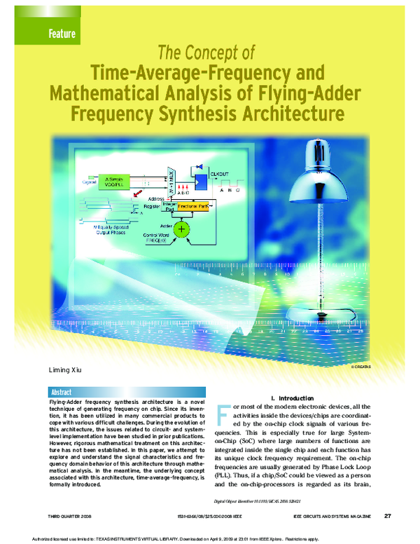
 Liming Xiu