Exploiting STI Stress for Performance
Andrew B. Kahng†‡ , Puneet Sharma‡ , Rasit O. Topaloglu†
and ‡ ECE Departments, University of California at San Diego
Advanced Micro Devices
abk@cs.ucsd.edu, sharma@ucsd.edu, rtopalog@cs.ucsd.edu, rasit.topaloglu@amd.com
† CSE
I. I NTRODUCTION
entire wafer with compressive or tensile liners. Alternatively, dual
stress liners [10], [9] may be used to cover the NMOS devices
with a tensile liner and PMOS devices with a compressive one.
Stress memorization technique [11], [12], used typically to improve
NMOS speed, relies on plastic deformation of certain materials due
to a process step and the consequent memorization of the applied
stress in the channel. Finally, in the hybrid orientation technique
[8], [6], crystal orientations are used to enhance NMOS and PMOS
speeds separately.
STI stress is the stress that is exerted by STI wells on device
active regions and is generally compressive in nature. Irrespective
of the use of stress modulation techniques in the process, STI stress
is not negligible and its magnitude depends on the sizes of the STI
wells and the active regions for a given process. In this paper, we
present a technique that modulates stress at timing critical devices
to improve circuit delay by altering the STI widths (STIW) adjacent
to the devices.
At the 65nm process node and beyond, it is evident that stressand strain-based techniques for mobility improvement will dominate
traditional geometric scaling to maintain Moore’s Law trajectories
for device performance. Enabling progress has been made in the
manufacturing process and TCAD (modeling and simulation) to
support stress. However, stress has not yet been exploited by layout
optimizations to improve design performance. In this work, we
present a new methodology that combines detailed placement and
active-layer fill insertion to exploit shallow-trench isolation (STI)
stress for IC performance improvement. Our methodology begins
with process simulation of a production 65nm STI technology, from
which we generate mobility and delay impact models for STI stress.
We develop STI stress-aware SPICE modeling and simulation of
critical paths, and finally perform timing-driven optimization of STI
stress in standard cell designs, using detailed placement perturbation
to optimize PMOS performance and active-layer fill insertion to
optimize NMOS performance.
Stress Modulation Techniques in the Process.
In 65nm
processes, a number of stress modulation techniques have been
introduced:
SiGe stress from underneath the channel
Embedded SiGe from the source and drain
Stress liner
Stress memorization
Hybrid orientation
Early stress modulation methods employed a Silicon-Germanium
(SiGe) layer underneath the channel, which improves the channel
mobility. More recently, embedded SiGe (e-SiGe) [4], [5], [7] has
been used in the source and drain regions to exert stress along
the channel, and improve PMOS speed. The stress liner technique
involves deposition of stressed liners over the transistors on top
of the polysilicon. Single stress liners may be used to cover the
Stress Modeling Techniques. In the area of stress modeling and
characterization, Rueda et al. [1] have provided general models for
stress. Gallon et al. [16] have specifically analyzed the stress induced
by STI. Bradley et al. [17] have characterized the piezo-resistance
of CMOS transistors. Sheu et al. [22] have modeled well edge
proximity effect on MOSFETs, and [15] have modeled the effect of
mechanical stress on dopant diffusion. Su et al. [18] have proposed a
scalable model for layout dependence of stress. Miyamoto et al. [23]
have provided a layout dependent stress analysis of STI. Recently,
Tsuno et al. [25] have shown that STI width stress effect can impact
drive current by up to 10%.
With respect to the STI process, several optimizations have
been developed to reduce the STI stress, but they typically fail
to completely eliminate layout-dependent stress impacts. Elbel et
al. [13] have proposed an STI process flow based on selective
oxide deposition. Lee et al. [14] have proposed an optimization for
densification of the STI fill oxide to reduce the stress. Miyamoto
et al. [23] also have proposed process innovations to reduce the
active-area layout dependence of MOSFET characteristics. Looking
forward, the introduction of e-SiGe for certain 65nm nodes in the
source and drain may reduce the stress variation due to STIW
for PMOS, but NMOS performance can still be actively improved
by exploiting the STI width effect. If these STI stress controlling
techniques are used, we expect the improvements demonstrated in
this paper to reduce but remain non-negligible.
Stress TCAD simulations have been conducted by Moroz et al.
in [19] and [21], and by Smith in [20]. The work of Moroz et al.
is significant for indicating possible ways to enhance performance
using STI stress; however, no circuit-level optimizations are explained. With respect to the current body of knowledge: (1) models
are still needed to relate stress due to the STI width effect to
transistor mobilities, and (2) there is still a lack of available stress
Abstract— Starting at the 65nm node, stress engineering to improve
performance of transistors has been a major industry focus. An intrinsic
stress source – shallow trench isolation – has not been fully utilized up
to now for circuit performance improvement. In this paper, we present
a new methodology that combines detailed placement and active-layer
fill insertion to exploit STI stress for performance improvement. We
perform process simulation of a production 65nm STI technology to
generate mobility and delay impact models for STI stress. Based on
these models, we are able to perform STI stress-aware delay analysis
of critical paths using SPICE. We then present our timing-driven
optimization of STI stress in standard cell designs, using detailed
placement perturbation to optimize PMOS performance and activelayer fill insertion to optimize NMOS performance. We assess our
optimization on small designs implemented with a 65nm production
cell library and a standard synthesis, place and route flow. Our
timing-driven optimization of STI stress impacts can improve clock
frequency by between 7% to 11%. The frequency improvement through
exploitation of STI stress comes at practically zero cost in terms of
design area and wirelength.
✁
✁
✁
✁
✁
1-4244-1382-6/07/$25.00 ©2007 IEEE
83
�TABLE I
I MPACT OF PLACEMENT ON STI WIDTH AND CONSEQUENTLY ON
RISE (R-Delay) AND FALL (F-Delay) DELAYS FOR A FEW CELLS .
F OR EACH CELL IN THE TABLE , THREE INSTANCES OF IT ARE
PLACED WITH DIFFERENT SPACINGS BETWEEN THEM , AND THE
DELAY OF THE CENTER INSTANCE IS REPORTED . Spacing IS THE
SPACING BETWEEN CELLS . STIW-P (STIW-N) IS THE STI WIDTH
NEXT TO PDIFF (NDIFF) ON BOTH SIDES OF THE CENTER CELL .
Cell
INVD0
BUFFD0
NR2D0
ND2D0
Spacing
(nm)
0um
5um
0um
5um
0um
5um
0um
5um
STIW-P
(nm)
140
5140
140
5140
140
5140
140
5140
STIW-N
(nm)
110
5110
125
5125
110
5110
110
5110
R-Delay
(ps)
24.16
28.05
43.79
46.99
43.58
54.08
25.98
30.49
F-Delay
(ps)
23.51
22.53
43.14
44.85
24.66
23.42
38.19
33.84
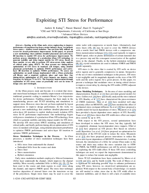
Fig. 1.
Stress components on a unit volume.
II. STI W IDTH S TRESS M ODELING
Based on the understanding in [1], the stress components on a unit
cell are as shown in Figure 1. The stress vector Tx acting normal
to x is given as Tx σxx x̂ σxy ŷ σxz ẑ. The stress tensor is
defined by the three stress vectors:
☎
✂
optimization methods. A fundamental research goal is to develop
novel and efficient simulation, modeling, analysis, and optimization
methods to support next-generation stress-aware EDA technology.
Our work strives to enable this.
☎
✄
✄
✄
✆✝
σi j
Our Focus: Exploitation of STI Width Effect.
STI is an
important and well-studied stress source that has not been fully
exploited until now for design quality improvement. STI usually
exerts a compressive stress along the channel (i.e., the current flow
direction), which improves PMOS device mobility. The opposite
type of stress, tensile stress, degrades the PMOS performance in this
direction. NMOS is in general complementary to PMOS in terms
of how it is affected by stress, and its mobility degrades because of
STI stress.
✂
✞✟
σxx
τyz
τzx
τxy
σyy
τzy
τxz
τyz
σzz
In this equation, σii ’s are stress components normal to the unit
cube faces, whereas τi j ’s are shear components directed towards j
on the orthogonal face to i. The σii ’s are used for analyzing the
impact of stress. Using the individual stress components, we may
convert the stress values to mobility [21].
orthogonal
parallel
W
Device mobility increase corresponds to speed increase. Hence,
it is possible to utilize STI, which is used to separate NMOS and
PMOS regions, to improve performance. Table I shows the impact
of STIW on rise and fall delays (averaged over all timing arcs)
of several 65nm standard cells using the models developed in this
paper. It is possible to both speed up and slow down cells by
controlling the STIW and, thereby, the stress that is applied to
a cell. In particular, larger STI width will generate more stress
in neighboring transistors. In this paper, we propose placement
perturbation and the insertion of active-layer fills to control the STI
width in a performance-driven manner.
STIW
STIW
LOD
STIW parameter. LOD is accounted for in BSIM models.
STIW impact is not modeled. Parallel and orthogonal distances with
respect to a transistor are also indicated in the figure.
Fig. 2.
The remainder of this section describes a generic STI process
flow, along with the STIW models we propose. The STIW parameter
is as shown in Figure 2.
A. Process Steps
The proposed active-layer fill insertion and placement perturbation do not require additional process steps or add complications to
resolution enhancement techniques. Active-layer fill insertion is a
standard process step that is performed in all designs to control
active layer density. Placement perturbation yields a new legal
placement. We ensure that the design is design rule correct after
we perform these two steps.
The process recipe that we use for simulation of STI stress is
summarized in Table II. We have simulated the structure up to the
gate deposition step using the Synopsys Sentaurus 2005.12 process
simulator.1
We make the following observations.
We use a high mesh density, especially between the STI
and underneath the channel, to obtain accurate finite-element
calculations close to the channel.
Temperature cycling during the densification step, i.e., Steps
9 to 11, is responsible for thermal mismatches. Most of the
simulated stress can be attributed to the thermal mismatch.
✁
Organization of the Paper.
The remainder of this paper is
organized as follows. In the next section, we describe our STI widthinduced stress models that we have developed. After a brief introduction to stress, we review the process steps we have simulated using TCAD tools, and our proposed stress models. In Section III, we
present our STI stress-aware timing analysis approach. Section IV
describes our timing optimization methodology. In Section V, we
present our circuit-level optimization results. Section VI concludes.
✁
1
When foundry models are used, the exact process steps are not known
except for hints provided in the literature or various collateral documentation.
Foundries should provide STI width impact models in such a scenario.
84
�TABLE II
In Equation (2), MOB is the mobility multiplier and can be
implemented as described in [24]. Parameters L and R indicate
left and right directions with respect to the channel. The equation
indicates that to find the final mobility, mobility multipliers from
the left and right directions of a device should be multiplied. This
final multiplier should furthermore be saturated to ✒ 60%, as values
outside this range would not be physical. The corresponding parameters of the model are given in Table III. The model dependencies
are plotted in Figures 3 and 4 for PMOS and NMOS, respectively.
Note that increasing STIW or decreasing LOD increases PMOS
mobility, whereas decreasing STIW or increasing LOD increases
NMOS mobility.
The ζ factor in Equation (1) comes from mobility normalization.
When models are being generated, assuming that device modeling
test structures with worst-case corners for STI width are present, the
slow N - slow P corner would correspond to data from test structures
with large STI widths near NMOS modeling devices, and/or test
structures with minimum STI widths near PMOS devices. The ζ
parameter should also be set to 1 for PMOS if it is known that
the modeling test structures have maximum STI widths near PMOS
devices. Alternatively, if the STI width is also known to be minimum
for NMOS modeling test structures, the NMOS ζ factor should be
found through normalization.
STI P ROCESS S TEPS
1. Deposit pad oxide
2. Deposit pad nitride
3. Deposit photoresist for STI lithography
4. Anisotropically etch nitride and oxide
5. Strip photoresist
6. Directional etch at a rate of 0.01 for 40 seconds at 86o angle
7. Deposit TEOS oxide at a rate of 1.0 for 0.2 seconds
8. Deposit trench fill oxide
9. Temperature ramp up from 600o C to 1000o C at a rate of
50o C ✠ min
10. Hold temperature for 1 minute at 1000o C
11. Temperature ramp down from 1000o C to 600o C at a rate of
50o C ✠ min
12. Diffuse oxide
13. STI CMP
14. Etch nitride isotropically at a rate of 0.15 for 1.5 minutes
15. Etch oxide isotropically at a rate of 0.02 for 1 minute
16. Temperature ramp up from 600o C to 800o C at a rate of
40o C ✠ min
17. Diffuse for 5 minutes using dry O2
18. Temperature ramp down from 800o C to 600o C at a rate of
40o C ✠ min
19. Deposit polysilicon gate
✁
In Step 13, STI CMP is applied. At the end of this step, the
top of the STI is left above the active region on purpose. The
basic reason is to avoid defectivity such as delamination of
the STI oxide. At the edges of the channel, this step height
difference would introduce threshold voltage variations and socalled “width effects.”
TABLE III
M ODEL PARAMETER TABLE
ζ
1
1.3333
NMOS
PMOS
α
0.1102
-0.0859
β
0.0729
-0.0450
B. STI Stress Modeling
The popularly used BSIM SPICE model (revision 4.3 and higher)
contains an explicit STI model. However, only the impact of the
distance from transistor channel to the STI boundary is modeled.
Hence, the dependency on the STI width is not present in the BSIM4
model. Our simulations, as well as simulations and data in the
literature, show that STIW impact cannot be neglected. Thus, as
noted above, our present work not only models STIW impact, but
also builds upon this modeling to improve circuit performance at
no area cost.
The STI impact as a function of length of diffusion (LOD)
(refer to Figure 2) is already incorporated into the BSIM4 model.
Our objective is to isolate and correct for the impact of STIW,
in a manner that can be applied on top of existing BSIM4 stress
modeling. Using 2D simulations, we have developed the model
given in Equation (1) to capture the STIW effect in the parallel
direction. The LOD parameter still appears in the equation, as the
STIW impact differs according to the choice of LOD. Also, for
purposes of this paper, we do not require or discuss STIW impact
modeling in the orthogonal direction, as the STI width effects are
blocked in the orthogonal directions by active regions for the type
of standard cells we have used. At the end of TCAD simulations,
we obtain stress values in Pascals. We then convert the stress
values to mobilities using the methodology in [2] and normalize
the mobilities. The mobility equations are given as:
MOBL ✡ R
✂
ζ ☛✌☞ LOD ✍ 2 ✎
α
☎
β ✍ ST IWL ✡ R ✏
MOB ✂ MOBL ✑ MOBR
1.2
STIW=2um
STIW=1um
STIW=0.5um
STIW=0.2um
1.1
MOB
1
0.9
0.8
0.7
0
2
4
6
LOD (um)
8
10
PMOS Dependency on STI Width in Parallel Direction.
Increasing STIW or decreasing LOD increases PMOS mobility.
Fig. 3.
Analyses and optimizations proposed in the rest of the paper are
not tethered to the models developed in this section, and can be used
with other models after appropriate modifications. For example,
there are known STI processes which may induce tensile instead
of compressive stress. This may be due to STI trench height, or
material and thermal processing differences, such as HDP (High
Density Plasma) CVD (Chemical Vapor Deposition) as used in [3].
The optimization procedure presented below can be adopted to such
a scenario with minor changes. Furthermore, the proposed models
show monotonic response with respect to the STI proximity and
widths. This results in an optimization scheme where maximum
or minimum allowed dimensions will improve performance. With
models that are non-monotonic, the optimization algorithm would
need to be altered to provide an optimal solution.
(1)
(2)
85
�Cell-level netlists which describe the connectivity of the devices that comprise individual cells. Cell-level netlists instantiate device-level models and allow SPICE to simulate
waveforms at the outputs of cells in the library when subjected
to a stimuli.
Critical path netlists which describe the connectivity between
the cells for each critical path. Critical path netlists instantiate
cell-level netlists and can be simulated to calculate the delay
of the critical paths.
As noted above stress-induced device mobility change is determined by: (1) the separation between the gate and the active edges,
and (2) by the size of the STI region that surrounds the active region
of the device. Fortunately, the separation between gate and active
edges is fixed when the cells are designed, and the contribution of
this separation to stress and mobility can be modeled at the cell
level. Specifically, in the BSIM 4.3.0 device-level models, stress
parameters SA, SB, and SC have been introduced to model the
stress effect as a function of gate and active edge separation. In
cell-level netlists these parameters are passed with the instantiation
of the device-level models. Cell-level netlists are used in library
characterization to generate gate-level timing models for use in STA.
An example of device-level instantiation with stress parameters is
shown in Figure 5.
1.5
✁
1.4
MOB
1.3
1.2
1.1
✁
1
STIW=2um
STIW=1um
STIW=0.5um
STIW=0.2um
0.9
0.8
0
2
4
6
LOD (um)
8
10
NMOS Dependency on STI Width in Parallel Direction.
Decreasing STIW or increasing LOD increases NMOS mobility.
Fig. 4.
Even as new mobility enhancement techniques show substantial
variation in mobility, STI has been a mainstream methodology
for over a decade. STI processes are much better controlled than
the new stress engineering methods. Hence, there is much smaller
observed variability in the STI mobility impact. Lithography effects
will show negligible impact on the mobility change due to STI, as
long as the layout is designed considering DFM rules such as using
regular active regions without unnecessary corners.
Finally, since active-layer fill insertion is a knob that we propose
to exploit, we comment on additional process considerations for
active-layer filling.
There exist design rules which restrict the maximum active
layer density, with this constraint arising for reasons of STI
CMP uniformity. Such rules must be observed.
Insertion of active-layer fills can potentially increase the total
capacitance of inter-cell M1 routing, and may induce additional
RCX modeling and characterization for a given process technology. However, our methodology should not affect extraction
of intra-cell M1 routing; as our active-layer fills are floating,
their impact is smaller.
Reduced STI widths may slightly increase leakage between
NMOS and PMOS transistors as well as between devices of
the same type. However, the active to active design rules are
set such that the leakage is minimized to a negligible level.
.subckt INVX1 A Z
MM1 D G S B NCH SA=0.2u SB=0.2
MM2 D G S B PCH SA=0.19u SB=0.19u
✁
.ends
✁
.model NCH NMOS (
*Other stress parameters defined
)
Instantiation of device-level models in a standard cell SPICE
netlist. The parameters added in BSIM 4.3.0 to partially model stress
are shown in bold.
Fig. 5.
✁
The stress effect due to STI width is not modeled primarily for
the following two reasons:
STI width is determined by the placement of the cells, so
that stress effect due to STI cannot be captured in library
characterization. A new methodology that analyzes a placed
design and annotates STI width information for use in timing
analysis is required.
Stress effect due to STI is of smaller magnitude than gate and
active edge separation.
III. S TRESS -AWARE T IMING A NALYSIS
In this section we describe our STI stress-aware timing analysis
methodology. We adapt the traditional SPICE-based timing analysis
flow to consider stress induced by STI widths.
✁
A. Traditional SPICE-Based Timing Analysis
Cell-level static timing analysis tools such as PrimeTime offer a
good tradeoff between accuracy and analysis speed. Full designs or
their blocks are typically analyzed and signed off with circuit-level
static timing analysis (STA). However, if greater accuracy is desired,
SPICE-based analysis, which has better accuracy but substantially
slower analysis speed, is employed. Since running full-chip SPICE
analysis is not feasible, critical paths are first identified with static
timing analysis and then simulated with SPICE.
A typical netlist input to SPICE is layered into the following
three tiers:
Device-level models which contain transistor parameters in the
form of coefficients of functions defined in BSIM or equivalent formats. Device-level models allow output waveforms for
PMOS and NMOS devices to be simulated.
✁
B. STI Stress-Aware Timing Analysis
Our approach analyzes the placement of a design and the standard
cell layouts to calculate the STI widths for all critical cells in the
design. The STI widths are then passed as parameters which are
used in the models developed in the previous section.
We modify the cell-level netlists such that parameters
PL PR NL NR which capture the STI width are passed to them.
Parameter PL is the spacing between the boundary of a cell and the
neighboring active region to the left of its positive active region.
Similarly parameter PR is the spacing between the boundary of a
cell and the neighboring active region to the right of its positive
✓
✁
86
✓
✓
�mobility. In our analysis and optimization, we focus on the cells
with simple active shapes and do not change the mobilities for
cells with complex active shapes (i.e., use traditional analysis and
no optimization for them). Fortunately, the most frequently cells
such as inverters, buffers, NAND’s, NOR’s, AND’s, and OR’s have
simple active shapes so we consider and optimize most cells in our
designs.
active region (PRX). Parameters NL, and NR are similarly defined
for negative active regions (NRX). The parameters are set in the
critical path netlists when cells are instantiated as shown in the
example in Figure 6.
* Critical path 00001
X01 N1 N2 INVX1 PL=0.08u PR=4.08u NL=0.06u NR=4.06u
X02 N2 1 N2 NAND2X1 PL=5.0u PR=5.0u NL=5.0u NR=5.0u
C. Alternative Flow
X03 N3 N4 BUFFX1 PL=2.1u PR=5.0u NL=2.04u NR=5.0u
STI stress aware timing analysis can also be performed by
cell-level STA. Towards this standard cells in the library can be
characterized for different STI width configurations around them.
For each standard cell, variants may be created corresponding
to each STI width configuration. Given the STI width, models
presented in the previous section are used in library characterization.
The STI width of a cell in a design can be computed from the
placement and standard cells layouts, and can be used to find the
variant that has the closest STI width configuration. The cell can
then be bound to the variant in the library and cell-level STA run
to perform STI stress aware timing analysis.
.subckt INVX1 A Z
.param PMOB = Our_PMOS_Model (PL, PR, NL, NR)
.param NMOB = Our_NMOS_Model (PL, PR, NL, NR)
MM1 D G S B NCH SA=0.2u SB=0.2 MOB=NMOB
MM2 D G S B PCH SA=0.19u SB=0.19u MOB=PMOB
.ends
.model NCH NMOS (
*Other stress parameters defined
IV. T IMING O PTIMIZATION
In this section we present our timing optimization methodology.
The basic idea exploited in our optimization is that STI widths
of devices can be altered to change their mobility and improve
performance. Specifically, the alteration involves increasing the STI
widths for PMOS devices and decreasing them for NMOS devices.
We identify the timing critical cells and alter their STI widths
to improve the circuit performance. In our approach we use the
following two knobs to alter the STI widths:
Placement perturbation. The placement of a layout can be
changed to increase or decrease the spacing between neighboring cells which directly increases or decreases the STI width.
Additionally, spacing cells apart can allow fills, for which
initially there was insufficient space, to be inserted.
Active layer fill (RX fill) insertion. Active layer fills are
rectangular dummy geometries inserted on the active (RX)
layer primarily to improve planarity after chemical mechanical
polishing (CMP). However, such geometries also reduce the
STI width of the devices next to which they are inserted. The
STI width after insertion of an RX fill next to a device is the
spacing between the active region of the device and the fill.
We now present the details of the above two knobs.
)
Fig. 6. Critical paths instantiate cell-level netlists which instantiate
device-level models. Our modifications to the traditional flow to model
STI width dependent stress are shown in bold.
The PL PR NL NR parameters can be calculated from the placement and the cell’s layouts, specifically, the cell boundary to active
spacings. Computation of PL for a cell, which is the spacing
between the cell’s boundary and the positive active region of the
cell to its left, is as follows. The spacing between the cell and its left
neighboring cell is found from the placement. The spacing between
the positive active region of the neighbor and its cell boundary is
found from layout analysis of the neighbor. The two spacings are
then added, with correct consideration of the orientations of the cell
and its neighbor. Other parameters PR, NL, and NR are calculated
similarly. Figure 7 illustrates the calculation.
✓
✓
✓
Neighbor L
W
X
Cell B
Y
PL
PR
NL
NR
PL = W + X
✁
✁
Neighbor R
Z
A. Active Layer (RX) Fill Insertion
Even though RX fills are non-functional geometries, their effect
on the stress is identical to that of active regions of devices.
When inserted next to the active region of an NMOS device, fills
substantially reduce the STI width and stress of the device, and
consequently improve the performance of the NMOS device. On
the other hand, fills inserted next to a PMOS device reduce STI
width and stress but consequently degrade the performance. Hence,
inserting fill next to the NMOS devices but not next to the PMOS
devices of a cell improves performance.
Circuit delay improves when the delay of setup-critical cells is
reduced. So, we insert rectangular RX fills next to the NMOS
devices, to the left and right of the cell. No RX fills are inserted
next to the PMOS devices; so the PMOS remains exposed to a
large STI width and stress. The devices closer to the active boundary
experience the maximum benefit of this optimization. Since the most
PR = Y + Z
Fig. 7. Calculation of parameters PL, PR, NL, and NR from inter-cell
spacings and active to cell boundary spacings.
We note that our flow needs modifications to work for cells
with complex active shapes such as flip-flops and multiplexors.
Active shape complexities include non-rectangular shapes and noncontinuous shapes. To model STI stress impact for non-rectangular
active shapes, modifications such as those employed by BSIM to
handle non-rectangular active may be used. For cells with noncontinuous active shapes, devices can be completely shielded from
STI width outside the cell and our flow should not alter their
87
�frequently used cells in the designs are small, a large fraction of
devices in the design benefit from fill insertion. Our technique can
also be employed for hold-time critical cells in the reverse manner,
i.e., insert fills next to the PMOS devices but not next to NMOS
devices to slow down the cell.
Figure 8 shows an example standard cell with PRX (active regions
for PMOS devices) and NRX (active regions for NMOS devices).
As can be seen, active regions exist under the top and bottom cell
boundary that completely shield the cell from STI stress effects
in the direction orthogonal to the carrier (current) flow direction.
Hence, we only apply our optimization in the parallel direction by
inserting fill to the right and left of a cell. Figure 9 illustrates fill
insertion for hold- and setup-critical cells. For a hold-critical cell,
PRX fills are inserted next to the PRX region to reduce stress and
slow down the PMOS devices. For a setup-critical cell, on the other
hand, NRX fills are inserted next to the NRX region to reduce stress
and fasten the NMOS devices.
B. Intra-Row Placement Optimization
We now present the placement perturbation knob which can
increase (decrease) the STI width and improve PMOS (NMOS)
performance. Placement of a cell determines its location (consequently its neighbors and spacings with them) and its orientation.
In our optimization we change the locations of the cells such that
spacings are altered but the ordering of cells in a standard cell
row is not affected. Increased spacing next to a cell, increases the
STI width and improves the delay of the PMOS devices. However,
the delay of the NMOS devices increases with increased spacing.
Fortunately, we can utilize our first knob, RX fill insertion, to reduce
the NMOS STI width and improve its delay as well. In fact, if the
spacing between cells is too small for fill insertion, placement can
facilitate fill to be inserted by creating additional space for it.
For a setup-critical cell, we perturb the placement to increase
the spacing on both sides of the cell. The placement perturbation
just reorganizes the whitespace in the standard cell row of the
cell without requiring any additional space. Then we insert RX fill
on both sides of the NMOS active (NRX). For hold-critical cells,
spacing can be first increased using placement perturbation and fills
inserted next to the PMOS active (PRX).2
Minimizing Timing Impact. The perturbation of detailed placement from the original placement results in wirelength change,
which can impact wire parasitics and consequently timing. Even
though our localized placement perturbations do not significantly
affect timing, small changes in the timing of critical paths can affect
the minimum clock cycle time. To minimize the timing change
of critical paths, we fix the cells and nets in the critical paths.
Fixed cells are not moved during optimization and fixed nets are
not changed during engineering change order (ECO) routing that
is performed after optimization. Since the nets in the critical path
are fixed, all cells connected to these nets should also be marked
as fixed and not moved during optimization. We note that the delay
of such nets can marginally change due to the coupling capacitance
with neighboring nets, the routing for which may change. We also
fix all flip-flops, clock buffers, and clock nets to avoid any impact
on the clock tree.
Our intra-row placement optimization attempts to create space
on the right and left sides of each timing critical cell such that
the STI width of the cell exceeds ST IW sat which is the STI width
at which stress saturates. Space larger than ST IW sat affects stress
negligibly as can be seen in Figures 3 and 4; from the figures we
set ST IW sat to 2µm. In the process, the minimum number of cells
are displaced to minimize the wirelength impact. ST IW sat is always
greater than the space required to insert RX fill so if the placement
perturbation is able to create a space greater ST IW sat , fill can be
inserted where needed. Due to the presence of other timing critical
cells and “dont-touch” cells, placement perturbation is not always
able to create a space greater than ST IW sat . Figure 11 demonstrates
placement perturbation and fill insertion for setup-time optimization
on a standard cell row.
While it is possible to perform fill insertion without placement
perturbation, we have found the associated performance benefits
to be very small. Both knobs complement each other: placement
creates space for fill insertion and fill insertion improves the perfor-
PRX
Cell
Boundary
NRX
Fig. 8. A generic standard cell with polysilicon, positive active regions
(PRX), negative active regions (NRX), and cell boundary shown.
PRX FILL
PRX FILL
NRX FILL
Hold Critical
NRX FILL
Setup Critical
The generic cell of Figure 8 optimized with fill insertion for
hold-time and setup-time criticality.
Fig. 9.
Figure 10 illustrates the approach for a few setup-critical cells in
a standard cell row.
✚✕✙✚✕✙✚✕✙ A✚✕✙✚✕✙✚✕✙ ✚✙✚✙✚✙
✚✙✕✚✙✕✚✙✕✚✕✙✚✕✙✚✕✙ ✚✙✚✙✚✙
✚✙✕✚✕✙ ✚✕✙✚✕✙ ✚✙✚✙
B
✖✕✔✖✕✔✖✕✔ C✖✔✖✔✖✔
✖✔✕✖✔✕✖✔✕✖✔✖✔✖✔
✖✔✕✖✕✔ ✖✔✖✔
✗✕✗✕✗✕✘✕✗✘✕✗✗ D✘✕✗✘✕✗✗ ✘✗✘✗✗
✗✕✗✕✗✕✘✕✘✕✗✘✕✗✗ ✘✕✘✕✗✘✕✗✗ ✘✘✗✘✗✗
✗✕✗✕✘✕✘✕✗✘✕✗ ✘✕✘✕✗✘✕✗ ✘✘✗✘✗
E
A row of standard cells after active layer fill insertion for
setup-time improvement. Cells patterned with diagonal lines are the
setup-critical cells and filled rectangles are the inserted active layer fills.
Fig. 10.
All fills are inserted subject to the design rule constraints (DRCs)
and introduce no DRC violations. We have already noted that no
additional mask step is required, and that M1 capacitance impact
is likely negligible. Since the fill insertion knob can only decrease
STI width, NMOS performance can be improved but PMOS performance can at best be kept constant. However, neighboring cells
which have very small spacing and between which fills cannot be
inserted can be spaced apart by placement perturbation to allow fills
to be inserted.
2 When both hold- and setup-critical cells are optimized, the following
corner case arises. If intra-row neighboring are hold- and setup-critical, their
optimizations are conflicting to each other. Hence, the spacing between them
is divided in half and alternating PRX and NRX fills inserted.
88
�✰✕✰✕✱✕✰✰ A✱✕✰✰ ✱✰✰
✰✕✰✕✱✕✱✕✰✰ ✱✕✱✕✰✰ ✱✱✰✰
✱✕✱✕✱
✯✕✮✯✕✮✯✕✮ B✯✕✮✯✕✮✯✕✮ ✯✮✯✮✯✮
✯✮✕✯✯✮✮✕✕✯✕✮✯✕✯✕✮✮ ✯✮✯✯✮✮
✯✮✕✯✕✮ ✯✕✮✯✕✮ ✯✮✯✮
C
D
✬✕✬✕✬✕✭✕✬✭✕✬✬ E✭✕✬✭✕✬✬ ✭✬✭✬✬
✬✕✬✬✕✕✭✕✭✕✬✭✕✬✬ ✭✕✭✕✬✭✕✬✬ ✭✭✬✭✬✬
✬✕✬✕✭✕✭✕✬✭✕✬ ✭✕✭✕✬✭✕✬ ✭✭✬✭✬
F
Input: Placed design; set of timing critical cells, T ; set of
“dont-touch” cells, D; STI width beyond which stress saturates,
ST IW sat
Output: New placement with altered inter-cell spacings
Before Optimization
✤✕✤✕✥✕✤✤ A✥✕✤✤ ✥✤✤
✤✕✤✕✥✕✥✕✤✤ ✥✕✥✕✤✤ ✥✥✤✤
✥✕✥✕✥
✣✕✣✕✢✢✣✕✢ B✣✕✣✕✢✢✣✕✢ ✣✣✢✢✣✢
✣✢✕✣✢✕✣✢✕✣✕✢✣✕✢✣✕✢ ✣✢✣✢✣✢
✣✢✕✣✕✢ ✣✕✢✣✕✢ ✣✢✣✢
sat
STIW
C
sat
D STIW
E
✛✕✛✕✛✕✜✕✜✕✛✛✛ ✜✕✜✕✛✛✛ ✜✜✛✛✛
✛✕✛✕✛✕✜✕✜✕✛✜✕✛✛ ✜✕✜✕✛✜✕✛✛ ✜✜✛✜✛✛
✛✕✛✕✜✕✜✕✛✜✕✛ ✜✕✜✕✛✜✕✛ ✜✜✛✜✛
sat
STIW
F
1
1.1
1.2
createRightSpace(t)
1
n = cellsToMoveRight(t);
2
moveCellsRight(t, n);
After Placement Perturbation
✪✕✪✕✫✕✪✪ A✫✕✪✪ ✫✪✪
✪✕✪✕✫✕✫✕✪✪ ✫✕✫✕✪✪ ✫✫✪✪
✫✕✫✕✫
✩✕★✩✕✩✕★★ B✩✕★✩✕✩✕★★ ✩★✩✩★★
✩★✕✩★✕✩★✕✩✕★✩✕★✩✕★ ✩★✩★✩★
✩✩✕★★✕✩✕★✩✕★ ✩✩★★
C
D
✦✕✦✕✦✕✧✕✦✧✕✦✦ E✧✕✦✧✕✦✦ ✧✦✧✦✦
✦✕✦✕✦✕✧✕✧✕✦✧✕✦✦ ✧✕✧✕✦✧✕✦✦ ✧✧✦✧✦✦
✦✦✕✕✧✕✧✕✦✧✕✦ ✧✕✧✕✦✧✕✦ ✧✧✧✦✦
forall cells t ✲ T
createRightSpace(t)
createLeftSpace(t)
F
cellsToMoveRight(t)
1
i ✳ t;
2
j ✳ cellToRightOf(t);
3
accumulatedSpacing = 0;
4
cellsToMove = 0;
5
while accumulatedSpacing ✴ ST IW sat and j ✲ ✵ D
5.1
accumulatedSpacing += interCellSpacing(i, j);
5.2
cellsToMove++;
5.3
i✳ j
5.4
j ✳ cellToRightOf(i);
6
return cellsToMove;
After Placement and Fill Optimization
Fig. 11. Placement change and fill insertion for setup-time optimization.
A standard cell row is shown before optimization, after placement
perturbation, and after fill insertion. ST IW sat is the STI width beyond
which stress effect saturates. Cells pattered by diagonal lines are the
setup-critical cells for which timing is optimized. “Dont-touch” cells are
pattered with the brick pattern and their placement cannot be changed.
moveCellsRight(t, n)
1
// flushes n cells to the right of Cell t towards the right
mance of the NMOS devices that are slowed down by placement
perturbation.
Figure 12 presents the pseudo-code for our intra-row placement
optimization. For each timing critical cell, right and left spacings
are increased by functions createRightSpace and createLeftSpace
respectively. For the right side, the function cellsToMoveRight finds
the minimum number of cells to move to attain a spacing of
ST IW sat . Then the function moveCellsRight flushes the computed
number of cells to the right as much as possible.
Our overall STI stress-aware placement and fill optimization flow
is as follows:
1) Identify critical paths and critical cells
2) Perform intra-row placement optimization
3) Perform ECO routing followed by parasitic extraction
4) Perform RX fill insertion
5) Evaluate the optimized layout with STI stress-aware timing
analysis
createLeftSpace(t)
1
// similar to createRightSpace(t)
Fig. 12.
Pseudo-code for intra-row placement optimization.
TABLE IV
T ESTCASES USED IN EXPERIMENTAL VALIDATION . MCT IS THE
MINIMUM CYCLE TIME .
Circuit
C5315
ALU
s38417
AES
Source
ISCAS’85
opencores.org
ISCAS’85
opencores.org
#cells
1,408
11,106
8,514
21,000
Utilization
82%
78%
79%
78%
MCT (ns)
0.912
4.333
3.086
4.738
paths delay (TPD), which is the sum of the delays of top critical
paths. While MCT determines the maximum speed at which the
circuits can be run, TPD determines the robustness to variations.
The proposed approach optimizes the delay of several top critical
paths and hence improves the TPD. We also study the affect of our
optimization on wirelength.
Table V presents our results for four testcases. For the testcases
ALU and AES, the optimization improves the MCT and TPD by ✶
10% while incurring negligible increase in wirelength. The testcase
S38417, however, demonstrates a much smaller improvement. We
attributed this to the fact that S38417 is an artificial testcase with
over 50% of its cells flip-flops. Our optimization does not change
the locations of flip-flops to avoid changes to the clock tree and
hence can perturb the placement of fewer cells. Figure 13 shows the
histograms for the delays of top critical paths of our testcase AES
before and after optimization. As can be seen, the delay distribution
has shifted to the left (lower delay) substantially.
We found negligible improvement in hold slack for our testcases.
This is because stress optimization can only change cell delays by
10%-20% and for hold-critical paths the cell delays are very small.
So the change in the delay of hold-critical paths is insignificant
with our approach and traditional delay introduction methods such
as insertion of delay elements or wire snaking must be used.
V. E XPERIMENTAL S TUDY
We now present our experiments to evaluate the proposed optimization methodology. Our experiments assess the impact of our
optimization on the minimum clock cycle time, delay of top critical
paths, and final routed wirelength.
A. Experimental Setup
The details of the testcases used in our experiments are presented
in Table IV. We use Synopsys Design vW-2004.12.SP3 for synthesis, Cadence SOC Encounter (v5.2) for placement, clock tree
synthesis, routing, and parasitic extraction, Synopsys PrimeTime vW2004.12.SP2 for cell level timing analysis, and Synopsys HSPICE
vY-2006.03 for SPICE simulations. For our experiments, we use the
50 most frequently used cells from high-Vth and nominal-Vth 65nm
high-speed libraries. SPICE device models and cell netlists were
supplied by a foundry. We built our optimizer on top of OpenAccess
API v2.2.4.
B. Experimental Results
We evaluate the proposed placement and fill optimization by
assessing the improvement in minimum cycle time (MCT) and top
89
�TABLE V
T IMING OPTIMIZATION RESULTS WITH PLACEMENT AND FILL INSERTION . MCT IS THE MINIMUM CYCLE TIME . WL IS THE WIRELENGTH .
TPD STANDS FOR TOP PATHS DELAY AND IS THE SUM OF THE DELAYS OF THE TOP 100 CRITICAL PATHS .
Circuit
C5315
ALU
s38417
AES
Original
TPD
(ns)
73.56
401.56
280.69
444.79
MCT
(ns)
0.912
4.333
3.086
4.738
WL
(mm)
17.79
211.1
94.06
385.9
MCT
(ns)
0.844
3.890
3.005
4.206
MCT
Improv. (%)
7.42
10.23
2.60
11.25
20
Number of Paths
15
10
5
3.6
3.8
4.0
4.2
4.4
Path Delay (ns)
4.6
4.8
Fig. 13. Path delay histograms for the top 100 critical paths of testcase
AES before and after optimization.
VI. C ONCLUSIONS
We have conducted TCAD process simulations to generate models that relate the dependence of transistor mobilities to stress
induced by STI width. We have proposed an STI width-aware design
methodology for standard cell place-and-route designs. We have
also devised an optimization methodology, based on cell placement
perturbation, to create extra space around critical cells; this is
followed by dummy diffusion insertion. The proposed optimization
flow, while demonstrated with our models, can be generalized to
other STI stress models. We have applied the proposed optimization
flow on a number of testcases implemented with industry 65nm
libraries. Our data shows that STI width optimization can increase
performance by 7% to 11% with no area penalty. The proposed
optimization can form the basis of circuit optimization that exploits
upcoming stress-engineered transistor technologies in 65nm and
below processes.
VII. ACKNOWLEDGMENTS
We would like to thank Frank Geelhaar of AMD for useful
discussions, and Swamy Muddu for help with the implementation
and the testcases.
R EFERENCES
[1] H.A. Rueda, “Modeling of Mechanical Stress in Silicon Isolation
Technology and Its Influence on Device Characteristics,” Ph.D. Thesis,
1999.
[2] C.S. Smith, “Piezoresistance Effect in Germanium and Silicon,” Physical Review, Vol. 94, No.1, pp. 42-49, 1953.
[3] S.W. Chung et al., “Novel Shallow Trench Isolation Process Using
Flowable Oxide CVD for Sub-100nm DRAM,” Proc. IEDM, pp. 233236, 2002.
[4] J.-P. Han et al., “Novel Enhanced Stressor with Graded Embedded SiGe
Source/Drain for High Performance CMOS Devices,” Proc. IEDM,
2006.
[5] Q. Ouyang et al., “Characteristics of High Performance PFETs with
Embedded SiGe Source/Drain and 100 Channels on 45o Rotated
Wafers,” Int. Symp. On VLSI Technology, pp. 27-28, 2005.
✷
WL
(mm)
17.79
210.9
94.03
385.2
∆WL
(%)
+0.00
-0.09
-0.03
-0.10
[6] Y. Tateshita et al., “High-Performance and Low-Power CMOS Device Technologies Featuring Metal/High-k Gate Stacks with Uniaxial
Strained Silicon Channels on (100) and (110) Substrates,” Proc. IEDM,
2006.
[7] Q. Ouyang et al., “Investigation of CMOS Devices with Embedded
SiGe Source/Drain on Hybrid Orientation Substrates,” Symposium on
VLSI Technology, pp. 28-29, 2005.
[8] M. Yang et al., “Hybrid-Orientation Technology (HOT): Opportunities
and Challenges,” IEEE Tran. On Electron Devices, Vol. 53, No. 5, pp.
965-978, 2006.
[9] W.-H. Lee et al., “High Performance 65 nm SOI Technology with Enhanced Transistor Strain and Advanced-Low-K BEOL,” Proc. IEDM,
2005.
[10] H.S Yang et al., “Dual Stress Liner for High Performance sub-45nm
Gate Length SO1 CMOS Manufacturing,” Proc. IEDM, 2004.
[11] C. Ortolland, “Stress Memorization Technique (SMT) Optimization for
45nm CMOS,” Symp. on VLSI Technology, pp. 78-79, 2006.
[12] C.-H. Chen et al., “Stress Memorization Technique (SMT) by Selectively Strained-Nitride Capping for Sub-65nm High-Performance
Strained-Si Device Application,” Symp. on VLSI Technology, pp. 56-57,
2004.
[13] N. Elbel, Z. Gabric, W. Langheinrich and B. Neureither, “A New STI
Process Based on Selective Oxide Deposition,” Symposium on VLSI
Technology Digest of Technical Papers, pp. 208-209, 1998.
[14] H. S. Lee et al. “An Optimized Densification of the Filled Oxide
for Quarter Micron Shallow Trench Isolation (STI),” Symp. on VLSI
Technology Digest of Technical Papers, pp. 158-159, 1996.
[15] Y.-M. Sheu et al. “Modeling Mechanical Stress Effect on Dopant
Diffusion in Scaled MOSFETs,” IEEE Tran. on Electron Devices, Vol.
52, No. 1, pp. 30-38, Jan. 2005.
[16] C. Gallon et al. “Electrical Analysis of Mechanical Stress Induced by
STI in Short MOSFETs Using Externally Applied Stress,” IEEE Tran.
on Electron Devices, Vol. 51, No. 8, pp. 1254-1261, Aug. 2004.
[17] A.T. Bradley, R. C. Jaeger, J.C. Suhling and K.J. O’Connor, “Piezoresistive Characteristics of Short-Channel MOSFETs on (100) Silicon,”
IEEE Tran. on Electron Devices, Vol. 48, No. 9, pp. 2009-2025, Sep.
2001.
[18] K.-W. Su et al., “A Scaleable Model for STI Mechanical Stress
Effect on Layout Dependence of MOS Electrical Characteristics,” IEEE
Custom Integrated Circuits Conference, pp. 245-248, 2003.
[19] V. Moroz et al., “The Impact of Layout on Stress-Enhanced Transistor
Performance,” Int. Conf. on Simulation of Semiconductor Processes
and Devices, pp. 143-146, 2005.
[20] L. Smith, “TCAD Modeling of Strain-Engineered MOSFETs,” Mater.
Res. Soc. Symp. Proc., vol. 913, 2006.
[21] V. Moroz, L. Smith, X.-W. Lin, D. Pramanik and G. Rollins, “StressAware Design Methodology,” Int. Symposium on Quality Electronic
Design, 2006.
[22] Y.-M. Sheu et al., “Modeling Well Edge Proximity Effect on HighlyScaled MOSFETs,” IEEE Custom Integrated Circuits Conference, pp.
831-834, 2005.
[23] M. Miyamoto, H. Ohta, Y. Kumagai, Y. Sonobe, K. Ishibashi and Y.
Tainaka, “Impact of Reducing STI-Induced Stress on Layout Dependence of MOSFET Characteristics,” IEEE Trans. On Electron Devices
51(3), pp. 440-443, 2004.
[24] D. Pramanik, “Impact of Layout on Variability of Devices for Sub
90nm Technologies,” IEEE Electron Devices Society Santa Clara
Chapter Meeting, 2006.
[25] H. Tsuno et al., “Advanced Analysis and Modeling of MOSFET
Characteristic Fluctuation Caused by Layout Variation,” Symposium
on VLSI Technology, pp. 204-205, 2007.
Before Optimization
After Optimization
0
Placement & Fill Opt
TPD
TPD
(ns)
Improv. (%)
68.17
7.07
363.16
9.56
273.83
2.44
394.18
11.38
✸
90
�
 Puneet Sharma