US011360740B1
( 12 ) Kent
United
States Patent
et al .
( 54 ) SINGLE - STAGE HARDWARE SORTING
BLOCKS AND ASSOCIATED MULTIWAY
MERGE SORTING NETWORKS
( 71 ) Applicant: UNM Rainforest Innovations ,
Albuquerque, NM (US )
( 72 ) Inventors: Robert Bernard Kent , Albuquerque,
NM (US ) ; Marios Stephanou
( 10) Patent No .: US 11,360,740 B1
(45 ) Date of Patent :
Jun . 14 , 2022
(52 ) U.S. CI.
G06F 7/16 ( 2013.01 ) ; G06F 77026
(2013.01 ) ; G06F 7/5443 ( 2013.01 )
( 58 ) Field of Classification Search
CPC
G06F 7/16 ; G06F 7/026
See application file for complete search history.
???
U.S. PATENT DOCUMENTS
Pattichis , Albuquerque, NM (US )
Subject to any disclaimer, the term of this
patent is extended or adjusted under 35
U.S.C. 154 ( b ) by 0 days.
( * ) Notice:
A *
A
B2 *
B1 *
4/1984 Coleman
12/1986 Nelson
10/2007 Adas
12/2019 Ferger
5/2008 Mohamed
G06F 7/026
382/218
G06F 7/22
HO4L 49/30
* cited by examiner
Primary Examiner Chuong D Ngo
Related U.S. Application Data
( 60 ) Provisional application No. 62 / 984,880 , filed on Mar.
4 , 2020 .
G06F 7/16
G06F 7/02
GO6F 7/544
4,441,165
4,628,483
7,281,009
10,523,596
2008/0104374 Al
( 21 ) Appl . No .: 17/190,843
Mar. 3 , 2021
(22) Filed :
( 51 ) Int . Cl .
References Cited
( 56 )
( 2006.01 )
( 2006.01)
( 2006.01 )
(74 ) Attorney, Agent, or Firm — Valauskas Corder LLC
( 57 )
ABSTRACT
A system and methods for designing single -stage hardware
sorting blocks , and further using the single - stage hardware
sorting blocks to reduce the number of stages in multistage
sorting processes , or to define multiway merge sorting
networks.
15 Claims , 40 Drawing Sheets
100
In X input Port Values
160
Comparison Signals Block
120
Create N * { N - 1 }/ 2
input comparison Signals
Output MUX Block
Output MUX Select Line Signals Block
Each Out Y
multiplexer assignment
T
140
For each Qut Y, create N - 1
in X goesto Out Y
multiplexer select line signals
contains
Ninput data values
and ( N - 1 ) multiplexer
select line signals
OutY
Output
Port
Values
�U.S. Patent
Jun . 14 , 2022
Sheet 1 of 40
US 11,360,740 B1
nax
Comparison Block :
One 2 - value
Comparison
Out o
ge 10
Output MUX Block :
2-10-1 per-bit
Multiplexers
PRIOR ART
FIG . 1
100
160
in X input fort Values
Comparison Signals Block
120
Create N {N - 1 }/ 2
Input Comparison Signals
140
Output MUX Block
Output
Each Out y
Values
Output MUX Select Line Signals Block
multiplexer assignment
For each Out Y, create N - 1
in X goesto Out Y
multiplexer select line signals
N input data values
contains
and { N - 1} multiplexer
select line signals
FIG . 2
Port
�U.S. Patent
Jun . 14 , 2022
US 11,360,740 B1
Sheet 2 of 40
module sort 9 values 8 bits
# ( parameter MAX BIT_INDEX
M
w
}
(
input
input
input
input
input
input
input
input
( MAX BIT INDEX
( MAX BITINDEX
( MAX_BIT_INDEX
( MAX_BIT_INDEX
( MAX_BIT_INDEX
( MAX BIT INDEX
( MAX BIT INDEX
[ MAX_BIT_INDEX
:
:
:
:
:
:
:
=
0
0
0
0
0
@
0
:
:
:
:
:
:
:
0)
0)
0)
0)
0)
01
0)
input ( MAX BIT INDEX :=
the max value
output
output
output
output
output
output
output
(
(
(
(
(
(
(
MAX BITINDEX
MAX BIT INDEX
MAX BIT_INDEX
MAX_BIT_INDEX
MAX_BIT_INDEX
MAX BIT INDEX
MAX_BIT_INDEX
output ( MAX_BIT_INDEX
output ( MAX BIT INDEX
the min value
FIG . 3
)
)
)
)
)
1
)
1
In
In
In
In
In
In
In
In
8
7
6
5
4
2
1
1 In 0
Out
Out_7
Out 6
Out
Out4
Out 3
Out 2 ,
: 01 Out
: 01 Out o
�U.S. Patent
200
Jun . 14 , 2022
Sheet 3 of 40
US 11,360,740 B1
Start
WWW
Applying to input ports a list of N
unsorted data input values
202
Using a comparison operator to
generate result signals
204
Enforcing an order
206
Providing a set of output
multiplexers
208
Assigning, in parallel, each N data
input value to an output port
210
Outputting to output ports a sorted
list of values
212
Stop
FIG . 4
�U.S. Patent
Jun . 14 , 2022
Sheet 4 of 40
9
// The comparison signals ; " ge " for " >
1 / 36 comparisons for 9 - sorter
wire ge_8_7 ( In 8 > * In 7 ) ;
wire
ge_8.5
wire
ge 83 ( In 8
ge8 2 = ( In8
ge_81 ( In 8
( In8
wire
Wire
wire
wire
( In 8 ** In 5 )
W
M
WY
?==
**
>=
>
)
In 3
In2
In 1
In 0
WY
13
) ;
) ;
) ;
)
1128 comparisons for & Sorter
wire
wire
wire
wire
wire
11 21
wire
wire
Wire
wire
wire
ge 7 6
W
( In 7 > In 6 ) ;
M
sete
ge_73 ( In 7
ge 7 2 * ( In 7
ge 7 1 = ( In 7
ge 7 8 = ( In 7
comparisons for
ge_6 5 = ( In 6
ge_6 4 = ( In 6
ge 6_3 = ( In6
ge 6_2 ( In 6
ge 61 ( In 6
tetek
)
>
>
>=
In 3 ) ;
In 2 ) ;
In 1 ) ;
In ) ;
>
>
>*
>*
In 5
In 4
In3
In 2
In 1
topp
)
)
)
)
)
;
;
;
;
1/15 comparisons for : 6 - sorter
Wire
wire
wire
Wire
wire
ge_53
( In 5
In
w
AN
// 10 comparisons for 5 - sorter
Wire ge_43 * ( In 4 * In 3
wire de 4.2 * ( In 4 * In 2
Wire
wire ge 40 * ( In 4 * In
16 comparisons for 4- sorter
Wire ge3
( In 3 * In 2
wire ge 37 * ( In 3 » In 1
w
M
Wire
) ;
ge 30
( In 3
In
) ;
) ;
)
)
)
)
3 comparisons for 3 - sorter
What mere
ge_2 1 ( In 2 » In 1 )
ge_2_0 = ( In_2 > = In )
1 comparison
Sorten
Wire
ge 10 * ( In 1 > In
A
::
FIG . 5
US 11,360,740 B1
greater than or equal "
�U.S. Patent
Jun . 14 , 2022
assign Out2
( In 8 goes
( In 7 goes
( In6goes
( Ingoes
w
Sheet 5 of 40
to Out 2 ? In 8 :
to out.2 . In :
w
w
w
to Out2 ? In6 :
to out 2 In 5 :
( In 4goes to Out 2. In
In 3.goes_to_out_2 In
( In 2 goes to Out 2 ? In
In goes_to_out_2 In
1
w
US 11,360,740 B1
WY
4
3
2
2
:
:
:
: In_ ) ) ) ) ) ) ) ) ;
FIG . 6
�U.S. Patent
Jun . 14 , 2022
US 11,360,740 B1
Sheet 6 of 40
Start
300
w
Creating for each N data input all
2N -1 possible product terms
302
Select product term
303
Is data input
on left side of operator
AND signal state is non
YES
inverted ?
304
NO
Assign a "win
308
YES
is data input
on right side of operator
AND signal state is
inverted ?
306
NO
Is this the last
comparison signal state
in the product term ?
309
YES
Sum the " wins "
310
Adding to SOP equation
312
Stop
Determine output port assignment
314
FIG . 7
NO
�U.S. Patent
Jun . 14 , 2022
US 11,360,740 B1
Sheet 7 of 40
In_Succes_to_out_5 * xy S & product terms
wire
988..Sealine
?
?
?
66.8.5
?
68
ges
88
The
&&
ge 5..5
BB
&&
ga ... S &&
88
ge5 88
ses
ges
origem
seis Sock …………
&&
8
Big
age 85 8 %
ge 85 &
{
28 get 5
Be
* Le
4
se 5 && ges3
5 4 ods generalde
&
88
( !
ges
g
5 88
? : ? ?.75
&
88
$
ge 7
&&
????
B3 && ! ge2 Suite
?? }
ges
S3 && se 5.2 SS ! Be S.2. S & ge
}
265:58
$ & 5.
&& 26.5.2 LE
ge
88
g
26 5 3
}
I go 50 )
&&
se 5.2 ben
86 ge4
&&&&& ges S & ge 54
&& be
&& gens && ! B. && SS3 &&
8 & ge_7_5 88ge 5.5 : S & g 48 gen ?
} geo &&
}
2 Set 825,2 Led
geS3 && get &&
:1
}
SS.SS PRES
geri Segers 4
ge
a ! ?????
se 5.2
ge65 : Se
& Q 6.5 S &
88
ge * &&
ge4
de 7 && gens && ! Se
se
ge 7.5 88 ge5884 &
SS
ge4 82
ge7 88
ge
Se..9..2 Broase
&
get to see the
80 65 od
tewme els
& SE
&&&&& geboren &&
se 5.2
845 88 gege
)
X2
seu &&
{
!
Be ... Sirge
Seele
&& { ge75 &&
Sige
(
ses So
se & 5 8882558&
ge55 &&
8.35 88
{
??
& !
ge: 7.5 && SE 6.5 Si
g
& t ge5 So home
88
?
se 5.2 Set
gens Bosses &&
get 3 && ! se S..2
FIG . 8
??
gemeente
se 5.2
se$ }
.
iii
�U.S. Patent
Jun . 14 , 2022
module sort.values & bits
#sorameter
{
US 11,360,740 B1
Sheet 8 of 40
MAX 817INDEX
input ( MAX BIT_INDEX : 1 in
1:17
input ( MAX_BIT_INDEX ; 01 190
input ( MAX_BIT_INDEX :
At the sax value
output ( MAX BIT INDEX ; 8 1 Out
output ( MAX_BIT_INDEX ; 61 : Out..
output ( MAX BIT INDEX : 0 ) Out
the min value
The comparison signals
// 3 comparisons for 3 - sorter
wire
In
Wire
*
// 1 comparison for 2 - sorter
Wire
wyn
YAWAVAWAW
MYA
1 / Insoes to out $ 34 ] tiplexer select line signals
niyaya
VANYAYA
In goes to out ?
(
wire
In
?
Wire
In_2.goestowout .
goes to Out
ge 28 )
YAXXXVWAWA
Imastoout..2
In 1 goes to Out :
(
In 190esto out
vanyAYVA
1 / The output port multiplexer assigndents
assign Out 2
( In 2 goes to out2 :? In 2 :
{ Imagta Out2 1 IM1 Ima } } ;
assign Out
( In 2 goes to out1
( In 1 goes to out1
assign Out
( In 2 goes to Out
19
( Ilmoes to out
endmodule // sort_values.bits
FIG . 9
?
? In 2 :
:? In
Ins ) :
�U.S. Patent
Jun . 14 , 2022
US 11,360,740 B1
Sheet 9 of 40
400
410
440
in X input fort Values
2 Logic Blocks in Series
Comparison Signals Block
Create N * { N - 1 }/ 2
Input Comparison Signals
420A
1 2 - sorter Equivalent
Propagation Delay
Output MUX Block
1 * MUX Select Line Signals Block 3 Logic Blocks iri Series
In X goes to Out Y
1.5 2 -sorter Equivalent
In Xa OR Xb goes to OutY
Propagation Delay
One Multiplexer per
Output Value Bit
My
24 MUX Select Line Signals Block
In_X_goes_to_Out_Y signals
420B - OR equation combinations of
Output
Number of Multiplexers
* N * Bits Per Value
4 Logic Blocks in Series
2 2 -sorter Equivalent
Propagation Delay
FIG . 10
sortex
dow
ROW Data
7.
B Sun
7
house
The
10
$
9
19
General Hardware Sorterembodiment
Data $ ssputs (and Outputs sss a full list Sorter)
2 Comparisons
3
goes to Out y Select inputs for Output Mix
Data inputs * In_X_es_to_Out y Select Inputs
1
3
goes to Outy Product Ferm
4
10
1
3
3 Osta inputs * Comparisons
6 Comparisons in in
2
10
2
5
*
15
2.3
23
28
28
35
3
2
7
9
3
24
23
7
HardwareSorterEmbodimentVtifixingDesign Block WithfourorEight& -BaputLUIS
finput LUTs per
goes to Out Product Terrss.
& Lagie Black Stages in Series
Sorter Propagation Delay { 2- sorter Equivalent)
3
1
2
2
3
18 inputs Per Qutput Bit Multiplexer
3
som
FIG . 11
i
?
W
?
3
3
sa
on
4
&
$
1.5 1.5 2.5 2.5 2
2
©
13 LUTS Pes Output Bit Mux ( 3* Effectively May Be a
3
2
3.
9
12
12 13
28
2
2
2
3*
�U.S. Patent
Futy Sorter: V10 - V
Slice blocks in Series
2 - sorter Propagation Delay
Jun . 14 , 2022
Sheet 10 of 40
everything
Go
Sasorter 6 - sorter 7 - sorter
3
2 -sorter -sortes
1.5
738
2 - sorter LUT Kesources
1.8
3
6.8
2 -pax
2-72x
4-1732x
S - max
Slice blocks in series
i
ju
7
3
Physh LUTS
12
Z - sorter Propagation Delay
2 - sorter LUT Resources
9 sorter
3
2
PhyscialLUTS
N - Max Fitter: N -
US 11,360,740 B1
?
2
2
13,6
67 %
24.4
9-192x
-ax
3
1.5
72
83
3.6
4,15
S
2.5
The 5 -median filter has the same propagation delay and hardware resource usage as the 9 -max filter,
AULUT resource usage numbers assume that the data values are 8- bit unsigned nunbers .
FIG . 12
210
20.5
�U.S. Patent
Jun . 14 , 2022
Sheet 11 of 40
Amor AMOWA nagore. Men onartun sousmanganmengonsumo de consomma
US 11,360,740 B1
wanaweAMWAMWAMoserMowania
// * vsorter general hardware design equation has
/
inputs i won't fit in aninput LUT
1 / combine thres In * In ** In ** signals into two In 3 OR In 2 * IN 3 OR IN 1 * Sigmals
assign Out 2
YANVAWW
( Insoes
( In 2gbes
( Ingoes
YAWA
// General Hardware
* goes Out 2
XX I
In 2 In
I www.nuoma
to Dutz ? In
:
to Out
In : LR_3 }
WWWWWWA
Desige
14-60 - I LUT Multiplexer Design
* goes to out2
IN OR IN2
to Qutz In
In 3
2
// periods ,
2
2
i
In
IVAVA KVALVAVNA
$ , replace as in the 3bove truth tables
XXYYYAA .
di Code implementation for the 4 - to - 1 multiplexers using 2 X Select links
wire
18
InLORINS.o.out.2
)
}
{
}
{
wire
In 3OR IN1 goesto out 2
{
{
{
{
wire
get
( 4:01 MEX selects out 2
In 3 OR IN 2 goes to out 2 IROR In
goes to Out 2 } ;
Aweyit MVVVKYVYVAXY
assign but *
{ mux selects out 2 ** 7 ' 5:13
( muxSelects Out2 * 7'610
mumSelects_out.2 ** ' 83
In 3 :
IM.2 :
In
Ins ) :
FIG . 13
ge
}
;
�U.S. Patent
Jun . 14 , 2022
Sheet 12 of 40
US 11,360,740 B1
1 / 5 - Sorter general hardware design Out equation has 9 inputs ,
5 data inputs and 4 x select line inputs
Commented out beloni .
11 Requires 2 LUTS , plus their connor MUX , for each output bit multiplexer
Vis
AVNAYAYAYAYN
11 assign Out 2
(
(
(
(
In4 goes to out.2 ? In 4 :
IngoestomOut.2 IBM :
In 2goes to out.2 ? In 2 :
Ingoes to Out 2 In 1 :
w
w
M
M
Ha MardeMarieMarathikitehadeMateriadeMareDorothea ...
1 LUT assignment , uto - 1 multiplexer , as in a musorter
Mara MariaMyMany MAMMA MAMAYAN...
wire ( MAX_BIT_INDEX : ® 1 LUT_8_Out 2 datafrom In 2 ORL_OR_
( 192.goes to Out 2 ? In 2 :
( Ingoes to Out
IB
M
: In
)
1 / LUTA assignment ; 2 - to - 1 multiplexer , 2 $ in @ 2 - sorter
FU VYA
wire ( MAX_BIT_INDEX :
( In
) LUTA Out 2 datafrom In11 4 OR3
goes to Out 2 ? : In
: IB3 }
1 MUXF7AB assignment ; 2 - to - 1 bit multiplexers , Inputs are LUTA and LUT outputs
genvar bit index
Eenerate
for ( bit index
B
bit index ** MAX BIT INDEX
bit index
bit index
) begin
MUXF7 suxF7 A & _out_2_1nst
bitindex 1 )
LE
.IO ( LUT_8_out data from IR_OR_2_OR_Or bit index 1 ) ,
Y
2 - bit date output
- bit data
input
bit data input
11 ( LUTA Out 2 data from In 4 OR 31
bit index 1 ) ,
SC
IR_4_OR__goes to out 2
) ) : / ? - bit select input
w
end
endgenerate
FIG . 14
�U.S. Patent
Jun . 14 , 2022
US 11,360,740 B1
Sheet 13 of 40
// 5- sorter In OK speso Out product teras have 7 separate comparison signals
Can't Fit N single fan input LUI
// Use % wis plus their COBRON XX3X to create 7 - ingat EUT
IR_4_08__Des_to_out_2
*
(
BE4.3 && ! De42 && ! Se
..
1 &&
ws
??
de
There are non a total of 6 separate comparison signals in the BUT prwuct terns
y Common signal se
repoved will become the 2 - to - It Rhix select Signal
NYUN
Wir
LUTSELIN 4 DR .
??
DR . to Dut.
42 Be
Be
wire
CM
See
LUTE42.8 190Kbvesto
18042
SI ES
AyWynwy WANNAMYwNNAVA
112-10-3 multiplexer to finally create In 4 OR_goes to Out2 signal
wwwwww????
VAN
VV
XXXF7 PRIXF7 4 Outlast
hit data output
..206 LUTEIN 4 , OR 90 to Quta } , 32- vit data Input
3. LUTA BEROR 3 goes to Dutch )
13- it dats inut
) Hill bit select input
FIG . 15
3.1
PS Ige
�U.S. Patent
Jun . 14 , 2022
Sheet 14 of 40
9
US 11,360,740 B1
Each of these select line signals is created in the *** MUX Select Lines Blocks
They are all " OR * functions of several In x goes to out y signals
The signals for all associated sorters propagate through 4 logic blocks
NyhONNENNUNNIvanarnarnyaNINGATUNKUNNANVARena tuntunTVANGUNANNARASVATUrena
} 6 - sorter 2-10-2 Select line signal for MUXF7 in Output MUX Block
VANN
In 5 OR 4 OR
Wire
ces to out2
M
( In _ $ _ goes_to_out_2 11 In_4_goes_to_out_2 11 In__goes_to_out_2 ) ;
by MyHouse
whereas
1 / 7 - sortege 2 - - 1 Select line signal for MUXF7 In Output MUX Block
In 6 OR_5_OR_4_goes_to_out_2
wire
M
( Ingoes_to_out_2 || In 5 goes to out_2 11 In 4 goes to out2 ) ;
w
M
Wweet
MENYAWA
** A
ATUA
// 8 - sorter 7-10-3 Select line signal for MUXF7 in Output MUX Block
Viv
In / OR
wire
OR
OR 4goes to out2
M
11 In 6 goes to out_2 11
In 5 goes to out2 11 In 4 goes to out 2
AY
Matomas
/19- sorter 2 - to - 1 Select line signal for MUXF7 in Output MUX BLOCK
InS_OR_4_OR goes to out2
( In_s_goes_to_out_2 I| 193_4_goes to out 2 11 In_3_goes_to_out_2 )
w
VAAJA
// 9 -sorten Zut0-4 Select line signal for MUXF # In Output MUX Block
wire
In 8. OR 7 OR_6 goes to out_2
( In_8_goes to out_2 |
A
In 7 goes to out2 11 In 6 goes to out 2 )
FIG . 16
�U.S. Patent
WIM
Jun . 14 , 2022
US 11,360,740 B1
Sheet 15 of 40
LYAIRS.koes twout
Se1
• ?
•
?
..
de
28
??
-
??
??????? ???
se , Bus
LUygosto Ove.Rets 1.87 %
wire
??????? &
SAS
de5% 8
de 52 &&
Hege 5.2 B &
se ..
de
...
.
LU
.
{
U
.
I?
ge toosterfe751 de3 R8
?????
& !
{ ges deage
cet
?
??? .
ce 5
R8
ge
ge53 S &
ge 52. &&
Ww
de 50
.
. ! ???
sele
SE548 80
M I ??
se 53 BS
&&
53 S | te
LIT_O_ 19roes to out Agers are
wine
. ??? .
?
????? ! | Be538
A SE gemeen Best ?????
???? ..
3 ME A ????? ???
BE
??
!
Se 5
beste
ge5 .
*
{
RES
?e
&
ME
de
do Sul
?
KE | ge
1. I BE0
Be3 &&
{
• ?????
&
I gestos
??
ge5
am
Bologna
ge
ge5 && get
de Somme && Bell
ge_52 RE ! de 52
| ge
wife
teren
get &&
| ?????
e
| Bess &
gens
&
te
&S
SE
ce
&&
Re... 1
???
&&
ge3 &&
FIG . 17
getme lees
&
ge 59
F ...
)
�U.S. Patent
Jun . 14 , 2022
US 11,360,740 B1
Sheet 16 of 40
WWWA
1 / 2 - to - 1 mux TWO LUTS with ge _ $ _ $
Il behavioral equivalent :
2 ; ge_7_5 is the mux select line
Www
MUX AB In 5 to Out5 ge851
( ges ? LUTAIn5goes to Out5ge5 Inge751
: LUTBIn5goes to outgesige ? ..50 ) ;
ht
ht
Me
wire
MUX_AB_In _ $ _ to_out_5_be_8_5_S
wers
MUXF7 muxF7In to Outwee 8 minst
(
OP
MUX_AB_In_5_to_out_5_ge_8_5_1
),
.IO ( LUT B In 5 goes to Out 5 ge 85 1 ge 750 ) ,
M
.11 ( LUTAIN 5 goes to Out 5 mge851ge7 . ) ,
M
ge7.5
. (
//111 - bit data output
11- bit data
1 - bit data
input
input
) ) ; // 1 - bit select input
WAV
1 / 2-10-1 MUX
ge_75 is the mux select Line
TWO LUTS with ge_8_5
NAVIY UNAONYVANNYNN
wire
MUXCOIn Sto Out 5mge850 ;
MUXF7 muxf7 In
(
to Out 5 de 850 inst
output
MUX - COIN.Qoutube
IO ( LUT_D_In_5_goes to outsge_5_cute
) , //1.bit data input
« I1 ( LUT In 5 goes to out s ge5be751 ) 11- bit data input
ge 75
Dit - bit select input
SC
V
1 / 2 - to - 1 mux
wire
combine the outputs of the 2 muxes above
using ge 85 as the mux select line
In 5 to Out 5 ;
MUXF8 muxF8_In_5_to_out_5 inst
(
)
.00 In 5 to outs
.IO ( MUX CDIn to Out 5uge850 ) ,
I1 ( MUX_AB_In_5_to_out_5_ge_8_51 ) ,
50
ge_85
11- bit data output
// Inbit data input
111 - bit data
input
) ) ; // 1 -bit select input
FIG . 18
C
�U.S. Patent
Jun . 14 , 2022
morethan the onetothe tow Matutessasi tantointhewomen and the
US 11,360,740 B1
Sheet 17 of 40
AYWAXAAWYrity VAT
// * Sorter Out 2 Output Multiplexer LUTS : Behavioral Code
* A
wire
WAYAW
MAX_BIT_INDEX < 0
In 2 goes to out_
{( In goes to out.22
LUT_B_out_2from1n 2 OR 2ORE
In2
In 1 In ) ) ;
0 1 LUT A out 2_fron In 5 OR 4 OR_3
In 53
M
( MAX_BIT_INDEX
( n goes to Out
wire
Were
( IN_4_goes to out 2
wire
WA
In 4
W
| MAX 817 INDEX ;
LUTC Out 2 from In_8_OR_7_OR_6
}
( Ingoes to Out 2 ?
( In
goes to out 2. In7
w
I swear to thesite with thesame strutturation
surturatura
19- Sorter Out
In 6
)
BENANNTMuantum OVOAREwanguNatvaSVARENAVA
Output Sit MUXF * s
Structural code in a generate block
MUX ABOut_2
MUX CD Out2
MAX_BIT INDEX :
wire
In )
Benvar bit index
generate
for ( bituindex
bit index < = MAX BIT INDEX
YA
bit_index
bit index * I.
;
}
MUXF7 HUXF7AB Outminst
?
bit index
06 MUXF7AB Out 2 (
output
),
bit data iaput
104 LUT & Out 2 from In 2 OR_1_OROC bit index 1 )
* 116 LUTA out__from_In _ $ _ OR_4_OR_31 bit_index 1 ) .
2 - it data Input
In_S_OR_4_OR_3_goes to 013 * 2 ) ) ; // 1 - bit select input
{
UIXF * * uxf7 CD Out Inst
bit data output
.O ( MUXF7 CD Out 2
bit index 1 ) ,
)
18 ( 1'60
1 bit data
input
11 ( WTC Out 2 from In 8 OR 7 OR 6 ( bit Index )
?
?
M
V
.
+
Bli Xbit select input
- S { vbi
MUXF8 muxf8_out_2inst
?
101
Out 21 bit Index ) ) ,
MUXF7_AB_out_26 bit index ) ) ,
MUXF7 CD Out 21 bit index 1x
.58 In8 OR 7 OR 6 goes to Out 2
end 11 for ( bit index =
endgenerate
FIG . 19
11- bit data outout
// 1 - b1t fata
bit data
input
input
!! Lbit select input
�U.S. Patent
Jun . 14 , 2022
US 11,360,740 B1
Sheet 18 of 40
WNA
X ! The behavioral code for these & LUT equations seeds No sodifiuition
???
?
VUNA
AMNVIVAVAA
wire ( MAX_BIT_INDEX : BLUT AQUtember 20111
wire ( MAX 811 INDEXILUT 80ut22e21e_22110
In 2 : ?
wire [ NAX_BIT INDEX : 91 LUT out 2e 3.2ge 2 se $ 101.
ge
Y
182
In 3 : In B ):)
In * ; IRB } }
wire ( MAX SIT, INDEX :
LUT QUtge0198
Ini ( 1 gemini
Wir ( MAX.81YWINOEX :
LUTE_QUt2be2ce20_011
wire ( MAX_BIT_INDEX :BLUTOUTER
ge
IN
mbele 2010
Ini
2BIN 2 :
)
wire ( MAX KIT INDEX ON LUT 0 Out our
otele 12.601
wire [ MAX HIT INDEX
*
0
LUT QUE
1.
BOB
UNAM
1 ! The behavioral code below needs to be replsced with separató wire declarations ,
3 generate block , and structural instantiations of MUXF7 / 8 / 9 primitives
My www.marathon
wire I MAX KIT INDEX + @ MUXF7 48 Outugemeen 31
(
18 ? LUT QUthege.222.6112 WY_2_006_22_1110 ) ;
wire
MAXSIY INDEX :
MUXF7Cooutware
2.8
{ eenB ? LUTE DutmaBehandelmed
IAX - UT . Outween these menee
100 )
wir ( MAX 817. INDEX ;
MUXFY.EE Out22ge 2202
C de 10 LUTOst.
Zwembe
911 : { U10e220_018 )
wire ( NAX_BIT INDEX 10 MUXF7GH_OUE2_32_2_00
ge1
LUT &Oute
12.61 : LUTH0012.ge 3.2.2.133.686
Waar was
wir. ( MAX & IT_INOEX :
MUXF & _ABCD_QUt22
bet ? MUXF7.AB Outube
23.11 : MUXF7.COout Zeemee ? 19 )
wire ( MAX_BIT_INDEX : 0 MUXF8EFGH_outer 20
6 se
MUXFT.ET QUtemile
BB : XOXF75_outube 60 ) ;
assign Out
M
? be
? AUX $ & ABCDsteem
MUXF8EFOHLOUBE
FIG . 20
�U.S. Patent
?????
Jun . 14 , 2022
?? ??
?????
US 11,360,740 B1
Sheet 19 of 40
?? ? ?? ?? ?? ?
???
???? ??
SV pseudocode ; Frog Bevious examples , one skilled in the 3rt can implcrent
“ wiren seclarations as needest
" assign statements as needed
a generate block as needed
muxe * structural instantiations as needed
????? ?? ?? ?? ??? ?
1 / 4X
?????
???? ?????? ?????
// Investo.Out.my ana
* signals always have a hit width of 1
19 10.2mg04.20_03- ( 13.2
// in Lugoes to our m3 (
w
(
# These bit output multiplexer signals 311 wave a bit width of ( MAX BIT INDEX
LUT0U _3_ge_3__
LUT Out
* { { ge
, se 2
B } ** *** 11 ? IN
)
; ( ge
IM 2 : IN 3 )
{ ge_32 I AYA_Out sugo.03.23 : LUT. 8.01.3.3.3.28 )
????? ??? ?? ?? ???? ?? ??????? ?? ?? ?? ???? ???????? ?????????
11 : 38F7A3.09.03
???? ?? ?????? ?? ?? ?
1 ! The wak In moesto_Out signals and states can be put into the following diagram:
s / for readability
// www
BT state is shown as an * tote
VAM
& B
88
M
A
2ID
2
1 / ????
-Bir
?? ??
// InX.gies.com.out ... and gen signais always have a bit width of
VAUVA
M
// In tagoes to_out wax t
17 is Daroes towtw (
// These bit output multiplexer signals 311 have a bit width of ( xAX_BIT_IKOEX * * }
LUNA_Out3.25138 )
LUT80Uere
{
32
21,
20
2008 ? 63 : {
2288
E.
In : The ) ) .
IN 2 : IB
(
? In
AUTUBoutube.3.3. LTA ...
Mt
20 )
FIG.21
An
Ins;
* UXF7A8 Okt
�U.S. Patent
! ????
5V pseudocode
Jun . 14 , 2022
US 11,360,740 B1
Sheet 20 of 40
?????? ?
???? ???
from previous examples , one skilled in the art can implerent
" wire ” declarations as needed
" assign statements as needed
generate block as needed
MIX * STIC ??? ? ? antiations as needes
1 / ???? ????????? ?? ???? ?? ????????????? ???? ???? ??? ? ?
1/ 5
?????? ?
?????? ?? ???
// wwwww ~~~~~
// Far reatsbaitys a ' a ' state is $ rown as an " E " state in the Following table
// ge__3 will be the MUXFB select line signal
// Set will be the select line signal for the two UXKZS
??
4444 335 22
*
?? ?
?
11
a
LUT_A_QUt__ee_22_11
( ge_26 ge48 ) **** 612
IN 4 : { ge 2
LUT B_out 4.04.3.08.2.1.18 %
1 go.2,48 ) ~ 26 7 10.4 1.10
In 2 : 10 )
10.10.0 ) )
MVUMA
LUT_ Outube_01 (
2. ge
** 2.611
AUTO_out 4. ga 4.3.8.2.3.00 % { { ga 31 go.38 )
IN
: ( 80
20071R 3 : { e.
In
: IRO )
Int : 100 ) ) ;
UXFT_AS_Quttages sui. * ( 22 ATALONE 48.3.21 147 BLO.3.2.1.15 )
UKFY.CO. Outw4.ne4.3.8
.
( de 22 ? LUTC_Out_40_4_1_2_01 ; LUK0 Out_se_2467 ) ;
winyim
MUXF & _ABCD_Out 4
* (
43
NIKEY_AB_0xt_4.age_4_31
MUXF8 ABCD OUT
FIG.22
�U.S. Patent
US 11.360,740 B1
Sheet 21 of 40
Jun . 14 , 2022
<<<<<<<<<<<<<<<<<<<<<<<<<<<<<<<<<<<<<<<<<<<<<<<<<<<<<<<<<<<<<<
SY Scade ;
“ ? ” ? “ ?? 5
, ?? ? ratest ? ? ?? ? ? ,
<<<<<<
{ { AAAAAAAAAAA
B- $99x
?? ???? ? ?
????AAAAAAAAAAAAAA
<<<<<
AVAVA
?? ? ? ? ?? ? ?? ??
:
? ? ? ?
? ?
?
? ?? ?? &
??
23:33
????
4
??
82
??
,
YVAUVAVAVAVAUVAUVAVAWTVA
? , ??? ? , ??
?
?
? ? ? SA
.
? ? ???? ?
& x
11 In_5_goes_to_out_7
_7.g ? ? _ ?? _it ?
?”
? ? X ? res 2
?? ,?? .2 .? O S , ..
?
? _?? _3ge5
Ret_ ?
wmowarewmunowmowmowma
53???
?? ??? ? X_ ???
? ?? ? ???
select line For MUXF7
select line for MOXFS
tva
??3.7 IT &
5.7.8
AB Out
ABCO QUE
VAIV AV VMVVM
// Output
MUX Blocks signals with bit width
AppMyA
( MAX BIT INDEX
)
? ht?
_ ???
?
?? ?? 2 ° ? ? ? 383 ;
Kiez ? E_RE ... xxz' ? ? ? ? _3 :
3 ? ? ? ecs_f7_8 ? ‘ :: ? ; ? 8
LUT A out7
( ? 5.xo?S. Cruit_ ??3:41 :
w
?
? ABSAY . ?
?
{
RAVES & St_7387
STER
{
MUXF7 CD Out7
" Xv8xt . AT :
? :
) ;
I 8.7} ;
. ;
???? Y_C_ ? ?
VXKANA
{
7 VR_5_0& x.g :
SRF7.ht
FIG . 23
? XF8_AP #ext_ ?
: ??7A8_out ) ;
�U.S. Patent
350
Jun . 14 , 2022
Sheet 22 of 40
US 11,360,740 B1
Start
Providing hardware N - sorter
352
Removing unused output and
related logic
354
Creating a single stage hardware N
to M filter
356
Stop
FIG . 24
�U.S. Patent
Row
7
6
5
3
2
1
Jun . 14 , 2022
Sheet 23 of 40
3
2
1
32
28
:24
31
27
23
12
15
11
30
26
22
18
7
3
29
25
21
13
quran
US 11,360,740 B1
qis the sequence number
Nrows 8
No Ncols * Nrowse = 32
Top row (NrowEp )
Bottom rowo
Left column ( Ncols - 1 )
Right column = 0
FIG . 25
Symbol
Dention
Equation ( 1 ) Parameter Definitions
The total number of value to be porta in the All UCMS Network
The number of sorted lists to be irierged in each UCMS merge sequence
The number of columns in a UCMS rectangle
The sumier of rows in the sequence 0 2-0 irray 3 Nruso Neols
Each column of the Sequence 0 2 - D anlay is sorted by an Nrows sorter
Pina 1 1 : The muniber of the merge sort sequences in the network
SCPJURCE fissi is the last sequence in thesouting network
Rectangle Definitions, q > 1 See t'te figureimmediately ahove
The number of values in a Sequence q rectangle
Na
Nrowse
The sumber of rows it a Sequence iz rect3ngle:
Num rectanglesa
The number of rectangles in Sequence a
Time and Resource Units for Sorter and Network Normalization
3-surter Equivalent Ime Propagation delay of one 2- sorter, or of a stage with only 2 - sorters
2 -sorter Equivalent kse Resources used for a 2 - sorter in i purticular hartware type
Unified Column Merge Sort, this sorting network systein
FIG . 26
�U.S. Patent
Jun . 14 , 2022
US 11,360,740 B1
Sheet 24 of 40
The original list of 32 unsorted values for the 4 -column UCMS example is
22. 2.8 38 25 33 33
17 16 31.923 39 24 27
22% 24. 2. 25 27 25 25 26
Sequence 0 : Unsorted List of 32 into 16 Sorted Pairs
8
3rd
moramo
11 30 2
*****
18 29
1
3
6
23 24
3
5
1
2
722
13 14
25 15 28 6
6
4
8
Paired But Not Yet Sorted
16 15 14 13 12 11 10
1
9
8
1
2
3
1
13 22 25 172&
9
31 10 16
5
8
20 24 3
Paired And Sorted
Sequence 0. Stage 1 : Unsorted List of 32 Broken into 16 Pairs ; Pairs Then Sorted
FIG . 27
Sequence : Four 2 ROWS * 4 Columns Rectangles
Merge Sort Stage flow is from top to bottom in Each rectangle Column
NIC : Row /Col Deltas Between Successive Diag Salsations
3
1
ROW
3
18-30 532
2
3
12. 19 -
0
0
Row
23
1
3
27 ppi $ * 13 * 22.
24. 3*** 14
0
Row
3
25mph 1730 * 3
Row
3
3
Sequence 1, Stage 1 : Build Four 2x4 Rectangles and Sort Al Rows
ROW
RON
i
5
1
1
+
3 2
ž
231932
3
20 16 10 1
29 31 2.
***
i
3 2
27 32 33
a
28 : 25:17
0
0
26 21 15 6
How
3
3
0
28 262135
Sequence 1 , Stage 2 : 1/1 Row /Column Oiagonal Sort
Row
1
0
2
i
ROW
32 31 29 11.
2
3
How
2
1
1
19
1
0
3
2
1
3
25. 178
0
22 13
Sequence 1, Stase 3 : 1/2 ROW / Column Ojagora Sort
RO
3
1
8
32
3
2
Row
3
1
1
2
3
2
i
2.7 34 22
Row
23
2
1
2
21. 258
Sequence 1 , Stage 4 : 1/3 R / C Diagonal Sort ; NG " Intkowi Sart Since Threre Are No Interni ROWS
3
1
2
$
31 30 29
S
2
Row
3
3
2 2
28 26:25 21
2
1
0
1.2.
1.
13 : 3
4
3
Sequence 1 Complete : Each of the four 2x4 Rectangles is Now Sorted
FIG . 28
:
3.7 25
6
�U.S. Patent
Jun . 14 , 2022
US 11,360,740 B1
Sheet 25 of 40
X Columns
Sequence 2 Merge Sort Final Rectangle . S ROWS **
Stage flow is left to Rigist: Starting in Top Rectangle: R13W
2
7
?
0
Row
3
2
5
31/25/24/20
30/25/2219
6
31 29
18 717 / 13 12
15/31/1077
3
38
35
29 721/16/14
9787574
2
3
?
something
32 30por27 : 23
32 28 27 23
2
1
1
7
2
heretoget
7
3
3
3
1
How
7
3 2 3 0
32 31 29 26
S
27 21 21. 19
23 20.12 1.4
3
2
3
0
30 28 25.2 %
..
38 362312
6
www
2
Stage 1 : Son All ROWS
Stage 2 : 2/1 R / C Diagonal Sort Stage 3 : 1/1 A / C Diagonal Son Stage # : 12 0 3gons Sort
Kow
?
ROM
3
32 31
3
7
2926. 27.24
6
5
3
3
w
...
32 31 30 29
R / C : Row /Col Oeitas Between Successive Diag Selections
24 23 22 21
20 19 18 17
Stage 5 : The Last Stage in Sequence
Includes UCMS 1/{ Ncols- 1 ) R / C Diagonal Sort
28 27 26 25
2
2
5
3 2
a
3
3
2
1
Stage S : 13 Diagrirtkow Sort $ 49.2 Done : Sorted Order
Also , includes " intkowo Sort
For uven Ncols values > 2. Iritrow Sort in Last Stage
{aturnal values of a row are sorted, frosn 1 to { Ncols- 21
FIG . 29
Anternal rows are sorted from 1 to NOWS - 2 }
�U.S. Patent
Jun . 14 , 2022
US 11,360,740 B1
Sheet 26 of 40
The original list of 9 unsorted values for the 3-column standard UCMS example is
4 6 9 2 7 1 8 5 3
Sequence 0 : Unsorted List of 9 ; 3 Lists of Length 3
ROW
ROW
?
2
1
7
11
5
3
2
1
9
***
6
WA
2
Lists of 3/3/3 Built But Not Yet Sorted
5
pther3omotion
1
Lists of 3/3/3 Built And Sorted
Sequence 1 : Final Single Rectangle With 3 Rows x 3 Columns
Stage Flow is left to Right , Starting in Top Rectangle Row
R / C : Row/Col Deltas Between Successive Diag Selections
2
1
2
2
2
1
1
..
awa
7
6
2
2
9
I
8
Stage 2 : 1/1 R / C Diag Sort
Row
0
2
1
0
1
2
Stage 3 : 1/2 R / C Diagonal Sort
3
2
??
Stage 1 : Build 3x3 Rectangle : Sort All ROWS
1
ww
2
3
6
S
4
3
2
1
tuk1
Final Sorted List of 9 Values
FIG . 30
�U.S. Patent
Jun . 14 , 2022
US 11,360,740 B1
Sheet 27 of 40
The original list of 8 unsorted values for the 2- column standard UCMS example is
4 627 3 1 5 8
Sequence 0 : Unsorted List of 8 Into 4 Sorted Pairs
Paired And Sorted
Paired But Not Yet Sorted
8
Row
C
2
5
19 11 1
1
1
7
B
6
8
8
2
tout
Sequence 0 Stage 1 : Unsorted List of 8 Broken into 4 Pairs ; Each pair Sorted
Sequence 1. Two Z Rows x 2 Columns Rectangles
Merge Sort Stage Flow is from Top to bottom in Each Rectangle Column
Sequence 1 : 2x2 Rectangle 0
Sequence 1 : 2x2 Rectangle I
ROW
1
o
Raw
1
0
1
how
0
I
// 6,4 swapped
2 m
// No change : 3,1
Sequence 1 , Stage 1 : Two 2x2 Rectangles Created ; Rows Sorted
?
Row
0
// No change : 4,3
1
11 8,5 swapped
11 7,2 swapped
0
1
// 7,5 swapped
@
Sequence 1 , Stage 2 : Two 2x2 Rectangles: 1/1 Row Column Diagonal Sort
Sequence 2 : Final 4 Rows x 2 Columns Rectangle
Stage Flow is left to Right , Starting in Tao Rectangle Row
R / C : Row / Col Deltas Between Successive Diag Selections
Raw
3
1
1 / 8,6 swapped
47 117, $ swapped
3
5 1/5, 3 swapped
Row
&
3
2
>
1
@
1
G // No change : 6,5
1 No change : 4,2
entrega l} 7 , 1 swapped
Sequence 2 , Stage 1 4x2 Rectangle ; Sort Rows Sequence 2 , Stage 2 : 2/1 R / C Diagonal Sort
Row
3
.
1
I
8
0
-
2
// 7,6 swapped
Row
3
2
// 5,4 swapped
I No change : 3,2
Sequence 2 , Stage 3 : 1/1 R / C Diagonal Sort
1
7
mw
junih
0
2
Final 2.Column Sorted List of 8 Values
FIG . 31
�U.S. Patent
Jun . 14 , 2022
Sequence Number of
Number aq
Sorters
0
Nrow so
US 11,360,740 B1
Sheet 28 of 40
Nrowsq in
Sequence a
Number of
Rectangles
Num recanglesa
Nfonul
91
Nfina !
NrowseNcols
Nrowse
Nrow50 * Ncolsa
FIG . 32
450
Streaming Results
Data Qut
Dat Out
I
?
Control Streaming
Datos
460
Streaming interface to Host Comite :
Sorted Datannit
List Length - Napo?
Urisorted Data in
480A
UCMS Sorting Network Top Level / Data Transfer Wiring
470
Sequence 0 : 1 Stage
Sequence 1. Nools Stages
Final Sequence has I Rectangle : Morfirin Nools * Nrowsfiro!
Number of Stages
- Acols + CEILINGI logg{ ASOWSER !! Hcols ) }
if Final Sequence is not Sequence
FIG . 33
480B
490
�U.S. Patent
US 11,360,740 B1
Sheet 29 of 40
Jun . 14 , 2022
Vools , the number of lists to be more and columis in the rectangles .
1 Vrons , we mumber of rows in the Sequence 2-0 array ,
!! Njinné , the number of values in the input wnsorted list and output sorted list,
sapsar: The
the last serience swier ; ( fierad .
list of None suosien valses
Output: The 3 -d list of Mana starteri values
s Transfer input - list of Nancé unsorted values to Sequence 02 -Harony :
1/ Seovec 2-8 array kas Arown, rows and anal / Nrows ) columns
2 In Sequexe soxt auk solurn of the as array with as Vrows series ;
The siminun velve in each column goes to row $ ; the maximum goes to row ( Nronisp : 1 ) .
1 / Nox selam Saquence merge sort .
3 Set sequence yamahl
* Wrows = : Krows :
s Vum rectangless Ninas/ ( ww ; * Munis ) .
* sepseat / process each wea sort sexquence
Use 2-4 array from Sequence ( - ) to create a recangles rectangles in Sequenca:
**
1 ! Each group of Vous columns in Sequence (0 - 1 ) array produ one rectangle
Process the reciznglés tough the stages ofSexe Q :
Transfer sorted data for the Sagenes en rectangles to the Sequence output 2mmy :
11 TM sorted we values in each rectangle become a column in the output array.
it 92
the di sotsp the nextstano
Q
Nrow traw . * Veuils ;
Num reconglese Num_recanglesq- 3 /Nols ;
end
is until 3 * Ons
17 The output array from Sexuance si fisuri has sinus roks and 1 colum .
36 Transfer the single onlum of Sequence gjinal output data to the inal - list of fina sorted values ;
FIG . 34
UCMS Standard Sequence 2 Stages With Column Delta and Intkows Specifications
Cousin Delta
5
3
2
Aš dows At Rows Ad Rowi AB Rows 8}} Rows
3
Nous
A
Noots - 5
Neais 4
Nous
drols
Inthous
8
Nicols
ROWS AB ROWS A Rows servering 18štiat Row Sort
2013 Howcal Diag
Rowico Dias
? ??
Howycol Dias
V2
282
1/3
1/5
1/6
V3
24
? ?
HuwCol Disg
Rowicol Bag
How /col Días
Row / cobias
Intdows
? ??
Howy w Bias
?
Fina Row sont
The last 2 (Ncols - 1 } rows both refer to the last stage in anymerge sort Sequence et , with a
FIG , 35
�U.S. Patent
Jun . 14 , 2022
Num . Max
Sort Sort
Row
3
3
thW
81
MC Diagonal Stage
16 831 4.1 21
he
Sequence Mrows Columns Rectangles Stagesa Desta , Cols Rows 32
0
US 11,360,740 B1
Sheet 30 of 40
3
2
AWAN3
3
.
?
w
tu
S
:?
YA
16
16.
20
22
3
18
FIG . 36
The original list of 8 unsorted values for the 3 - column non - standard UCMS example is
4 6 2 7 3 1 5 8
Sequence o : Unsorted List of 8 ; 1 List of Length 2¡2 Lists of Length 3
2
2
1
2
A
1
7
S
2
word
mm
3
2
a
7
5
8
6
1
Lists of 2/3/3 Built But Not Yet Sorted
Lists of 2/3/3 Built And Sorted
Sequence 1 : Merge Sort of Final Rectangle
Stage Flow is left to Right , Starting in Top Rectangle Row
R / C : Row / Col Deltas Between Successive Diag Selections
2
Row
ROW
1
0
5
2
1
2
2
1
3
0
Stage 1 : Build 3x3 Rectangle : Sort All Rows
2
ROW
2
3
2
Stage 2:11 Diagonal Sort
2
1
2
7
3
an
1
2
1
0
1
Stage 3 : 1/2 R / C DiagonalSort
w
6
3
3
8
7
2
3
Final Sorted List of 8 Values
FIG . 37
�U.S. Patent
Jun . 14 , 2022
US 11,360,740 B1
Sheet 31 of 40
sodule 1685 network Hals N final. 32 Miss Bits .
values in lists
input (781 input ansertendist che dimensimial ( 31 : 0 1
Output (
output some list
* bits
wire ( 7 $ 1 #sartelists
dimansional { 31 : 91
for secure
wire to sorted distribencz
X
wire ( 7 : 8
sorted lists
wire 17:01 sorted lists with
% CWS
16 coixis
1:15:01
{ : 1:01 { 15 ; 0
from secience
( 72
from sequence
[ 32
sequence encols 4.4 Final 32 Nike S105
3
8
3380HS
[ : 3 : 13
1 colu
32
]
SpieNic.instance
&
)
ir data for sequence of ansörteist 2 timenet
}
out data from: seguence of sorted listrom serience
Spisnice I int *
sequence 3 Ncols 4 x final 32 NER its&
in tata kr Sekilence 3 (
sorted Lists
from sequence
out data from_sequence2
sostenlists
from sequencement
samedli** . 21mm sequence
spiritistait
sequence 2 kcals
final 32 Num dits8
In data for sequence 2 (
501960sts
from soovesico
out data from seguonok
;
*
}
3
one 11155_index
203VBI
generate
for { One 1355
one 21st
Selist
1 / 83for the
to the 2
Index
index >
one
3st Index 1
index
norted Input list
Input array used in Sequence 33
py there are 2 r $ 65 9 14 colcAM
in the Secrience
array
assign unsortex lists 2 For Sequence I
list index 16 ( osie : list_index. % 15
issukcesorted List one dimensionall one 1st Index ) ;
14 trasfertso sisgis so Ihad prasis the last sequence - output, array
to the 3.- Sorted output list
ASSES sutsutsorted_list_one dimensional ( one listindex
sorted lists2.requenc . {
15kmine 1 { }
end
endgenerata
dadurch
FIG . 38
�U.S. Patent
Jun . 14 , 2022
US 11,360,740 B1
Sheet 32 of 40
module sequence_oNcols 4 N final 32 Num Bits &
tjeje
hi
8 bits
2 BW'S
input ( 7 : 0 ) in data_for_sequence_
( 1101 ( 15 : 81 ?
output ( 7 : 0 ) out data from sequence @ 11:01 | 15:01
col2013 index
genver
generate
1 Instantiate the 16 2n sorters
for ( Column Index
Column index
column_index
15
colum Index - 1
sont z values 8 bits
(
Y
begin
sequence o sort 2
In 1 ( in data forsequence
Int ( in data for sequence
8x value
( 11
1 )
Out out data from sequence ( 1
Out ( out data from sequence
1
A
M
nin value
endgenerate
andaarule
FIG . 39
column index 1 ) ,
column index 1 ) ,
>
column_index ) )
column index ) )
1
�U.S. Patent
Jun 14 , 2022
US 11,360,740 B1
Sheet 33 of 40
R8yg3 $$$$$$$$$$$$$$$
43zh _ { { ……
& & xts
??? tp *
{{
* **}
???
833814
***
{ $o $
RK? # # 3 # # # # # # # # 3
{ " st_333 { * * * } { } } } }
&
f
888*
, ?????_ { ????? ?
Generste
for ( rectangle Index
?? ?
%f
wire
xxxe
Wg
{ { :*}
{+ : 1
( 7:01
{ } ;#}
+ : #3
X
{ fews
$$
{ { :} } { } }
* ?????? { : # # # # 2
diagtdata 11
(
( 3
???????????? { { : # { $ ;
?
30 ? { { ; # } { } ;
$
Stay
4 ; } < 3g_sex++ } & ? gs
* ? "C33gessex
? xt
#}
#
#?
#}
a
}
:
:
;
}
{
?? p ? £ ata
}
tt Sq ?:???? , # ?* , fry Set -
seq_2_row_sort_instance
{ $$$tage
( qYg % 81
{ " S ** { ata } . $$$$$$?ata { $$$
?? $
???? 3 ,
6 ?? , ??.?ds stage w?} Jow sex3 1 > text{} ? ets
seq_dial,22 instance
sele
stage
{ , … { { { sta{ $$$$ *** ?? t } } ????? :
ata { ? &
(
? 3
seguancay stage diagonal stage with row delta
3 ??
???sta?? *
$
??????? *** ????
{ , ? ags_? atafosts
{
} } .???
ts { ? g
SexNCK I , stage A , last stage in sequence diagonal stage with R/ C
??????ag_33_ {sta?
Seg_ ???????
{ » 33 & _433{ d À
¥ ts } } 14384 3 3 dkdata 413 4
$ { {
? ata } }
& 1
3xas } }
* *
?? das } }
3/3 3./(KCOLS-1 )
3 ??t data } } ;
{}
???????? ??? ?? ??? ? ?? ka
3
{ 3 } { CB_Xxx
;
?? K } & ;
??
??????
* * ??? > > ? . * ; }ssss8X
<
»• } {3 }
split off 4 Colsons from sequence Input data to rectangle ros_sort_11_486x rray
? sig? ? 5
? ka { fr ????? } { { { ? K
In data for sequence
CW_index 1 Col index + ( rectangleIndex * XCOLS ) } ;
XXoay the final sorted data from this rectangle into & single column of the output data
? $$$ { {? 3 day' ??????????? { { ???????? *
& } } { { ? } { " Eag{ { { X 3
? a { { A ?at { {
{ x { { $ kxx ex } }
3
essed IX END OF " for rowindex
ex? {
??? {
?
* 3* { [
??- ' Kur { ' ?????
k ??? .
3
??? RK, * * ;
*
????????? '
?????x3
FIG , 48
�U.S. Patent
Jun 14 , 2022
US 11,360,740 B1
Sheet 34 of 40
#xatu ? ? quit_K??.1_4katW A8
%
& its
(
?? $
{ {RAY { { } } &
??? t &_fast2 {
? utput { ? : ? } ???? $ # @YC & 2 { } } } } { } : 8 3
p3 "????? "
Rectangle_index , colindex , row insiex j
generate
0 ; rectangle index
for { rectangleindex
3 { ft .& # xxx++ } … .
8 bits
wif & } 7 : 3 ft Sorts ?? : { * * * }
Kir { ? : } f ? KSp ???? ts { ? * * }
{ re {
& 3?????ta { } : # }
e { } } } } ? 3330 * 4 ta { } # }
. ” { } } } } ????? { {???t? { } :
?.? { + 1 8 3 ?????ts { * * }
{ { start with sequence 2 , stage 1. row sort
$$$?ste ????
{ . % $$ *
{
{
{
{
*
#
# ( 133
3
3
$
3
3
#
:
:
;
:
:
#
#
{
#
8
#
1
}
}
}
}
}
#
}
}
}
;
SAMSKRs13
{ fo $ +k ???? } } , ** $
??? { f
{ $²q? nce 2 , Stage 2 , ???????? stge w?t f? ? 33 * 1 , cg3
?
3?*3
$ ??? aÁXX3state
????? xst
pagate
????24_ Gu ? ata { ?? A
{ ,????33_3_data{
$
sequence 2x stage 3 , diagonál stage with row delta
, coluniss delta
2
exastage
$
{ ??? ?8
??: ? a } }
? k_e?? } }
???E_1_3_{ 3 { ???
ats { ?????? ??? }
>
??????? { ?????
a } };
/ ? sequence 2 , stage ay diagonal stage wi03 A delta = mw coll delta
$
ia2k3st333Cg
???????????????
{ ?????
?? { ixGf4a
?
; } - ??????
SWX_ { ?????? } }
} gitte * stage … , 1st stage 2 ???€xact : ????? $ ?????
• 1 t { { NKH53 )
$ ².81stHg
aist?RE
??.
;
{ + 44838xta { 41444fa3 } ??
+
gu ? ad { ????? } }
1 } xap sequence input and output okta
fe {
X } &d
for now index
{ } $ ? t of $
S
j.col.index > # # ( 4Xxxsex** } best
; fjsex x * ; " ?????idgX •• }
??}}s from ????? ??? ??? # # #ectangle raspx_???
assign robsort .Indata ( Bow Index } [ col_index )
K
in data for seigence_2 ( * _index 1 Col Index + ( rectangle index * XOLS )
17 wap the sorted data from this rectangle into a single coluan of the output data
assign out data from Stuence 2
Index * HQOLS > CO3 isdex
tangle_index )
{ { _ ? ???????? tg { " d ? ex } { { {}} { } }
7
end 17 ENS OF " for ( row_index
? d f} $
?* ** p { ?????????
-
end 11 END OF **For ( rectangle index
{ ???"
S
Á
???? g X
FIG , 41
�U.S. Patent
Jun . 14 , 2022
US 11,360,740 B1
Sheet 35 of 40
module seq_1_row_sort_stage
8 bits
2 rows
4 columns
input [ 7:01 row sort in data
output [ 7:01 Tow_sort_out_data ( 1 : 0 ] [ 3:01
YYY
) ;
row index
11 Instantiate the 2 4- sorters for this rectangle
genvar
generate
for ( row index
rok index
row index
sort 4 values 8 bits
30
In 36
. In 26
. In 16
.In(
w
M
row index
Out (
Out 20
Out 10
.Out_o (
x
$
3
begin
row sort_4 sorter
row.sort in data
row_sort_in data
row_sort_in_data
rowsort in data
1 / max value
?
mys
row sort out data
row sort out data
row sort out data
row_sort_out data
www
1 / min value
end
endgenerate
endmodule
FIG . 42
(
(
(
(
row index
row_index
row_index
row index
]
]
])
]
1
(
(
(
row
row
row
row
1 ( 3 )
1 1 2)
1 1 ]
] [ 0]
M
index
index
index
index
[ 33 kia)n adt
rpetdan***orte[ltanlnget
[ 1
[ 0]
3
)
�U.S. Patent
Jun . 14 , 2022
US 11,360,740 B1
Sheet 36 of 40
module seg 2 diag.2.1 stage
(
port List
8 - bit values
input 17:01 dia
output (
4 columns
in data
1 diag 2 1 out data [70 ] [30 ]
// The passthrough assignments
Vyaviy
NYWAWNAWOWAVNAVAT
assign diag2 bout datal
diag 2 1 indata (
offet
?teret
Peter
tete
vy
// The sorter block instantiations
sort.4.values 8 bits
(
Sorter From row 1 column 3
„ In3 ( diag.2.1 in data 1
71 (
.In ( diag
310
„ In_2 (( dian 21 in data 1
.In
in data !
(( diag.21 in data 1
max value
Out ( diag2 out
Out 2 ( diag 2.1 out
.Out ( diag22 out
Out o ( diag_2_3_out
Y
data (
data
data /
data 1
endmodule
FIG . 43
510
>
21 ) ;
31 )
21 )
31 )
3
�U.S. Patent
Jun . 14 , 2022
US 11,360,740 B1
Sheet 37 of 40
ALGORITHM 2 : Czestion of Module: Cxte for a Rectangle Diagonal Stage:
laput: Nrox . Nools, tirea number of rows and columns in the rectangle
Input: Kox Delta , the amber of rows howmen successive sorter location selections
Isput: O Delta , the winter of columns between successiva sortar location selections
Output: The Systein Verlog Module Code for Sorters and Passthroughs
: Initialize all locations of rectangle array Used in Sorier to 0. 1o . false ;
2. Initialize string variable: module code ; row limit Vrows - Berta Delta w . ) ;
> for colctart - Vcois - downto Ca Dalia by - doreste all diagonal axters
if al start < Vcois . Ca Deita thesi.
row Jimit Rok Delaws;
end
for row.saari - O tu row limit to
Initialize location list to empty : locations in fil
next rOWY start ;123.co col start ,
:
while (next ION < Nrows) and (next 10 do 1xt row .Wtcol still in the rectangle ?
fututions in list locations in U15
3
next ruie ext_sOW Ruw uitu ; next 60 next 60 !mCol della ;
if ( excations in list then found at least 2 locations to sort
Initialize sorter text for {{ocations in lignorier ;
foreach location in luxation list do i Preserve on to max order
Wild fixation as next highest input 3ad sutput posts text of sortir ext ;
13
€ 30
3
2
end
Sex ilseduin Sorterfination to lietne ;
end
23. Re ?
as if EVEN Vcois ) and ( Nools
fox
and ( Col Delta
This is the latRow Sort section ,
Noods - 1
= 1 to Vrows - 2 do
Initialize sorterex for ( Voals wer :
for cox xm 1 to Neois - 2 do
arve min to inax iritas
erid
Add locatim ruw hum.cu ! bum as next highest input and cxUtput ports text of sorter text :
Set Used_in_arter location to 1. 10. true ;
finaliu sorter text and add it to module code :
» forcach location in Used In Sorter do X Create passé routs
* 1 tften
*
( Vrous > 2 ) that
Ostate passthrough text for lixection and add it tomule code
* Finalize module code and write it to stage module $ V ale ;
FIG , 44
�U.S. Patent
Jun . 14 , 2022
US 11,360,740 B1
Sheet 38 of 40
The original list of 9 unsorted values for the 3 - column standard UCMS example is
4 6 9 2 7 1 8 5 3
Sequence o: Unsorted List of 9 ; 3 Lists of Length 3
3
Row
2
Row
Seura
2
mm
1
0
Baterie
1
3
0
ww
4
2
1
7
6
Song
1
Lists of 3/3/3 Built But Not Yet Sorted
Lists of 3/3/3 Built And Sorted
Sequence 1 : Find the Median of the Final Single Rectangle With 3 Rows x 3 Columns
Stage flow is left to right , Starting in Top Rectangle Row
R/ C: Row /Col Deltas Between Successive Diag Selections
ROW
2
2
..
11
I
87
7. Min of Max's
Median of Medians
www 1
Max of Min's
Stage 1 : Build 3x3 Rectangle: Sort All Rows
Row
2
1
0
2
I
5
Final Median of g Values
FIG . 45
2
1
7
..
malo
Stage 2 : 1/1 R / C Median of 3
�U.S. Patent
Jun . 14 , 2022
US 11,360,740 B1
Sheet 39 of 40
The original list of 25 unsorted values for the 5 - column UCMS example is
18 10 22 14 6 12 25
19 13
17 16 24
23
22
11 15 5 20
Sequence o : Unsorted List of 25 ; 5 Lists of Length 5
2
.
3
2
422
418
410
12 25
4
23
1
17
2
111
1
414
G
13
9
1
41621 4242
15
2
3
*
-
2
.
)
23
4
3
5
2
3
27
21
24
20
model
un
le
font
2
5 lists of 5 Built And Sorted
5 Lists of 5 Built But Not Yet Sorted
Sequence 1 : Find the Median of the Final Single Rectangle With 5 Rows X 5 Columns
Stage Flow is left to Right, Starting in Top Rectangle Row
R / C : Row / Col Deltas Between Successive Diag Selections
4
2
1
22.
24
1
20
A
3
17
2
tom
og
2
1
1
0
10
5
0
Min 1 of < ; Median of5 ; Max 1 of 4
Mid 3 085 ; Max 3 085 ; Max 2 of 5
2
2
Stage 2 : R/ C1 / 1 Diagonal
Stage 1 : Build 5x5 Rectangle: Sort Rows
From Top Row: Min2 of 5 ; Min 3 of 5 ;
3
20
***
3
HOW
I
4
w
3
3
2
3
2
1
2
1
.
13
--}
Stage 3 : R / C 1/2 Diagonal: Median of 3
Median of 25 has been determined
FIG . 46
0
�U.S. Patent
Jun . 14 , 2022
US 11,360,740 B1
Sheet 40 of 40
The original list of 25 unsorted values for the S- column UCMS example is
18 19 22 14 6 12 25 8 19 13
17 16 24 9 23 2 21
13 11 15 5 20
Sequence 0: Unsorted List of 25 ; 5 Lists of Length 5
How
4
3
2
N
Jamah
1
3
2
12 25
8
4
um
23
13
9
2
7
1
1
15
5
3
2
25
22
1I
w
16 24
2
3
Row
1
?
20
5 Lists of 5 Built But Not Yet Sorted
5 Lists of 5 Buit And Sorted : Max Row
Sequence 1 : Find the Max of the Row of Max's
Stage Flow is left to Night, Starting in Top Rectangle Row
2
4
2
25
22
2
I
24 20
3
2
2
1
1
.
Stage 1 : Sort the Max Row
Vax of 25 has been determined
FIG . 47
I
0
�1
US 11,360,740 B1
2
SINGLE -STAGE HARDWARE SORTING
BLOCKS AND ASSOCIATED MULTIWAY
MERGE SORTING NETWORKS
CROSS - REFERENCE TO RELATED
APPLICATIONS
5
determine a max or min value until it has performed a full
list sort. Both algorithms use merge sorts of 2 sorted lists ,
and the only single - stage hardware sorters that are used in
these sorting networks are 2 - sorters.
For merging two large, sorted lists , John von Neumann's
Merge Sort is typically used . However, the basic algorithm
is very slow , as only the max or min of 2 values is selected
in each clock cycle . Because of this, merge sequences from
O - EMS sorting networks are often used to increase the
This application claims the benefit of U.S. Provisional
Application No. 62 / 984,880 , filed on Mar. 4 , 2020 , all of
10 number of output values in each clock cycle .
which are incorporated by reference .
Rank order filters may be used to select an element from
FIELD OF THE INVENTION
an ordered output list . Rank order filters do not produce a
full list of sorted values from an unsorted list . Rather, they
The invention relates generally to sorting lists of values in produce only a partial list of the sorted values , and often
hardware. More specifically, the invention relates to single- 15 there is only one filtered value that is output. Typical rank
stage sorting blocks and associated multiway merge sorting order filters produce the max , median, and / or min values
networks.
from an unsorted input list . Multiway merge sorting net
works may be used as rank order filters, for example, to sort
BACKGROUND OF THE INVENTION
Hardware sorting systems use single - stage 2 -sorters, or
processes. These single - stage hardware blocks have 2 input
values , a block which compares those 2 input values , and the
comparison result signal is used as the output multiplexer
(MUX ) select line, or control input signal, for the block's
output ports. A 2 -max filter only presents the maximum
(max ) of the 2 inputs, a 2 - min filter presents the minimum
(min) of the 2 inputs. A 2 - sorter presents both the max and
min sorted outputs. A schematic of a 2 - sorter, with both
2 -max and 2 - min output ports, is shown in FIG . 1. A
hardware 2 - sorter may be made into a 2 -max or 2 -min rank
order filter by removing the output multiplexer logic for the
output port not used , but there is no propagation delay
improvement for such a rank order hardware block . Propagation delay is the time required for an input signal to
propagate to an output along the slowest path in a singlestage or network sorting block .
Single -stage hardware N - sorters directly sort more than 2
values at a time when N = 3 . Certain 3 - sorters, for example
those for a 3 -way merge sort process , create their sorters
from 3 serial stages of 2 - sorters . Therefore , these 3 - sorters
are very slow, taking 3 times longer than a single 2 - sorter. A
sorting network using these 3 - sorters becomes a two level
network of 2 - sorter networks. A sorting network consists of
a network of small single - stage hardware sorters and filters,
connected in such a way as to sort lists larger than what can
be sorted by a single - stage sorter or filter. The small N - sorters and N - filters used in traditional sorting networks are
2 - sorters and 2 -max and 2 - min filters.
An advantage to N - sorters when N23 include that fewer
hardware resources may be used for a single - stage hardware
sorter versus a multi -stage network of 2 -sorters .
Single stage hardware 2 -sorters may be connected to
operate in parallel in each stage of the sorting process . This
is considered a sorting network with a purpose to sort
unsorted input values in a fast and efficient manner , and to
output the full sorted list of those same values . When a
sorting network only uses 2 - sorters, even small lists with
more than 2 values must be sorted with a sorting network .
Single stage sorting blocks are used in various sorting
algorithms, such as Odd- Even Merge Sort (O - EMS ) and
Bitonic Merge Sort. Both algorithms take the same amount
of time to sort a list of values , but Bitonic Merge Sort uses
more hardware resources in its networks than O - EMS .
O - EMS can also be used to build fast max or min sorting
network rank order filters, but Bitonic Merge Sort does not
network median rank order filters or to sort network max and
20 min rank order filters.
What is needed is an improved system and methods for
designing single -stage hardware sorting blocks , and further
using the single - stage hardware sorting blocks to reduce the
number of stages in multistage sorting processes, or to define
comparators , and 2 -max and 2 -min filters in their sort
25 multiway merge sorting networks. The invention satisfies
this need .
SUMMARY OF THE INVENTION
30
The invention is directed to a general methodology for the
systematic design of single - stage hardware N - sorter with
N23 . All of the hardware sorters produced in accordance
with this and the following hardware N - sorter embodiments
produce a “ stable sort ” . That is , any duplicated values in the
35 input list are distributed to the output ports in the same
relative order found in the input list . This may be important,
for example, when the values to be sorted are keys in
key /value pairs .
The single - stage sorting blocks comprise a set of at least
40 3 input values , contained in one or more lists . There is one
list of sorted output values , containing the input values , now
in sorted order. A full sorter presents all sorted output values ,
and aa filter presents a subset of the full sorted list . The output
ports are defined using output multiplexers, one port mul
45 tiplexer per each output value bit .
At least three 2 - input comparisons are implemented in
parallel. The comparison result signals may be used directly
as select lines for the output multiplexers, or they may be
combined in various ways in order to define the output
50 multiplexer (MUX ) select lines , or control input signals . The
multiplexer select line operations inside the output bit mul
tiplexers are all performed in parallel.
The systematic design of single - stage hardware N - sorters
according to the invention is appropriate for any type of
55 hardware in which a design can be implemented using a
Hardware Description Language (HDL ) , such as a Field
Programmable Gate Array (FPGA ). It is contemplated that
the invention may be implemented in any known HDL
language, for example, System Verilog ( SV) . It is further
60 contemplated that the invention may be implemented in C
( including C ++ ) language.
The invention is also directed to single - stage rank order
N - filters , which present as outputs M only a subset of the N
sorted inputs, with M < N . N - filters also work on a list of
65 totally unordered input values . Some of these N - filters, such
as hardware median filters , simply output values from the
full sorted output list , without any change in the design for
�3
US 11,360,740 B1
4
the specific values that are output. However, single -stage
FIG . 20 illustrates bit multiplexer behavioral code .
hardware N -max and N -min filters are often specially
FIG . 21 illustrates pseudocode for 4 - min and 4 -max
designed in order to improve the speed of the filters, versus single stage hardware filters.
FIG . 22 illustrates pseudocode for 5 -max single stage
the speed of the associated full N - sorter.
The invention is also directed to single - stage N - sorters 5 hardware filters .
used to enable fast multiway merge sorting networks. A
FIG . 23 illustrates pseudocode for 8 -max single stage
multiway merge sorting network includes one or more hardware filters .
merge sequences, in which 3 or more sorted lists are merged
FIG . 24 illustrates aa flow chart for creating N -to - M filter
into a single sorted output list . After the final merge from a general hardware N -sorter.
sequence, all of the unsorted inputs are presented in a full 10 FIG . 25 is a table of UCMS 4 - column sorted order.
FIG . 26 is aa table of UCMS notations and abbreviations.
sorted output list of those unsorted input values .
The invention is also directed to the design of rank order
FIG . 27 is a UCMS sorting network example for
sorting network filters, where only a subset of the sorted Sequence 0 : 4 -column , Nfinal = 32.
output values are produced and provided as filter outputs .
FIG . 28 is a UCMS sorting network example for
These rank order sorting network filters have reduced 15 Sequence 1 : 4 - column, Nfinal = 32 .
resource usage , versus the corresponding network that outFIG . 29 is a UCMS sorting network example for
puts all of the sorted input values . In some cases , such as Sequence 2 : 4 - column , Nfinal = 32 .
max and min sorting network filters , the filter speed is much
FIG . 30 is a UCMS sorting network example for sequence
faster than the corresponding network which outputs all of flow : 3 - column, Nfinal = 9, Ncols =3 .
the sorted input values . Max and min multiway merge 20 FIG . 31 is a UCMS sorting network example for sequence
sorting network filters , where 3 or more max /min values are flow : 2 -column, Nfinal = 8, Ncols =2 .
merged in each stage , are also shown to be much faster than
FIG . 32 is aa table of a combined equation.
prior art max - and - or -min sorting network filters using 2 -way
FIG . 33 illustrates aa block diagram of a top level UCMS
merge sort, which are restricted to only using 2 -max and network .
25
FIG . 34 is an algorithm for the top level UCMS network .
2 -min single - stage hardware filters.
The invention and its attributes and advantages will be
FIG . 35 is a table of UCMS Sequence 1 stages .
further understood and appreciated with reference to the
FIG . 36 is aa table of various parameters and stage order:
detailed description below of presently contemplated Nfinal = 243 , Ncols =3 .
embodiments , taken in conjunction with the accompanying
FIG . 37 is a non - standard sequence flow : Nfinal = 8 ,
drawings.
30 Ncols =3 .
FIG . 38 is code for 4 - column UCMS example: Nfinal = 32,
DESCRIPTION OF DRAWINGS
Ncols =4 .
FIG . 39 is code for 4 -column UCMS example , Sequence
The preferred embodiments of the invention will be 0 : Nfinal = 32, Ncols =4 .
described in conjunction with the appended drawings pro- 35 FIG . 40 is code for 4 - column UCMS example, Sequence
vided to illustrate and not to limit the invention .
1 : Nfinal= 32, Ncols =4 .
FIG . 1 is a block diagram illustrating a prior art 2 - sorter.
FIG . 41 is code for 4 -column UCMS example, Sequence
FIG . 2 is aa block diagram illustrating a general hardware 2 : Nfinal= 32, Ncols =4 .
N - sorter.
FIG . 42 is code for 4 - column UCMS example row sort,
FIG . 3 illustrates code for a port list creation .
40 Sequence 1 : Nfinal = 32 , Ncols = 4 .
FIG . 4 is a flow chart directed to the design steps of a
FIG . 43 is code for passthrough and 4 -Sorter instantiation
general hardware N - sorter.
from 4 - column example Stage : R / C = 2 / 1 .
FIG . 5 illustrates code for comparison signals.
FIG . 44 is an algorithm used to create module code for a
FIG . 6 illustrates code for output port assignments.
diagonal stage.
FIG . 7 is a flow chart directed to the design steps for 45 FIG . 45 is a median of 3x3 window using UCMS
building multiplexer select line signals .
sequence flow : Nfinal= 9, Ncols = 3 .
FIG . 8 illustrates code for product terms.
FIG . 46 is a median of 5x5 window using UCMS
FIG . 9 illustrates 3 - sorter code created using the general sequence flow : Nfinal = 25, Ncols = 5 .
hardware design embodiments according to the invention .
FIG . 47 is a max of a 5x5 window using UCMS sequence
FIG . 10 is a block diagram of a modified general hardware 50 flow : Nfinal = 25, Ncols = 5 .
N - sorter.
FIG . 11 is a hardware sorter table .
FIG . 12 illustrates propagation delay and resource usage
of N - sorters and N -max filters using a 4 - LUT logic block .
DETAILED DESCRIPTION
The invention is directed to designing single - stage hard
hardware sorting blocks to reduce the number of stages in
multistage sorting processes, or to define multiway merge
sorting networks.
FIG . 13 illustrates a 4 - sorter code according to the inven- 55 ware sorting blocks, and further using the single - stage
tion .
FIG . 14 illustrates a 5 - sorter code according to the inven-
tion .
FIG . 15 illustrates another embodiment of aa 5 - sorter code
The invention is discussed with respect Hardware
according to the invention .
60 Description Language (HDL ) in the form of System Verilog
FIG . 16 illustrates OR Signals for 6- , 7- , 8- , and 9 - sorters ( SV) for exemplary purposes only ; any HDL is contem
in 2nd MUX select line block .
plated . It is further noted that the invention may be imple
FIG . 17 illustrates a 9 - sorter Sum of Products ( SOP ) mented in C (including C ++ ) language.
equation in 4 -LUTs .
Single - Stage Hardware N -Sorter
FIG . 18 illustrates code including input equations com- 65 FIG . 2 is aa block diagram illustrating a general hardware
bined .
N - sorter 100 according to the invention . These hardware
FIG . 19 illustrates bit multiplexer code .
N - sorters sort a list of N input values , and return the full
�5
US 11,360,740 B1
sorted list of the same N values as outputs . A single -stage
hardware sorter has one set of N input ports, one set of N
output ports, and whatever internal logic is needed to
produce the sorted list of values at the output ports. At the
output ports, a single -stage hardware N - sorter produces a
fully sorted list of N values for any permutation of the N
input values . In contrast to a single - stage hardware sorter, a
network sorter has multiple operation stages . In each stage
of the network sorter, several single - stage hardware N - sorters operate in parallel. Network sorters, using multiway
merge sort, are discussed further below.
For any hardware sorter in this embodiment, the unsorted
input list of N values is applied to the sorter input ports,
which are labeled In_Nml down to In_0, where Nm1 is the
number N - 1 . The sorted output list of values is presented at
the sorter output ports, which are labeled Out_Nml down to
Out_0, with Out_Nm1 being the maximum value , and Out_0
the minimum value .
The various embodiments are discussed with respect to
target 8 - bit unsigned numbers for exemplary purposes only.
FIG . 3 shows a SV port list code for a 9 - sorter. As shown ,
the input and output ports are unsigned values with bit
indices from MAX_BIT_INDEX down to 0. The number
BITS PER VALUE is then defined as (MAX_BIT_INDEX +
1 ) . In this figure, MAX_BIT_INDEX is equal to 7 , so BITS
PER VALUE is 8 ; the input and output ports are 8 - bit
unsigned values . Although the example port list shown in
FIG . 3 is used for 8 - bit unsigned numbers, any number type
and any bit width is contemplated.
FIG . 4 is aa flow 200 chart directed to the design steps of
a general hardware N - sorter according to the invention . As
shown in FIG . 2 , the N - sorter 100 includes a Comparison
Signals Block 120 , a Output MUX Select Line Signals
Block 140 , and an Output MUX (Multiplexer ) Block 160 .
.
6
produces a stable sort, a sort in which the output order of
duplicate values ( e.g. , keys in key /value pairs ) is the same as
the input order of those duplicate values .
It should be noted that any enforced is contemplated so
5 long as groups of duplicate values are processed as if they
are distinct values , and the order of duplicate values in the
output list matches the relative order of those values in the
input list.
FIG . 5 illustrates the code for the 36 comparison signals
10 for a 9 - sorter. Each of the N input values is compared, one
at a time , to every other value . This specification uses the
“ X ” “ greater than or equal ” operator for each comparison ,
and the comparison signal names all begin with " ge ” to help
emphasize the comparison operator that is being used .
15
It should be noted that aa sorter smaller than aa 9 - sorter uses
a subset of the code shown in FIG . 5 , A 2 - sorter only needs
the ge_1_0 declaration , a 3 - sorter only needs the ge_2_1 ,
ge_2_0 , and ge_1_0 declarations, and a 4 - sorter requires
only the ge_3_2 , ge_3_1, ge_3_0 , ge_2_1 , ge_2_0, and
20 ge_1_0 declarations. For a sorter smaller than aa 9 -sorter, the
unneeded declarations listed can be disregarded ( e.g. ,
deleted or commented out). For a sorter larger than a 9 - sorter
comparison variables are added , for example a 10 - sorter
adds 9 comparison variables from ge_9_8 down to ge_9_0 ,
25 in which In_9 is compared to the other 9 In_X's. The ge_9_8
variable would compare In_9 to In_8 , and the ge_9_0
variable would compare In_9 to In_0. In these additional
signal comparison definitions, In_9 is always on the left side
of the comparison operator.
30 The Output MUX Block 160 of FIG . 2 is also found in
every N - sorter. In this block, for each of the N output ports ,
one of the N data inputs is selected to go to that particular
output port. More specifically, as shown by step 208 of FIG .
4 , a set of multiplexers is provided, with each multiplexing
The Comparison Signals Block 120 is the first design 35 having N data input signals and N - 1 multiplexer select line
block in any single - stage hardware N - sorter. As shown by signals, i.e. , whatever select line input signals are required in
step 202 of FIG . 4 , a list of N unsorted data input values are
applied to input ports , where N23 , and each N - sorter internal
2
order to choose the correct input data line to be sent to the
multiplexer output. As shown in FIG . 2 , the data lines come
input data value is supplied by an input port. The Compari- directly from the input ports to the multiplexers, and enter
son Signals Block 120 performs, in parallel, all possible 40 the group of Output MUX Blocks 160 at the top . The
2 -value comparisons for the N input values as shown by step multiplexer select line signals enter the group of Output
204. This is performed using a comparison operator to MUX Blocks 160 from the left, and are delayed by the
generate, in parallel, all N * (N - 1 )/ 2 possible 2 - value com- amount of series logic used to produce the select line signals .
parison result signals for the list of N data input values . It
Output port assignments are created in aa straightforward
should be noted that it is assumed that efficient comparison 45 manner , as shown in FIG . 6. Output port assignments may
hardware is created whenever a comparison of 2 values is use ternary or conditional syntax , and use multiplexer select
specified by a given hardware type. As a result , there may be line signals to determine which of the N inputs goes to a
no need to modify any of the 2 -value comparison hardware particular output. Since there are N input signals and N - 1
blocks that are automatically created . The input which is input MUX select line signals in each output port assign
located higher in the input list is on the left side of the 50 ment, there are always (2 *N) -1 input signals per assignment
comparison operator, and the input which is located lower in in the general hardware design . As an example, a 9 - sorter
output assignment would have (2 * 9 ) –1 = 17 input signals in
the input list is on the right side of the operator.
The following is discussed with respect to a comparison the assignment.
operator that is ‘ greater than or equal' ( 2 ) for exemplary
In the Output MUX Select Line Signals Block 140 shown
purposes only. This is one embodiment of the invention and 55 in FIG . 2 , the MUX select line signals required by the
any comparison operator is contemplated .
Output MUX Block 160 are built . The multiplexer select
At step 206 , an order is enforced for identical input line signals propagate through an amount of series logic
values . An input value located higher in the input list is used to produce the multiplexer select line signals.
judged to be greater than an identical input value located
Using Hardware Description Language ( HDL ) in the form
lower in the input list . This enforced order - in which the 60 of System Verilog ( SV) , the MUX select line signals have a
input value on the left side of the “ * ” operator must have a “ In_X_goes_to_Out_Y ” naming convention . The MUX
larger numeric suffix than the input value on the right side select line signals determine which In_X input value goes to
of the operator — is essential for at least two reasons.
a particular Out_Y port. For example, when one of these
First , the enforced order allows groups of duplicate values signals is a 1 , then that particular In_X input value is
to be successfully sorted in the same manner as if all input 65 distributed to Out_Y. For a particular Out_Y signal, a
values were distinct. Second , when the enforced order is maximum of one In_X_goes_to_Out_Y signal can have a
combined with “ ?” comparison operator, an N - sorter always value of 1 for a specific set of N input values . It should be
�US 11,360,740 B1
7
8
ing . It should be noted that the counting is not performed in
correctly processes duplicate values , and produces a stable
noted that there is no In_0_goes_to_Out_Y signal used in The common feature for each product term in FIG . 8 is that
the conditional assignment. If none of the
each product term in the SOP equation has 5 wins .
In_Nml_goes_to_Out_Y down to In_1_goes_to_Out_Y
At step 314 , it is determined which output port the input
signals are true , then In_0 must be the input value that goes value is assigned to , which is indicated by the number of
to output Out_Y.
“ wins” . The invention provides a general hardware design
Each In_X_goes_to_Out_Y signal is defined by a Sum 5 with
straightforward creation of Comparison signals, Output
of - Products ( SOP ) equation, in which each product term MUX Select Line signals , and Output MUX signals , that
contains the true or complemented signal states for the N - 1 produce an efficient and fast hardware N - sorter that correctly
comparison signals in which In_X is compared to other processes
duplicate list values , and produces a stable sort of
10
input values .
duplicate
list
values as well . FIG . 9 shows the SV code for
The In_X_goes_to_Out_Y multiplexer select line signals a 3 - sorter designed
in accordance with the invention , which
may be created according to a version of comparison count
the hardware that is ultimately built , but that the counting is sort of those duplicate values.
In_X_goes_to_Out_Y SOP signal , which is then imple
Advantageously, the above described general design sys
mented in hardware in a simple manner, for example by
being installed in a Look Up Table ( LUT) described in tem and methods may be modified for use in FPGAs or when
using a particular hardware type. Examples of hardware
further detail below .
At step 212 of FIG . 4 , a sorted list of values is output to 20 types include a logic block with either 4 or 8 6 - input Look
output ports, wherein the order of duplicate values in the Up Tables ( LUTs ), and a set of 2 - to - 1 multiplexers used to
output list matches the order of those values in the unsorted combine LUT outputs , if needed .
input list.
For discussion purposes, a 4 - LUT design logic block is
FIG . 7 is a flow chart 300 directed to the design steps for used that has 4 LUTS, 3 2 -to - 1 -multiplexers, 27 LUT and
building multiplexer select line signals according to an 25 multiplexer select line inputs, and 7 outputs. These logic
embodiment of the invention . At step 302 all 2N -1 possible blocks may be referred to as “ slices ” or “ slice logic blocks ” .
product terms are created for each of the N data inputs, with When adapting the general N - sorter design methodology for
each product term containing all of the N - 1 comparison use in the target FPGAs, the speed of the N - sorter operation
performed in the process used to create a particular 15 Single
-Stage Hardware N -Sorter with Particular Hardware
Type
signals for this input, and with each comparison signal is considered by minimizing the number of series slices that
specified in its inverted or non - inverted state . At step 303 , a 30 an N - sorter's slowest signals propagate through from the
product term is selected . At step 304 , it is determined if the input ports to the output ports . Also , the number of LUTS
data input signal is on the left side of the comparison needed for each output multiplexer as well as the total
9
operator, and the comparison signal state is non - inverted . If number of LUT resources required for a given sorter design
“ yes ” , a “ win ” is assigned at step 308. If no , at step 306 , it are minimized .
is determined if the data input signal is on the right side of 35 FIG . 10 illustrates a block diagram of aa modified general
the operator, and the comparison signal state is inverted . If hardware N - sorter according to the invention . According to
“ yes ” , a “ win ” is assigned at step 308. After a “ win ” is this embodiment, the general hardware N - sorter design is
assigned at step 308 , it is determined if this is the last modified for logic blocks with LUTs and multiplexers, e.g. ,
comparison for the product term at step 309. If no ” , the next a logic block with 4 6 - input LUTs or an 8 - LUT logic block .
comparison result signal and its state in the product term is 40 As shown in FIG . 10 , the N - sorter 400 includes a Compari
selected at step 303. At step 310 , the “ wins ” for each product son Signals Block 410 , two Output MUX Select Line
term are summed . Once the Number_of_Wins is determined Signals Blocks 420A , 420B , and an Output MUX (Multi
for a given product term , that product term is added to the plexer ) Block 440. Each block in FIG . 10 represents a group
SOP equation for signal In_X_goes_to_Out_ (Num- of slices operating in parallel, and the number of slice groups
ber_of_Wins ).
45 in series is listed for each of the possible paths that go
A11 2N -1 product terms are distributed to the various through the Comparison Signals Block 410. The possible
In_X_goes_to_Out_Y equations. During the creation of the paths through the Comparison Signals Block 410 are the
various In_X_goes_to_Out_Y equations, an In_0 slowest paths, the paths that determine propagation delay.
goes_to_Out_Y equation can be created . However, as men- The fastest sorters are those in which the slowest signals
tioned previously, In_0 goes_to_Out_Y signals are not used 50 propagate through only 2 slice groups, and the slowest
in the Output MUX Block , so no In_0 goes_to_Out_Y sorters are those in which its slowest signals travel through
equations are put into the SV code for the hardware sorter all 4 slice groups in FIG . 10 .
embodiments.
FIG . 11 is directed to a table that lists various parameters
For an N - sorter, there are N In_X_goes_to_Out_Y equa- for both the general design embodiment sorters and the
tions for each of the N - 1 inputs, from In_Nml down to 55 sorters created in this LUT sorter embodiment. Row 3 of this
In_1. There are then a total N * (N - 1 ) In_X_goes_to_Out_Y table lists the number of N data inputs, plus the number of
equations created in the SV code , each of which is ultimately comparison signals required to sort those inputs. In this data
used as a MUX select line signal in one of the N Output row , it can be seen that both a 2 - sorter and 3 - sorter have 6
MUX Block equations.
or fewer such signals . As a result , the associated
At step 312 , each product term is added to the input's 60 In_X_goes_to_Out_Y signals is implemented in the same
particular SOP equation in which each product term in the 6 - input LUT that implements an Output Multiplexer. There
SOP equation has that same number of “ wins ” . An example fore, the signals for these two sorters propagate only through
of such an In_X_goes_to_Out_Y SOP equation is shown in the Comparison Signals Block and the Output MUX Block
FIG . 8 , which shows the 56 product terms for the 9 - sorter shown in FIG . 10 .
signal In_5_goes_to_Out_5 . The highlighted product term 65 When there are Output MUX Block 440 changes, changes
in FIG . 8 contains the state of ge_7_5, and the 1 states of are required for the output MUX select lines as well . The
ge_5_4 , ge_5_3 , ge_5_1, and ge_5_0 , for aa total of 5 wins . select line signal changes are implemented in the 1st MUX
�US 11,360,740 B1
9
Select Line Signals Block 420A and possibly the 2nd MUX
Select Line Signals Block 420B .
Since the 2 - sorter and 3 - sorter output bit multiplexers
10
A bit output multiplexer for a 4 - sorter can be fit into a
single 6 - input LUT, using the 4 - to - 1 multiplexer design
discussed above . For sorters larger than a 4 - sorter, more than
only require sorter input data and comparison result signals 1 LUT is required per output bit multiplexer. In this embodi
as their inputs, these two sorters have the minimum 2 series 5 ment, multiple LUTs required for an output bit multiplexer
slices . With the input signals for both the 2 - sorter and are placed in the same slice logic block . For 5 - sorters up to
3 - sorter propagating through only 2 slice logic blocks , both 8 -sorters , 2 LUTs are required per output bit multiplexer.
sorters have approximately the same propagation delay. The The outputs of the 2 LUTs are combined in a 2 - to - 1
signals for these two sorters propagate only through the multiplexer to produce the final bit multiplexer output.
Comparison Signals Block 410 and the Output MUX Block 10 SV code used to build the 5 - sorter Out_2 bit multiplexers
440 with the signal flow path identified as “ 1 2 - sorter is shown in FIG . 14. Out_2 assignment code using the
Equivalent” in FIG . 10 .
principles of the general hardware design embodiment is
The estimated propagation delay and the LUT resource shown towards the top of the figure, but is commented out.
usage values for the single - stage hardware N - sorters dis- 15 The assignment has 5 data inputs, and 4 select line inputs,
cussed in this embodiment are shown in the top half of the for a total of 9 inputs. The uncommented code below this
table of FIG . 12. The LUT resource usage values in this table shows how this assignment is modified and distributed to 2
assume that the data values are 8 - bit unsigned integers. The LUTs and their common MUX Block . LUT_A is effectively
data in the bottom half of the FIG . 12 table pertains to
a 2 -sorter, and LUT_B a 3 -sorter.
single - stage hardware rank order filters, discussed further 20 Simple SV behavioral code is used to define LUT_A and
below.
LUT_B , and this behavioral code defines 2 LUTs for each bit
The first single - stage hardware sorter that requires SV of the input data, i.e. , 2 LUT_A and LUT_B LUTs for each
code modification in this embodiment is the 4 -sorter. In Row bit of the input values . The outputs of these two LUTs are
3 of the FIG . 11 table , it can be seen that the 4 - sorter and combined in the same slice logic block that contains them .
larger sorters have significantly more than 6 data input plus 25 Because of this, structural code is used to instantiate “ primi
comparison signals. In order to implement an output mul- tives ” in order to combine the outputs of the 2 LUTs. The
tiplexer, none of these sorters fit the comparison result primitive only handles signals with aa bit width of 1 , so an SV
signals and the N input values into a single 6 - input LUT.
“ generate ” block is used to separately instantiate one primi
However, if In_X_goes_to_Out_Y signals are separately tive per bit of the output port values . The MUX select line
created and then used as the output MUX select line signals, 30 signal is In_4_OR_3_goes_to_Out_2 , and the code used to
it may be possible to fit all of the needed select line signals,
create it is shown in FIG . 15. With the inclusion of this
plus the N input values , into a single output MUX LUT. This signal, the select lines for the Out_2 output bit multiplexers
requires the input signal data flow to go through at least the created the bottom of FIG . 15 now contain all of the
1st MUX Select Line Signals Block 420A shown in FIG . 10 , functionality of the 4 select line signals shown in the
so that In_X_goes_to_Out_Y signals can be defined from 35 commented Out_2 assignment at the top of the figure.
the comparison signals created in the Comparison Signals
The creation of the In_4_OR_3_goes_to_Out_2 signal
Block 410. To see if it is possible to fit all of the select line
shown in FIG . 15 is similar to the creation of the two 4 - sorter
signals, plus the N input values , into a single 6 - input LUT,
refer to Row 5 of the FIG . 11 table .
For the 4 - sorter, this row of the table indicates that 7 such
signals are needed , one more than can be fit into a 6 - input
LUT. At first glance , it appears that, for the 4 - sorter, more
than 1 6 - input LUT will be needed per output value bit .
FIG . 13 shows SV code for the 4 - sorter output port Out_2.
In the SV code implemented in the 1st MUX Select Line
Signals Block 420A , the functionality of the three select line
signals, In_3 goes_to_Out_2, In_2 goes_to_Out_2, and In_1
goes_to_Out_2, is combined into 2 select line signals,
In_3_OR_2_goes_to_Out_2
and
In_3_OR_1_goes_to_Out_2. The * _goes_to_Out_2 truth
table in FIG . 13 shows how this functionality is combined .
The uncommented SV code in FIG . 13 shows the definitions of signals In_3_OR_2_goes_to_Out_2 and
In_3_OR_1_goes_to_Out_2, how they are combined into
2 -bit bus mux selects Out_2 , and how this 2 -bit bus is used
in the final Out_2 assignment. Since there are only 6 signals
in this final Out_2 assignment, each output bit multiplexer
fits into a single 6 - input LUT. Each output bit LUT is a
4 -to - 1 multiplexer, with 2 select lines and 4 data lines . The
SV code for the 3 other 4 - sorter output port assignments is
written in the same way that the Out_2 code is written .
The input signals must now propagate through 3 slice
logic blocks in series . The middle slice block is the 1st MUX
Select Line Signals Block 420A shown in FIG . 10. Since the
4 - sorter input signals must propagate through 3 slice logic
blocks , the 4 - sorter propagation time is estimated to be 1.5
2 - sorter equivalent time units .
40
45
50
55
MUX select line signals shown in FIG . 13. However, the
SOP equation for the 5 - sorter In_4_OR_3_goes_to_Out_2
signal contains a total of 7 comparison signals, so this SOP
equation cannot be fit into a 6 - input LUT. A 7 - input LUT can
be created using 2 LUTs and their common MUX Block ,
shown in FIG . 15 .
The general hardware embodiment equation for signal
In_4_OR_3_goes_to_Out_2 is displayed inside SV com
ments at the top of FIG . 15. The In_4 and In_3 portions of
this OR equation contain a common comparison signal ,
ge_4_3 . The portions of the commented equation in which
ge_4_3 is a 1 are broken out into a separate LUT equation,
and the same is done for the portions of the equation in
which ge_4_3 is a 0. The ge_4_3 term is removed from each
modified equation, and then ge_4_3 is used as the MUX
select line for the block that combines the two LUT signals.
Unlike the MUX instantiations shown in FIG . 14 , the
MUX instantiation shown in FIG . 15 is not placed inside an
SV generate block . All of the MUX input and output signals
in FIG . 15 are simple signals, with a default bit width of 1 .
The discussion and figures referenced above use output
port Out_2 as an example. The other 4 output ports are
60 designed in aa like manner . The input signals for this 5 - sorter
travel through 3 slice logic blocks in series, like those of the
4 - sorter. So the propagation delay of the 5 - sorter, also like
the 4 -sorter, is estimated to be 1.5 times the 2 - sorter propa
gation delay.
65 The output bit multiplexers for the 6- and 7 - sorters are
similar to the 5 - sorter multiplexers whose SV code is shown
in FIG . 14. For a 6 - sorter, both output bit multiplexer LUTS
�11
US 11,360,740 B1
are effectively 3 - sorters . The 7 - sorter has one output bit
12
The ge_8_5 and ge_7_5 signals are now used as MUX
is aa 4 - sorter.
LUTs, as is shown in FIG . 18. This is the same type of
The MUX select line signals for these two sorters are process used to create the 5 - sorter signal
defined in an equation which ORs 3 In_X_goes_to_Out_2 5 In_4_OR_3_goes_to_Out_2 signal, shown in FIG . 15 , and
signals. Behavioral code for these two MUX select signals, the 8 - sorter In_X_goes_to_Out_Y signals, except now there
the 6 - sorter's In_5_OR_4_OR_3_goes_to_Out_2 signal and are two levels of MUX Blocks used to combine the LUT
the 7 - sorters's In_6_OR_5_OR_4_goes_to_Out_2 , is shown outputs.
at the top of FIG . 16. All of the equations shown in FIG . 16 10 Each of the 9 - sorter's In_X_goes_to_Out_Y signals now
are used for output port Out_2. The equations for the signals requires 4 LUTs, which significantly increases a 9 - sorter's
multiplexer LUT that is effectively 3 - sorter, and one that
select line signals in order to combine the outputs of the four
used for other output ports are easily constructed in the same
resource usage . However, a 9 - sorter's resource usage also
increases due to another factor. Since there are now 9 data
manner.
If these two signals are created directly using this behavioral code, then an additional series slice is needed in order
to produce the OR signals . Instead , these two signals are
created using additional slice resources not previously discussed , carry chain logic . The slice carry chain logic is used
15
inputs for each output bit multiplexer, an output bit multi
plexer no longer fits into 2 LUTs . At least 3 LUTS per bit are
now required.
A portion of the 9 - sorter 3 LUT design for Out_2 is shown
in FIG . 19. Once again , output port Out_2 is used as an
automatically by the synthesis tool when creating 2 -value example . All of the other output ports are designed in a
comparison signals , but this logic can also be used for other 20 similar manner . This design uses all of the logic in a 4 - LUT
purposes, such as creating AND , OR functions of the 6 -input slice logic block . Output MUX select line signals shown for
LUT outputs.
this design are shown at the bottom of FIG . 16. Since these
It is posited that one skilled in the art can create a 3 - LUT OR signals are created in the 2nd MUX Select Line Signals
OR signal using the carry chain logic . When the carry chain Block, shown in FIG . 10 , the input signals for this 9 - sorter
logic is used , the slowest 6 - sorter and 7 - sorter signals still 25 design propagate through 4 slice logic blocks in series .
propagate through only 3 slices in series, just like the
Although only 3 LUTs are used to produce output bit
The output bit multiplexers for the 8 - sorter are similar to
those of 5- , 6 , and 7 - sorters, as they all use 2 LUTs per
signals in this design , the design appears to use all 4 slice
logic LUTs. Row 11 in the FIG . 11 sorter table notes that this
use of 3 LUTs in a slice logic block may effectively
uct terms for an 8 - sorter require a 7 - input LUT, which is
created in a single slice logic block using two LUTs and their
Row 7 in the FIG . 11 sorter table shows that a 10 - sorter
requires 8 LUTS in a slice block for each
slowest 4 - sorter and 5 - sorter signals.
output value bit . The output MUX select signal for the 30 monopolize the use of all 4 LUTS.
8 - sorter, In_7_OR_6_OR_5_OR_4_goes_to_Out_2, is an
As noted earlier, the propagation delay and hardware
OR of 4 In_X_goes_to_Out_2 signals, and is shown in the resource usage values for the 2 - sorter up to 9 - sorter designs,
middle of FIG . 16 .
implemented using the 4 - LUT slice logic block , are shown
Row 6 of the FIG . 11 table shows that there are 7 in the top half of FIG . 12. The LUT resource numbers in this
comparisons in each In_X_goes_to_Out_Y product term for 35 table for the 9 - sorter assume that all 4 LUTs in each output
an 8 - sorter. The 8 - sorter's individual In_X_goes_to_Out_2 multiplexer slice block are used .
SOP signals require 2 LUTs and their associated MUX , so
Until now, this set of embodiments has focused on designs
the carry chain logic cannot be used to produce the OR in which the primary logic portions of hardware sorter
signal.
designs are implemented in , and take advantage of, a 4 - LUT
In this case , the 4 - LUT OR signal is produced in an 40 slice logic block such as that found in multiple Xilinx FPGA
additional series slice , in FIG . 10's 2nd MUX Select Line product families. In two other Xilinx FPGA product fami
Signals Block , and the slowest sorter signals now propagate lies , Ultrascale and Ultrascale + , Xilinx provides an 8 - LUT
through 4 slice blocks in series . The process for creating an slice logic block .
8 - sorter's 7 - input In_X_goes_to_Out_2 equation is the
An 8 - LUT slice logic block is essentially a combination
essentially the same process that was shown for creation of 45 of two 4 -LUT slice logic blocks , plus one additional 2 - to - 1
the 5 - sorter signal In_4_OR_3_goes_to_Out_2 signal, pre- multiplexer, which combines MUX outputs of two 4 - LUT
viously discussed and shown in FIG . 15 .
logic block groups. As provided above , all of the 4 - LUT
Implementation of Hardware 9 -Sorters Using 4 Logic sorter designs discussed above can be implemented in this
Blocks in Series
8 - LUT slice logic block as well . Designs that can only be
As mentioned just above , the In_X_goes_to_Out_Y prod- 50 met with an 8 - LUT slice logic block are now discussed .
common MUX Block . There are 8 comparison signals in In_X_goes_to_Out_Y product term . Only an 8 LUT slice
each 9 - sorter In_X_goes_to_Out_Y product term , as is listed block can be organized as the 9 - input LUT needed for these
in Row 6 of the FIG . 11 table , so an 8 - input LUT is required 55 signals.
for these signals . As is shown in Row 7 in the sorter table ,
Fitting the 9 - input LUT signals into the 8 - LUT slice block
the 9 - sorter's 8 - input LUT requires the combination of 4 uses the same basic procedure used to fit the 9 - sorter's
6 - input LUTs in a single slice .
8 -input LUT signals into a 4 - LUT slice . The 9 - sorter pro
An example of how this is done uses the 9 - sorter cedure was previously discussed and referenced FIGS . 8 , 17 ,
In_5_goes_to_Out_5 SOP equation shown previously in 60 18. For the 10 - sorter, 3 comparison signals are removed
FIG . 8. This equation is broken up into 4 sections using from each In_X_goes_to_Out_Y product term , and these 3
blank lines. In each section, there is a specific paired state for signals are used as the MUX select lines .
signals ge_8_5 and ge_7_5. Each of these sections is now
The 10 - sorter output bit multiplexers are implemented
placed into a separate LUT signal , as shown in FIG . 17 , and using 3 LUTs in a slice . As with the 9 - sorter output bit
the ge_8_5 and ge_7_5 comparison signals are removed 65 multiplexers, a MUX Block is required for such a design , so
from the equations. Each equation now contains only 6 it is reasonable to assume that this design monopolizes all 4
comparison signals , and therefore fit in a 6 - input LUT.
LUTs whose outputs ultimately feed into the MUX Block .
�US 11,360,740 B1
13
Using the 8 - LUT slice logic block, it is possible to
construct a 4 - sorter in which the input signals propagate
through only 2 FIG . 10 logic blocks , just like the 2 - sorter
and 3 - sorter input signals.
FIG . 20 displays behavioral code for output port Out_2 5
indicating how this 4 - sorter is designed . The FIG . 20 code
14
blocks shown in FIG . 10 , as the inputs signals for these
N - sorters already have the minimum possible propagation
delay. The hardware N - sorters which already have the
minimum possible propagation delay are the 2 - sorter and the
3 -sorter, when designed with either of the slice logic blocks .
Single - stage max and min filters for N24 values have
is developed by initially creating all 24 ( 4 factorial) permu- reduced
propagation
delay
because
the
X_goes_to_Out_Y SOP equations for the max and min
tations of the distinct numbers 3 , 2 , 1 , and 0 , and treating In_X_
each permutation as a 4 - sorter input list . The states of the output values are unique. These SOP equations contain only
4 - sorter's 6 comparison signals are determined for each of 10 one product term . Therefore, only one state of a component
the 24 permutations. For a given output port, 8 LUT equa- comparison signal is possible in an In_X_goes_to_Out_Y
tions are created , one for each permutation of the 3 com- equation when Out_Y is the min or max value in the output
parison signals ge_3_2 , ge_2_1 , and ge_1_0 . The compari- list . Furthermore, when a given comparison signal is found
son signals available for each LUT equation are the other 3 in aa 2nd In_X_goes_to_Out_Y equation for the same min or
comparison signals, ge_3_1, ge_3_0, and ge_2_0 . Finally , 15 max Out_Y, the state of this comparison signal in the 2nd
these 8 LUT equations are combined using 2 -to - 1 multi- equation will always be the opposite state from that found in
plexers, with the comparison signals ge_3_2 , ge_2_1, and the 1st equation.
Examples of these unique max and min SOP equations are
ge_1_0 used as MUX select lines .
The single - stage hardware sorter discussed above pertain shown in FIG . 21 , which shows SV pseudocode for both
to a full N - to -N sort of N input values . In an N - to -N 20 4 -max and 4 - min hardware filters . The
single - stage hardware sorter, all N values become output In_X_goes_to_Out_Y equations are commented out , since
values , except that now they are in a stable sorted order.
the In_X_goes_to_Out_Y signals themselves are not used .
Single - Stage Hardware Rank Order Filters
Rather the comparison signals are used directly to create the
Now, single - stage N -to - M hardware sorters are discussed , output bit multiplexers.
9
in which M < N . In other words, only the output ports for 25 SV pseudocode shows SV equations, but without “ assign ”
certain rank positions in the sorted list are created in the statements and “ wire ” declarations. Behavioral 2 - to - 1 mul
hardware. These types of sorters are often called rank order tiplexer pseudocode is used in place of generate blocks and
filters. Rank order filters often produce only a single output structural instantiations. The example SV code referenced in
(max - filters, min - filters , median - filters ), but can produce the application permits one skilled in the art to use the
several outputs such as a lowest - 2 - of - 5 - values filter.
30 behavioral pseudocode examples referenced in this embodi
FIG . 24 illustrates a flow chart 350 for creating N - to - M ment set to build successful rank order hardware designs.
filter. At step 352 , a hardware N - sorter is provided. At step
As mentioned above , the propagation delay and hardware
354 , all of the unused outputs are removed as well as all of resource usage values for the 2 -max up to 9 -max filter
the logic that was only used for the removed outputs. At step designs , implemented using the 4 - LUT slice logic block, are
356 , a single - stage hardware N -to - M filter is created . All of
the N * (N - 1 )/ 2 comparison signals are still required. At its
simplest, a N -to - M hardware filter has reduced hardware
usage , but the same propagation delay as the full N - to -N
hardware sorter.
An N -median filter always has approximately the same
propagation delay as the full N - sorter, as the
In_X_goes_to_Out_Y SOP equations for the median value
in an N - sorter, with N odd, always have both states of each
comparison signal in its various product terms. Examples of
single - stage hardware N - median filters, which are easily
created from the associated N - sorter, are 3 -median, 5 -median , 7 -median , and 9 -median filters .
Single - stage hardware N -median filters are important in
applications to reduce noise . For example, finding the
median of 9 values may be aa task used to reduce noise in 3x3
pixel windows in images . This is normally implemented in
multistage networks of 2 - sorters, but can now be performed
faster using a single - stage 9 -median hardware filter created
from a hardware 9 -sorter.
In the bottom half of FIG . 12 , propagation delay and LUT
resource usage data for single - stage hardware N -max filters
is listed, for filters implemented in a 4 -LUT slice logic
block . The propagation delay and hardware resource usage
35 listed in the bottom half of FIG . 12. The details of these
N -max designs, starting with the 4 -max design , are now
described followed by N -max designs that require the use of
an 8 - LUT logic block .
The equations found in FIG . 21 that are used to create the
40 4 -max and 4 -min outputs show the unique characteristics of
the min and max In_X_goes_to_Out_Y SOP equations.
These unique characteristics allow min and max filters to be
easily implemented using the comparison result signals
directly, in combination with the slice 2 - to - 1 MUXF * mul
45 tiplexers and ternary / conditional notation for LUT equa
tions . Although the 4 - sorter input signals propagate through
3 of the logic blocks shown in FIG . 10 , the 4 -max and 4 - min
input signals only propagate through the minimum 2 blocks ,
the Comparison Signals Block and the Output MUX Block .
50 Note that the 4 -min comparison signals in the
In_X_goes_to_Out_Y equations are the same as found in the
4 -max equations, but the 4 -min comparison signals always
have the opposite state from the states found in the 4 -max
equations. For the larger filters discussed in the rest of this
55 embodiment set, only N -max filters will be defined . One
skilled in the art will have no problem creating a comparable
N -min filter using the N -max equations.
An N - max compact table is shown in commented lines
of aa 9 -median filter is also listed , as the 9 - median values below the final Out 3 equation in FIG . 21. This table shows
match those of the 9 -max filter. The equivalence of the 60 which comparison signals and signal states direct a particu
9 -max and 9 -median data is emphasized using shading in
When using a slice logic block , it is possible to create
N -max and N - min hardware filters that are faster than the
associated N - sorter. The propagation delay improvement is 65
lar input to the max output port. This type of table is used by
itself to guide the design of any hardware N -max filter, and
this is exactly what has been done when creating the
equations for larger N -max filters in the remainder of these
embodiments .
the full hardware N - sorter only travel through 2 of the logic
similar to creation of a 4 -max filter shown in FIG . 21 .
FIG . 12 .
not possible for hardware filters when the input signals for
FIG . 22 shows how a 5 -max filter is created , in a manner
�15
US 11,360,740 B1
16
Commented In_X_goes_to_Out_Y equations are no longer
According to the invention , if a UCMS network merges k
shown, and they are replaced by a compact table which sorted lists , then single - stage hardware 2 - sorters up to
displays the same information . The 5 -max design uses all of k -sorters will be connected in the UCMS network . The use
the resources in the 4 - LUT slice logic block . The input of carefully designed single - stage hardware N - sorters,
signals for this 5 -max filter propagate through only the 5 which sort 3 or more values at a time , is what allows a
minimum 2 logic blocks shown in FIG . 10 , so the 5 -max UCMS multiway merge sort network to operate faster,
filter is estimated to have the same propagation delay as a sometimes using fewer hardware resources, than 0 - EMS
2 -sorter.
networks. The systematic design of the UCMS networks
SV Pseudocode for an 8 -max hardware filter is shown in
FIG . 23. The input signals for this hardware 8 - max filter also
propagate through only 3 of FIG . 10 logic blocks in series ,
10
even though 8 - sorter input signals propagated through all 4
incorporate the single - stage hardware sorters described
above .
When designing a merge sort process , UCMS combines
the input sorted lists as columns in aa 2 - d rectangular struc
of the logic blocks in series, However, the 8 -max filter ture, and then performs a sequence of operations on the
output bit multiplexers now require 3 LUTs per output bit . 15 rectangular structure, in order to produce a single sorted list
Because the slice logic MUXF8 block is used in this design , in the rectangle. The number of sorted lists to be merged is
therefore called Ncols , the number of columns in each
it is reasonable to assume that the design effectively uses all rectangle
.
4 slice LUTs per output bit .
The final sorted order for a 4 -column, 8 -row UCMS
Definitions of the 2 In_X_goes_to_Out_7 signals, and the rectangle
is shown in FIG . 25. There are 32 distinct values
4 In_Xa_OR_Xb_goes_to_Out_7 signals are not shown . 20
this rectangle , 32 down to 1. The UCMS sorted order is
However, a skilled designer will be able to create the ina row
major order, with the maximum list value at the top
definitions of these signals, based on the previous example left, and
the minimum value at the bottom right of the
code .
.
Single - Stage N - Max Hardware Filters Using 8 - LUT Slice rectangle
26 provides a table of notations for UCMS rect
Logic Blocks are now discussed . A 6 -max design is imple- 25 FIG .and
the overall UCMS multiway merge sort network .
mented in an 8 - LUT slice logic block using ge_5_4, ge_3_2 , angles
The
columns
in a UCMS rectangle are numbered from
and ge_1_0 as the mux select lines . The inputs for such a (Ncols - 1 ) in the
leftmost column to 0 in the rightmost
design propagate through only the 2 minimum logic blocks column
.
The
rows
in
the Sequence ?q rectangle are numbered
shown in FIG . 10 , and therefore this 6 - max filter has an from (Nrowsq - 1 ) in the
top row to 0 in the bottom row . The
estimated propagation delay that is the same as that of a 30 maximum
value
in
each
sorted column is found at the top ,
2 - sorter. The details of such an 8 - LUT 6 - sorter design are in row (Nrowsq - 1 ), and the
minimum value is found down
left to one skilled in the art, using the 4 - LUT 4 -max and in row 0. Likewise , the maximum
in a sorted row is
5 -max design principles described above , and shown in FIG . found to the left, in column (Ncolsvalue
- 1 ), and the minimum
21 and FIG . 22 .
The 9 -max filter design using an 8-LUT slice block is very 35 value
is found, toliststheof right
, in column
. be merge sorted
In principle
any length
Nfinal0can
similar to the design using a 4 - LUT slice block , and very
similar to the full 9 - sorter design. However, the slowest
signals for the design using the 8 - LUT block propagate
through only 3 slice blocks in series, versus 4 series slices
for the 4 -LUT design. In the common design, there are two 40
OR -of - 3 signals used as output mux select signals. The
bottom two signal definitions in FIG . 16 show examples of
how these signals are created for aa 9 - sorter, and the bottom
section of FIG . 19 shows how they are used . When using a
4 - LUT slice block for a 9 - max design , these signals are 45
created in the 2nd MUX Select Line Signals Block at the
bottom left in FIG . 10. However, when using an 8 - LUT slice
block for aa 9 -max design , these signals, the slowest signals
in the 9 -max design , are created in the 1st MUX Select Line
Signals Block . Therefore, the slowest 9 -max signals, using 50
an 8 - LUT slice block , now propagate through only 3 series
slices .
Multiway Merge Sorting Networks
inorder
a UCMS
network, whenever Nfinat> Ncols. However, in
to simplify the discussion of UCMS networks, a
" standard ” UCMS network is defined, one which satisfies
Equation
( 1 ) below with all four parameters being positive
integers:
Nfinal = Nrows, * Ncols @ final
Equation ( 1 )
The four parameters in Equation ( 1 ) are all positive
integers, and they are defined in the FIG . 26 .
The UCMS sorting network discussions that follow will
primarily reference a 4 - column standard UCMS example, in
which Nfinal = 32; Ncols =4 ; Nrows = 2 ; qfinal = 2. FIG . 27
shows the sort operations in Sequence 0 of this 4 - column
example. The merge sort sequences for the 4 - column UCMS
example , Sequence 1 and Sequence 2 , are shown in FIG . 28
and FIG . 29 , respectively.
Standard UCMS 3 - column and ( prior art O - EMS ) 2 -col
A group of sorting networks, and the equations and umn examples are also shown, in FIG . 30 and FIG . 31 ,
algorithms needed to build such networks is referred to as an 55 respectively. The 3 - column example parameters are Nfi
Unified Column Merge Sort, or UCMS for short. A UCMS nal = 9 ; Ncols =3 ; Nrows. = 3; qfinal = 1, and the 2 - column
2
sorting network will be built in hardware, presumably using
a type of hardware such as those designed using a Hardware
Description Language ( HDL ) .
example parameters are Nfinal = 8; Ncols =2 ; Nrows, = 2 ; qfi
nal =2 .
In these figures, a sequence of arrows in a single line
The UCMS sorting networks use merge sort algorithms, 60 identifies a group of values to be sorted, and then placed
which merge 3 or more sorted lists of values into a single
back into the same rectangle locations, but now in sorted
sorted list . The UCMS system can also be used to build order. The Sequence 0 arrows indicate column sorts , where
sorting networks which merge 2 sorted input lists in a single all values in each column are sorted . Merge sort sequence
sorted output list . The main advantage of the UCMS system arrows either indicate a row sort or a diagonal sort. For a row
is in its ability to create fast and resource - efficient multiway 65 sort, all selected values are in the same row . For a diagonal
merge sort networks, in which 3 or more sorted lists are sort, which will be discussed in more detail later on, the
selected values are all in different rows and columns .
merged into a single sorted list .
�17
US 11,360,740 B1
The arrows point from the location where the minimum
value will be placed toward the location where the maximum value will be placed . For a sort group of locations
18
network itself. The streaming interface block would be used
to transfer data back and forth between a host computer and
the UCMS network constructed in hardware.
along a diagonal , the minimum sorted value will be put in
FIG . 33 suggests that a list of unsorted data is streamed
the bottom left diagonal location , at the arrow base , and the 5 into the hardware from aa host computer, and the list of sorted
maximum sorted value will be placed in the upper right data is then streamed back out from the hardware to the host
diagonal location, at the arrow point. In a sort group of computer. However, the input list of data to be sorted may
locations for a row sort, the minimum sorted value will be already reside in memory located in the hardware or directly
put in the farthest right arrow location , the arrow base , and accessible to it . The UCMS output list of sorted data may
the maximum value will be put into the farthest left arrow 10 also be written to memory inside the hardware or accessible
location, at the arrow point. For the Sequence 0 column sort, to it .
the minimum sorted location and the arrow base is at row 0 ;
FIG . 34 displays the algorithm which shows the top level
the maximum value and the arrow point is at the maximum UCMS network flow , from the input 1 - d unsorted list of
Sequence O row location, Nrows , -1.
values to the output 1 - d sorted list of those same values . The
After sorting, the sorted minimum value will go to the 15 standard flow begins with the set of parallel hardware sorts
leftmost location in a sort group , and the sorted maximum in Sequence 0 , and then progresses through a series of merge
value will go to the rightmost location in the sort group . sort sequences, until the final 1 - d sorted list has been
There is one diagonal sort group of 4 values shaded in FIG . produced
29 .
As specified in the FIG . 34 algorithm , the 2 - d array of
A UCMS sorting network always contains at least one 20 values in Sequence 0 has Nrows , rows, and (Nfinal/Nrows.)
merge sort sequence , and it may contain several. The num- columns. Each column of the 2 - d array is then sorted with
ber of merge sort sequences in a standard UCMS network is an Nrowso - sorter.
given by positive integer parameter final . Since a merge sort
After Sequence 0 , the algorithm shown in FIG . 34 loops
sequence requires sorted input lists , there must be aa mecha- through each of the merge sort sequences, numbered 1 to
nism to create the initial sorted lists . It is assumed that 25 qfinal. In each merge sort sequence, the single input 2 -d
hardware NrowSo -sorters are used to create the initial sorted array has Nrowsq rows and (Nfinal/Nrowsq) columns, with
lists , in a stage called Sequence 0. Sequences 1 and higher each column of data sorted from a maximum at row
will always be merge sort sequences.
Nrowsq - 1 to a minimum at row 0. In Sequence q , each
Sequence 0 for the 4 - column UCMS example is shown in successive set of Ncols columns in this input 2 - d array is
FIG . 27. As is shown in the first row of the table in FIG . 32 , 30 then split off from it and used to form a rectangle , with
there are Nfinal/Nrows, hardware sorters in Sequence 0 , and Nrowsq rows and Ncols columns in the rectangle. The
each single - stage sorter is an Nrows , -sorter. For the 4 -col- number of rectangles in each Sequence q is :
umn example, there are then (32/2 ) = 16 2 - sorters in
Num_rectanglesq = Nfinal/(Nrowsq * Ncols).
Sequence 0. For the 3 - column example shown in FIG . 30 ,
there are ( 9/3 ) =3 3 - sorters in Sequence 0. Sequence 0 for the 35 In the final sequence, Sequence final, there is only 1
2 - column example shown in FIG . 31 has ( 8/2 ) =4 2 - sorters . rectangle. As shown in the FIG . 34 algorithm ,
Once again , for each of the 3 UCMS examples, each Nrows, = Nrows, when q = 1 and Nrowsq = Nrowsq_1 * Ncols
column of the Sequence 0 2 - d array is sorted by a hardware when q> 1 . These equations can be combined in the second
Nrowso -sorter. After sorting, the column values remain in row , Nrowsq column, of the FIG . 32 table , for q21 . The
the same column, but are now in sorted order, with the 40 combined equation is Nrows. * Ncolsq - 1
maximum value in row (Nrowse - 1 ), and the minimum value
Also shown in the FIG . 34 algorithm ,
in row 0 .
Num_rectangles , = Nfinal/ (Nrows, * Ncols ) when q = 1, and
The direct sort Sequence 0 is a single - stage sequence . Num_rectanglesq = Num_rectanglesq - 1 /Ncols when q> 1 .
Merge sort sequences have 2 or more stages . In each “ stage ” , These two equations can be combined , when qz1 , and this
all of the sort operations are performed in parallel, using 45 combined equation is Nfinal/ (Nrows. * Ncols ? ) .
hardware sorters. Historically, a sorting network stage
After the single - stage Sequence 0 , the first merge sort
always had the propagation delay of a 2 -sorter, since only sequence is called Sequence 1. If NfinalsNcols ?, Sequence
2 - sorters were used in each stage . UCMS stages typically 1 is also the last merge sort sequence. Sequence 1 is a
contain hardware sorters other than 2 - sorters, and the stage template for any merge sort sequences after Sequence 1 , as
propagation delay is the propagation delay of the slowest 50 all of the stages in Sequence 1 are found in any later
hardware sorter in the stage . To standardize stage propaga- sequence .
tion delay values , the propagation delay of the slowest
Note that Sequence 1 is the last sequence in the Ncols =3
hardware sorter is referenced to the propagation delay of a FIG . 30. In this example, Nfinal = 9sNcols2= 32 = 9, SO
2 - sorter in as reasonable manner as is possible .
Sequence 1 is the last merge sort sequence. FIG . 30 shows
For the 3 standard UCMS examples, all of the Sequence 55 that the single Sequence 1 rectangle is in correct sorted order
O single - stage hardware sorters are either 2 -sorters or 3-sorters , both of which have essentially the same propagation
after the last Sequence 11 stage . FIG . 35 shows the Sequence
1 stages for sorting networks with Ncols =2 to 9 , reading
network constructed in hardware . The UCMS network itself
row delta and column delta , when moving from one selected
Interface to Host Computer block is not a part of the UCMS
corner, at row 0 , column ( Ncols - 1 ) . If the row delta and
delay when using hardware design blocks with 6 - input down the appropriate column. In the first stage in any merge
LUTs, such as the 4 - LUT slice logic block discussed above . sort sequence, each row in each rectangle is sorted . Any
Therefore, when using the 4 - LUT slice logic block , all of the 60 stage after the initial row sort stage contains “ diagonal” sort
example Sequence 0 stages have a propagation delay operations. In a diagonal sort stage , values to be sorted in a
equivalent to the propagation delay of 1 2-sorter.
hardware sorter are selected along a diagonal in the rect
Refer to FIG . 33 , which gives a top level view of a UCMS angle. Each of the diagonals for a given stage has a specific
encompasses the “ UCMS Sorting Network Top Level” 65 value to another selected value along the diagonal .
block and the blocks connected below it . The Streaming
There is always a diagonal starting from the bottom left
�19
US 11,360,740 B1
column delta values ( R / C ) are both 1 ( 1/1 ) , then the next
selected value will be at row 1 , column (Ncols - 2 ) . If Ncols
and Nrowsq are both >2 , then the next selected value will be
at row 2 , column (Ncols - 3 ) , and so on . Given a specific R / C
value set , all possible diagonals are defined , and the values
along each diagonal are sorted . In Sequence 1 , the stage that
follows the initial row sort stage is always an R / C 1/1
diagonal stage .
In FIG . 31 , there are only 2 stages in Sequence 1 , the
initial row sort stage and the R / C 1/1 diagonal stage . This
matches the Ncols =2 column in the FIG . 35 table . When
(Ncols >2 ) in Sequence 1 , there are additional diagonal
stages after the R / C 1/1 stage . Each additional stage has a
constant row delta of 1 , and the column delta increments by
1 , relative to the previous stage . The next stage after the R / C
1/1 stage is then an R / C 1/2 stage . If there is a stage after the
R / C 1/2 stage , it will be an R / C 1/3 stage , and so on . The last
stage in any sequence has an R / C value of 1 / (Ncols - 1 ) .
This behavior is easy to see in FIG . 28 and FIG . 30. In the
Ncols = 3 example FIG . 30 , there are 3 stages in Sequence 1 ,
and the last stage has an R / C diagonal of 1/2 . In the
Sequence 1 FIG . 28 for the Ncols =4 example, there are 4
stages in Sequence 1 , and the last stage has an R / C diagonal
of 1/3 . It should also be clear from these examples and the
data in the FIG . 35 table that the number of stages in
Sequence 1 is equal to Ncols .
The last row in the FIG . 35 table is labelled “ Final Row
Sort " . The information in this row indicates whether there is
20
In the 4 - column UCMS example Sequence 2 , there is one
extra stage relative to Sequence 1 , as can be seen when
comparing FIG . 28 and FIG . 29. The extra stage is Stage 2 ,
which is inserted between the Stage 1 row sort stage , and the
5 R / C 1/1 Stage 3. Stage 2 has an R / C diagonal value of 2/1 ;
there is a row delta of 2 and a column delta of 1 between
successive diagonal location selections .
In the 2 - column UCMS example Sequence 2 , there is also
one extra stage relative to Sequence 1 , as shown in FIG . 31 .
10 Once again , the extra stage is Stage 2 , which is inserted
between the Stage 1 row sort stage , and the R / C 1/1 Stage
3. The 2 - column Stage 2 also has an R / C diagonal value of
2/1 .
Once Nrowsq is known for a Sequence q, with q> 1 , the
15 number of extra stages and the row delta for the first extra
stage are calculated . The row delta for the first extra stage ,
Stage 2 in the sequence , is also the maximum row delta in
the sequence diagonal stages . The extra stage calculations
are shown below :
20
Number_Extra_Stagesq = CEILING (log2(Nrows ,
2
Ncols ) ).
Maximum_Row_Deltaq = Stage_2_Row_Deltaq = 2Number_Extra_Stagesq
For Sequence 2 in the 4 - column example, these equations
25 evaluate to :
Number_Extra_Stagesz = CEILING (log2( 8/4 ) ) = 1.
Maximum_Row_Deltaz = Stage_2_Row_Delta2 = 29= 2.
an “ IntRows" sort in the last sequence stage . An IntRows
sort is a sort of the internal values in each internal row of the 30 And for Sequence 2 in the 2 - column example, these
sequence rectangles. The internal values in a row are the equations are nearly identical:
values in column Ncols - 2 down to column 1 , all columns
Number_Extra_Stagesz = CEILING (log2 (4/2 ) ) = 1.
except the leftmost and rightmost columns. The internal
rows are rows Nrowsq - 2 down to row 1 , all rows except top
Maximum_Row_Delta2= Stage_2_Row_Delta2 = 2 + = 2.
and bottom rows . An IntRows sort is required whenever 35
Ncols is an even number >2 , and Nrowsq > 2. When Ncols =4 ,
Sequence 2 in the 4 - column and 2 - column examples only
Ncols is obviously an even number >2 . However, in the had one extra stage , with a row delta of 2. If a merge sort
Ncols =4 Sequence 1 example shown in FIG . 28 , sequence has several extra stages , the row delta is divided by
Nrowsq = Nrows, = 2 . There are no internal rows , so there is 2 for each successive stage after Stage 2. As mentioned
no IntRows sort in Stage 3 , the final Sequence 1 stage . 40 above , the final extra stage always has a row delta of 2. The
An IntRows sort is shown in Stage 5 of the 4 - column last extra stage for any merge sort Sequence q, with q> 1 , will
Sequence 2 FIG . 29. In this case , Nrowsz = 8 and there are 6 always have an R / C value of 2/1 .
internal rows . In each of the 6 rows, a 2 -sorter is used to sort
In the 4 - column and 2 - column UCMS examples, the last
the values found at columns Ncols - 2 =2 and Ncols - 3 = 1 .
sequence was Sequence 2. In both cases , Sequence 2 had
As mentioned above , Sequence 1 is a template for any 45 only 1 extra stage , when compared to the associated
additional merge sort sequences . Any Sequence q, where Sequence 1. The table in FIG . 36 lists parameters and the
q22 , will have the same stages as Sequence 1 , plus 1 or more stage execution order for a more comprehensive example.
extra stages . This means that Sequences 2 and higher will The data in the table has been calculated for a UCMS
include all of the stages shown in the FIG . 35 table . The network with Nfinal = 243 = 35; Ncols = 3 . There are 24 stages
extra stages for Sequences 2 and higher are inserted after the 50 in this network flow , and the stage order is indicated using
initial row sort stage , and before the R / C 1/1 diagonal stage . the numbers in the columns in the right portion of the table ,
Going from Sequence 1 to Sequence 2 , the number of starting with the Sequence ( “ Sort All Cols” column . The
rows in a rectangle is multiplied by Ncols , and the number shaded stages in this table are the extra stages for Sequences
of rectangles is divided by Ncols . For the 4 - column UCMS 2 , 3 , and 4 .
example, there are 2 rows shown in each Sequence 1 55 A UCMS Ncols = 2 merge sort algorithm operates on
rectangle shown in FIG . 28 , and there are 2 * Ncols =2 * 4 = 8 rectangles in which the 2 columns are constructed from the
rows in each Sequence 2 rectangle shown in FIG . 29. There 2 sorted input lists . In O - EMS , the two sorted input lists are
are 4 Sequence 1 rectangles, as shown in FIG . 28 , and there split into odd and even lists . The odd and even lists are
is 4 /Ncols = 4 / 4 = 1 rectangle in Sequence 2 , as shown in FIG . separately sorted , and then merged together in the last
29 , so Sequence 2 is the last sequence for the 4 - column 60 sequence stage .
example .
The equivalence of the two algorithms is displayed in the
For the 2 - column UCMS example, as shown in FIG . 31 , 2 - column example shown in FIG . 31. In this figure, the even
there are 2 rows in each Sequence 1 rectangle and there are lists consist of the rectangle locations with even row num
2 * Ncols =2 2 =4 rows in each Sequence 2 rectangle. There bers, which are shaded , and the odd lists are the rectangle
are 2 Sequence 1 rectangles and there is 2 /Ncols = 2 / 1 = 1 65 locations with odd row numbers.
rectangle in Sequence 2 , so Sequence 2 is also the last
In the 2 -column Sequence 1 , the first stage is the row sort
stage , in which even and odd rows are separately sorted . The
sequence for the 2 - column example.
�21
US 11,360,740 B1
22
last stage of the 2 - stage Sequence 1 is the R / C 1/1 diagonal
FIG . 40 shows the Sequence 1 SV code for the UCMS
stage . This is the stage in which the sorted odd and even lists 4 -column example . A generate block is used to instantiate
are merged together.
the series of 4 stage modules, which is performed once for
In the 2 - column Sequence 2 , there is an extra stage each of the 4 Sequence 1 rectangles. Stage rectangle output
between the row sort stage and final R / C 1/1 stage . This 5 data easily becomes the rectangle input data for the follow
intermediate stage is aa diagonal stage with an R / C values of ing stage . Two levels of “ for ” loops are used to split off the
2/1 . Notice that in this intermediate stage , the sort operations sequence input data into groups of 4 columns , which become
rectangle input data for the first row sort stage . These for
only occur between values in the same odd or even list . In the
loops
also transfer the sorted rectangle output data from the
the final stage , which is once again the R / C 1/1 stage , the 10 last stage
into a 1 - d output list , which becomes 1 column in
sorted odd list and the sorted even list are merged together. the sequence
2 - d array. The Sequence 2 SV code
This short example does indicate that the O - EMS and shown in FIG .output
41 creates Sequence 2 hardware in the same
UCMS Ncols =2 algorithms are the same.
that the code in FIG . 40 did that for Sequence 1 .
FIG . 37 shows the sequence and stage flow for a non manner
FIG . 42 contains the SV code for the initial Sequence 1
standard UCMS sorting network example with Nfinal = 8 ; 15 stage , the row sort stage . A generate block is used to
Ncols =3 ; Nrows = 2 , 3 , 3 ; qfinal = 1. This sorting network is instantiate one 4 - sorter per rectangle row, in the same way
derived from the standard UCMS Ncols =3 example, shown that a generate block in the FIG . 39 code was used to
in FIG . 30. Effectively, the upper left rectangle location is instantiate one 2 - sorter per column of the Sequence 0 2 - d
removed from the FIG . 30 example in order to produce the
array.
The SV code for a diagonal stage tends to be more
With the upper left rectangle location now gone , complex . Each diagonal sorter is instantiated separately , not
Sequence 0 in FIG . 37 is modified versus FIG . 30 , since in a generate block . It is possible that a generate block may
there are only 2 3 -sorters, and 1 2 - sorter used in the FIG . 37 be used for some diagonal stages , but that is not discussed
Sequence 0. Stage 1 in Sequence 1 , the row sort stage , is also here. Not all rectangle locations are connected to a sorter in
25 a diagonal stage . Those locations that are not connected to
modified , and for the same reason .
The unsorted input list of 8 values for FIG . 37 is the same a sorter are " passed through ” the stage .
that was used for the standard Ncols = 2 flow in FIG . 31 .
FIG . 43 shows one passthrough and one diagonal 4 - sorter
When comparing the two figures, it is clear that 6 stages are instantiation , from the Sequence 2 R / C 2/1 diagonal stage .
needed for the standard Ncols =2 flow , but only 4 stages are The passthrough location is at the upper left of the rectangle ,
needed for the non - standard Ncols =3 flow , while sorting the 30 and is shaded in the Stage 2 rectangle in FIG . 29. The
same set of 8 values . As noted earlier, stages with 3 - sorters diagonal locations from the 4 - sorter in FIG . 43 are also
have the same propagation delay as stages with 2 - sorters, shaded in the Stage 2 rectangle in FIG . 29 .
when the design is implemented using hardware with 6 -inThe algorithm used to create SV source code for any
put LUTs. The non - standard 3 - column UCMS sorting net- diagonal stage module is shown in FIG . 44. Given the
FIG . 37 flow .
20
work has a speedup of 6 /4 = 1.5 versus the state -of -the - art 35 rectangle size , and the diagonal R / C value , the algorithm
O - EMS sorting network , identical to the UCMS 2 -column produces instantiations for all diagonal sorters, all pass
sorting network .
throughs, and, when appropriate, all IntRows sorters .
The O - EMS / 2 - column sorting network uses 19 2 - sorters
The UCMS sorting network system , as discussed above ,
in its Nfinal = 8 sorting network, as shown in FIG . 31. Also is a unified and methodical system , utilizing single - stage
as noted earlier, a 3 - sorter uses 1.8 times the resources of a 40 hardware N - sorters instantiated in multiway merge sort
2 -sorter, when designing with 6 - input LUTs. In the non- networks. It is assumed that this system can be modified for
standard Ncols =3 ; Nfinal = 8 sorting network, as shown in
FIG . 37 , there are 6 2 - sorters and 5 3 - sorters. So the total
equivalent 2 -sorter resources in this network is
improved performance in certain ways .
For example, it has been shown just above that a sorting
network with Nfinal = 8 was designed to be quicker and use
6+ ( 5 * 1.8 ) = 6 + 9 = 15 . Even though the non - standard 3 - column 45 fewer resources when using a non - standard Ncols =3 multi
UCMS sorting network has a speedup of 1.5 versus the
way merge, versus the prior art Ncols =2 O - EMS 2 - way
Standard UCMS sorting networks have been designed
using automated network generation software for aa number
of sorting networks. Examples of UCMS SV source code are
provided.
FIG . 38 shows top level SV code for the UCMS 4 - column
example with 8 -bit unsigned values . This code effectively
creates the “ UCMS Sorting Network Top Level ” block
shown in FIG . 33. The SV module instantiates the 3
sequence modules, and passes signals from Sequence 0 to
Sequence 1 , and from Sequence 1 to Sequence 2. In addition, in the generate block , the 1 - d input list is translated to
the 2 - d array needed by Sequence 0 module , and the final 2 - d
Sequence 2 output array is translated to the 1 - d sorted output
list.
FIG . 39 shows the simple Sequence 0 SV code for the
UCMS 4 - column example. Inside the generate block , the 16
Sequence 0 2 - sorters are instantiated , one per column of the
8 values , before continuing on with a standard Ncols =2
50 2 -way merge algorithm .
A single - stage hardware 8 - sorter could also be used to sort
the first groups of 8 values . The hardware 8 - sorter is even
faster than the non - standard Ncols =3 network , when using
6 -input LUT slice logic blocks , but uses a large number of
55 LUT resources to obtain this speed .
Similar UCMS network modifications can presumably be
made to improve performance in some way. If the modifi
cations use principles discussed above , such as use of
non - standard UCMS networks, or the use of single - stage
60 hardware sorters in place of portions of a sorting network ,
such modifications will be in keeping with the various
embodiments that have been disclosed here .
The information and equations that have been presented
so far in this set of embodiments are enough to allow a
65 designer to implement any standard UCMS network that
satisfies Equation ( 1 ) . Such a network takes an unsorted list
of Nfinal values , and then produces a correctly sorted full list
state -of - the - art O - EMS network , the O - EMS network uses
19 / 15 = 1.27 times the resources of the faster, non -standard
Ncols =3 sorting network .
2 row by 16 column Sequence 0 2 - d data array .
merge. An Ncols =2 sorting network , with Ninas > 8, could use
the Ncols = 3 non -standard network to sort the first groups of
�23
US 11,360,740 B1
24
of those same Nfinal values . It has also been shown how a
Max -of - 4 . The final stage in Sequence 1 , the R / C 1/2 Stage
different hardware sorters and filters . In Stage 0 , the column
sort stage , single -stage hardware 3 - sorters are used . In Stage
Because of this, only finding the max of an unsorted list will
be discussed here .
non - standard UCMS network is created easily from a stan- 3 , uses a single Median - of - 3 rank order filter. A full UCMS
dard network . In the particular example that was discussed , sorting network for the 5x5 set of input values is not shown,
the non - standard 3 -way network was shown to outperform a but it would require 2 more stages , a R / C 1/3 Stage 4 and a
comparable state -of - the - art O - EMS network, for both speed 5 R / C 1/4 Stage 5. In addition to using fewer resources than
and resource usage , when both are implemented using the a full sort of the 5x5 values , the UCMS median rank order
sorting network for the 5x5 values uses 2 fewer stages .
6 -input LUTs commonly founda in modern FPGAs.
As previously discussed , in a rank order filter, only certain
Although the examples discussed above target a 3x3 or
output locations are produced from an unsorted list of input 5x5 square of values , the median stage reduction is a more
values . Often , the rank order filter only produces one value , 10 general phenomenon. When Ncols is odd and Nrowsfinal is
e.g. , the max , min , or median of the unsorted input list . odd, determining the median of Nfinal values will require
However, UCMS sorting networks are used effectively to fewer stages than a full sort of those Nfinal values . When
produce several types of rank order filters.
Ncols =3 , the median stage reduction is 1 , the reduction is 2
One prior art use of multiway sorting networks to produce when Ncols = 5 , it is 3 when Ncols =7 , and so on .
rank order filters were the efforts by several researchers to 15 As discussed above , using a prior art O - EMS methodol
extract the median of 3x3 images . diagram showing the ogy , the max or min (or both ) of an unsorted list of 2 values
UCMS 3x3 median filter is shown in FIG . 45. The algorithm is determined in p 2 - sorter stages. Using the methodologies
used for the UCMS 3x3 median filter is essentially the same of multiway sorting networks, this relationship can be gen
prior art algorithm used by these researchers. However, in eralized . With Ncols 3 , the max of an unsorted list of Ncolsp
order to implement a 3 - sorter or filter operation with 3 20 values is determined in p stages , each of which contains
inputs, those researchers either used a 3 - stage network of Ncols -max rank order filters.
hardware 2 - sorters or incompletely defined hardware 3 - sortThe methodology for finding the min of an unsorted list
ers to implement their sorting network . UCMS uses the uses the same number of resources, and has the same
single - stage hardware 3 - sorters and filters discussed in ear- propagation delay, as finding the list max . If both the min
lier embodiments.
25 and max are produced, the number of required resources
Note that the sorting network in FIG . 45 uses several increases, but the propagation delay does not change.
1 of Sequence 1 , 3 different single - stage hardware rank order
filters are used . A 3 -min hardware filter is used in Row 2 , the
row of max column values . A 3 - median hardware filter is
used in Row 1 , the row of median column values , and a
3 -max hardware filter is used in Row 0 , the row of min
column values . In the final stage , Stage 2 of Sequence 1 , one
single - stage 3 -median filter is used .
The unsorted input list for the 3x3 median example is
shown at the top of FIG . 45. This is the same input list for
the full 3x3 sorting network example shown in FIG . 30 .
Note that the full Nfinal = 9 sort requires 4 stages , but finding
the median of those the 9 unsorted values only requires 3
stages . Since these 3 stages only use 2 - sorters and 3 -sorters,
each of the 3 stages only uses the minimum stage time , a
stage with only 2 - sorters, when implemented using a 4 - LUT
logic block .
Although this 3 - stage sorting network determines the
median of the 3x3 values quickly, an even quicker solution
is available , a 9 -median single - stage hardware filter. When
using a slice logic block with 4 6 -input LUTs, the input
signals for this filter propagate through 4 logic blocks , which
is the equivalent of 2 2 - sorter stages in series . A full
hardware 9 - sorter uses a large number of resources . However, a hardware 9 -median filter eliminates all logic and
output muxes , except those required for the median value .
The reduced hardware usage of the 9 -median hardware filter,
In the same amount of time used by prior art max
30 networks using 2 -max filters, UCMS max filter networks,
using single - stage hardware N - max filters with N23 , are able
to find the max of much larger lists . For example, as shown
in FIG . 47 , the max of 25 values is determined in 2 stages ,
using 5 -max hardware filters. In effectively the same amount
35 of time , prior art O - EMS methodology using 2 -max filters
will only determine the max of 4 unsorted input values .
Furthermore, it will take a prior art O - EMS sorting
network using 2 -max filters 3 stages to find the max of 8
values . Using UCMS 5 -max filters, the max of 125 values is
40 determined in 3 stages , and these 3 stages take approxi
mately the same amount of time as the 3 prior art O - EMS
stages .
The UCMS sorting network system is a unified and
methodical system , utilizing single - stage hardware N -sort
45 ers instantiated in multiway merge sort networks. The
UCMS sorting network system satisfies Equation ( 1 ) above
and can be modified for improved performance. In a rank
order filter, only certain output locations are produced from
an unsorted list of input values . Often, the rank order filter
50 only produces one value , e.g. , the max , min , or median of the
unsorted input list . However, UCMS sorting networks are
used effectively to produce several types of rank order
filters .
Further modifications and alternative embodiments of
along with its reduced propagation delay, may make it the 55 various aspects of the invention will be apparent to those
skilled in the art in view of this description. Accordingly, this
best choice for calculating
a 3x3 median value .
a
FIG . 46 shows a UCMS sorting network median filter for description is to be construed as illustrative only and is for
a 5x5 set of unsorted input values . The algorithm shown in the purpose of teaching those skilled in the art the general
this figure , which uses single - stage hardware sorters and manner of carrying out the invention. It is to be understood
filters, has not been shown in prior art. Sequence 0 in the 60 that the forms of the invention shown and described herein
FIG . 46 example uses 5 5 -sorters. The row sort stage , Stage are to be taken as examples of embodiments. Elements and
1 in Sequence 1 , uses 5 different rank order filters, each of materials may be substituted for those illustrated and
which outputs at least 2 values in its sorted list . From the top described herein , parts and processes may be reversed , and
row down to the bottom row , the rank order filters used are certain features of the invention may be utilized indepen
Min - 2 -of - 5 , Min - 3 -of- 5 , Mid - 3 -of- 5 , Max - 3 -of - 5 , and Max- 65 dently, all as would be apparent to one skilled in the art after
2 -of- 5 . Stage 2 in Sequence 1 , the R / C 1/1 stage , uses 3 having the benefit of this description of the invention .
different rank order filters, Min -of - 4 , Median -of-5 , and Changes may be made in the elements described herein
�25
US 11,360,740 B1
without departing from the spirit and scope of the invention
6. The method according to claim 1 further comprising a
as described in the following claims .
The invention claimed is :
1. A method for designing a single - stage hardware
N - sorter, the method comprising steps of:
applying to input ports an input list of N unsorted data
input values , where N23 , and each N - sorter internal
input data value is supplied by an input port;
using a comparison operator to generate, in parallel, all
N * ( N - 1 ) / 2 possible 2 - value comparison result signals
for the input list ;
enforcing an order for identical input values , in which an
input value located higher in the input list is judged to
be greater than an identical input value located lower in
the input list ;
26
5
10
15
step of building the multiplexer select line signals, wherein
the building step further comprises steps of:
creating for each of the N data inputs all 2N - 1 possible
product terms, with each product term containing all of
the N - 1 comparison signals for this input, and with
each comparison signal specified in its inverted or
non -inverted state;
for each comparison signal state in a product term ,
assigning a “ win ” if the data input signal is on the left
side of the comparison operator, and the comparison
signal state is non - inverted , or assigning a “ win ” if the
data input signal is on the right side of the operator, and
the comparison signal state is inverted ;
summing the “ wins” for each product term ; and
adding each product term to the input's particular SOP
equation in which each product term in the SOP
equation has that same number of “ wins ” , where the
number of “ wins ” indicates which output port the input
value is assigned to .
providing a set of output multiplexers, each multiplexer
having N data input signals and N - 1 multiplexer select
20
7. The method of claim 1 further comprising a step of
line signals;
in the output multiplexers, assigning, in parallel, each of modifying the method for a particular hardware type.
8. The method of claim wherein the particular hardware
the Nd data input values to an output port, using both
is one or more selected from the group: a logic block
the N data input signals and the multiplexer select line type
with one or more Look Up Tables (LUT ) , and associated
signals ; and
outputting to output ports an output list of sorted values, 25 2- 9.to-multiplexers
1 method of. claim 8 , wherein the LUT is a 6 -input
The
wherein an order of duplicate values in the output list LUT.
matches the order of those values in the input list .
10. The method of claim 7 , wherein the particular hard
2. The method according to claim 1 , wherein the com ware
a FieldofProgrammable
Array (FPGA
parison operator is ‘ greater than or equal' ( 2 ) operator, and
11. type
The ismethod
claim 1 furtherGate
comprising
a step).of
the input value located higher in the input list is on the left 30 using a Hardware Description Language (HDL ) .
side of the > operator, and the input value located lower in
12. The method of claim 11 , wherein the HDL is System
Verilog ( SV) .
the input list is on the right side of the z operator.
3. The method according to claim 1 , wherein the assigning
13. The method of claim 1 further comprising a step of
step further comprises a of using ternary syntax or condi- modifying the single stage hardware N - sorter to create a
35 single stage N - to - M hardware filter, wherein M < N .
tional syntax.
14. The method of claim 1 further comprising a step of
4. The method according to claim 1 , wherein the multi
plexer select line signals propagate through an amount of modifying the single stage hardware N - sorter to create a
series logic used to produce the multiplexer select line N -max hardware filter.
15. The method of claim 1 further comprising a step of
signals .
9
5. The method according to claim 1 , wherein each mul- 40 modifying
the single stage hardware N -sorter to create a
N -min hardware filter.
tiplexer select line signal is defined by a Sum -Of- Products
( SOP ) equation.
�
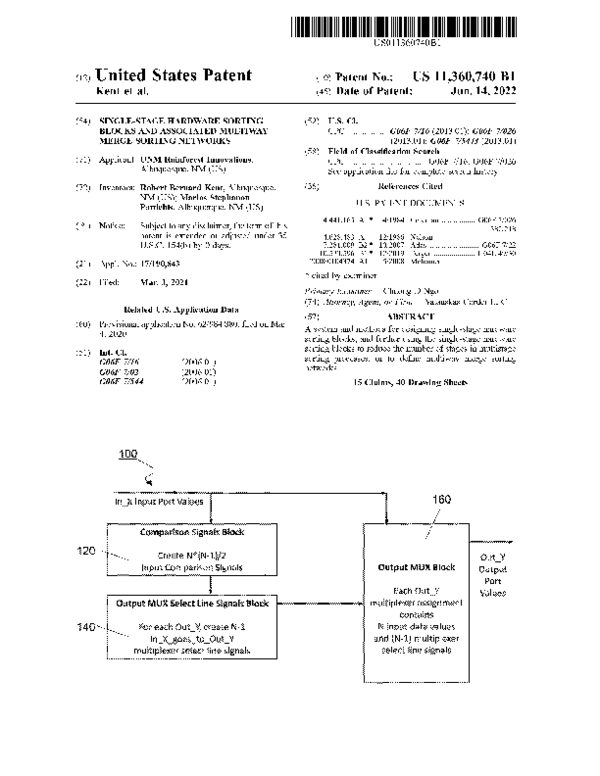
 Marios Pattichis