684
IEEE TRANSACTIONS ON POWER ELECTRONICS, VOL. 17, NO. 5, SEPTEMBER 2002
Unified Steady-State Analysis of Soft-Switching
DC–DC Converters
Jaber Abu-Qahouq, Student Member, IEEE, and Issa Batarseh, Senior Member, IEEE
Abstract—In this paper, based on the switching cell approach,
a unified steady state analysis for families of soft-switching
dc–dc converters with complete unified design equations will be
presented. The concept of the unified approach and step by step
procedure for a generalized process are discussed and applied
to selected soft-switching families such as zero-voltage-switching
(ZVS) and zero-current-switching (ZCS)–quasi-resonant converter families, ZVS-clamped voltage quasi-square-wave (QSW)
family, ZCS-clamped-current (CC) QSW family, and zero-voltagetransition and zero-current-transition pulse-width modulation
families. Also, it has been noted that all the analyzed families
have one generalized transformation table. The basic unified
equations will be summarized and the cell-to-cell comparison will
be introduced. It will be shown that the unified analysis leads to
several advantages such as improving the computer-aided analysis
and design, simplified mathematical modeling, and giving more
insight into the converter-cell operation.
Index Terms—Converter, dc–dc, generalized analysis, softswitching, steady-state, switching-cell, unified analysis, zerocurrent switching, zero-voltage switching.
I. INTRODUCTION
O
VER THE LAST ten years, many soft-switching dc–dc
converter families were introduced in the open literature
with the objectives of developing high switching converters with
high power density and high efficiency [1]–[13]. This was accomplished by adding additional components to the power stage
to either limit the resonant period and/or to utilize power device
parasitic components. As a result of adding an additional auxiliary circuitry (additional resonant components and auxiliary
switches and diodes), the steady-state analysis of soft-switching
topologies tend to be cumbersome, time consuming, and provided little insight into the converter switching cell operation.
In this paper, it will be shown that the analyses of the
soft-switching dc–dc converters can be unified for a given
switching network family. As a result, instead of analyzing individual converter topology, only one switching network for each
family is needed to be analyzed. By using generalized parameters, it is possible to generate a single transformation table from
which the voltage converter ratios and other important design
parameters for each converter can be obtained directly. The
derivation of the model is obtained from studying the switching
network modes of operation and by expressing the switching
intervals in terms of the converter design parameters such as
Manuscript received February 15, 2001; revised February 16, 2002. Recommended by Associate Editor N. Femia.
The authors are with the School of Electrical Engineering and Computer
Science, University of Central Florida, Orlando, FL 32816 USA (e-mail:
batarseh@mail.ucf.edu).
Publisher Item Identifier 10.1109/TPEL.2002.802195.
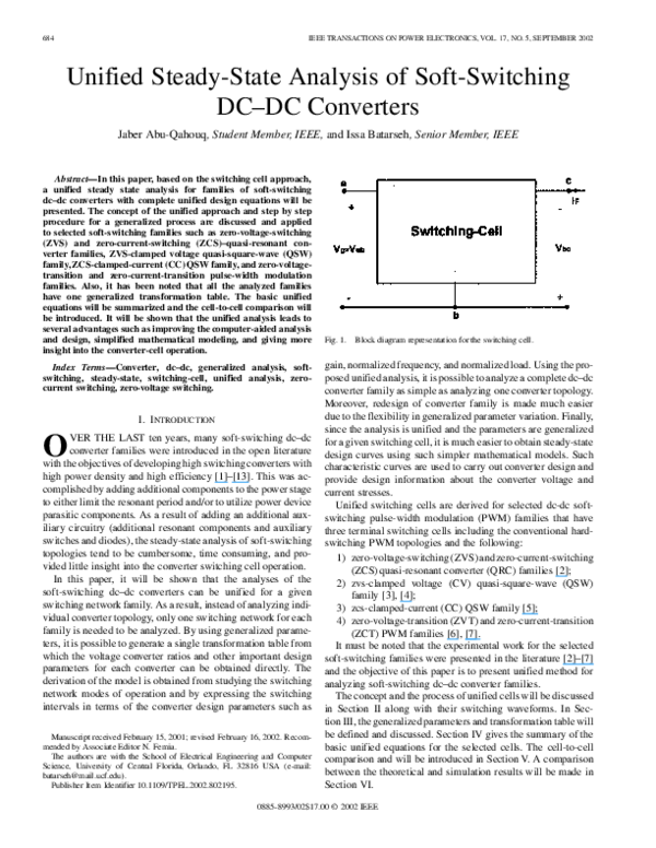
Fig. 1.
Block diagram representation for the switching cell.
gain, normalized frequency, and normalized load. Using the proposed unified analysis, it is possible to analyze a complete dc–dc
converter family as simple as analyzing one converter topology.
Moreover, redesign of converter family is made much easier
due to the flexibility in generalized parameter variation. Finally,
since the analysis is unified and the parameters are generalized
for a given switching cell, it is much easier to obtain steady-state
design curves using such simpler mathematical models. Such
characteristic curves are used to carry out converter design and
provide design information about the converter voltage and
current stresses.
Unified switching cells are derived for selected dc-dc softswitching pulse-width modulation (PWM) families that have
three terminal switching cells including the conventional hardswitching PWM topologies and the following:
1) zero-voltage-switching (ZVS) and zero-current-switching
(ZCS) quasi-resonant converter (QRC) families [2];
2) zvs-clamped voltage (CV) quasi-square-wave (QSW)
family [3], [4];
3) zcs-clamped-current (CC) QSW family [5];
4) zero-voltage-transition (ZVT) and zero-current-transition
(ZCT) PWM families [6], [7].
It must be noted that the experimental work for the selected
soft-switching families were presented in the literature [2]–[7]
and the objective of this paper is to present unified method for
analyzing soft-switching dc–dc converter families.
The concept and the process of unified cells will be discussed
in Section II along with their switching waveforms. In Section III, the generalized parameters and transformation table will
be defined and discussed. Section IV gives the summary of the
basic unified equations for the selected cells. The cell-to-cell
comparison and will be introduced in Section V. A comparison
between the theoretical and simulation results will be made in
Section VI.
0885-8993/02$17.00 © 2002 IEEE
�ABU-QAHOUQ AND BATARSEH: ANALYSIS OF SOFT-SWITCHING DC–DC CONVERTERS
685
Fig. 2. Switching cells: (a) Conventional cell, (b) ZVS-QRC cell, (c) ZCS-QRC cell, (d) ZVS-QSW CV cell, (e) ZCS-QSW CC cell, (f) ZVT-PWM cell, and
ZCT-PWM cell.
II. UNIFIED SWITCHING-CELLS
The block diagram representation for a unified three-terminal
switching cell is given in Fig. 1. Fig. 2 shows the six softswitching cells for the families mentioned above in addition to
the conventional cell, while Fig. 3 shows the basic switching
waveforms for the soft switching cells. Since each family uses
the same switching network (same modes of operation) and the
same waveform shapes, the analysis can be unified using the
following steps.
1) Identify the unified switching cell and the generalized parameters for the given family.
2) Identify the unified switching waveforms for the unified
switching cell.
3) Analyze the switching network modes of operation.
4) Derive the time interval for each mode.
5) Use the switching network output side to derive the gain.
As an example, if the output side is a diode, use the
diode voltage or the diode current, whatever available and
easier, to derive the gain. Or in general, find another equation that relates the cell output to the cell input.
6) Normalize and unify the resultant equations by defining
suitable normalized parameters.
7) Use the unified analysis done in steps 1–6 to derive the
stress equations and other design parameters for the converter detailed analysis and design.
III. GENERALIZED PARAMETERS
TRANSFORMATION TABLE
AND
Various orientations of any of the cells in Fig. 2 result in a
family of converters. Using the three terminals , , and in
the switching cells, generalized parameters can be defined and
their values can be determined from the orientation of the cell
in a specific converter. Let us define the following parameters:
: overall input-to-output converter voltage gain,
1)
;
: normalized cell-input voltage to the converter input
2)
voltage,
;
: normalized cell-output current to the converter
3)
;
output current,
: normalized filter capacitor ( ) voltage to the con4)
;
verter input voltage,
�686
IEEE TRANSACTIONS ON POWER ELECTRONICS, VOL. 17, NO. 5, SEPTEMBER 2002
Fig. 3. Switching cells basic waveforms: (a) ZVS-QRC cell, (b) ZCS-QRC cell, (c) ZVS-QSW CV cell, (d) ZCS-QSW CC cell, (e) ZVT-PWM cell, and
(f) ZCT-PWM cell.
5)
: normalized cell-output voltage to the converter
;
input voltage,
6)
: normalized cell-current entering node
;
verter output current,
to the con-
�ABU-QAHOUQ AND BATARSEH: ANALYSIS OF SOFT-SWITCHING DC–DC CONVERTERS
TABLE I
GENERALIZED TRANSFORMATION TABLE
687
IV. UNIFIED ANALYSIS RESULTS FOR THE SELECTED FAMILIES
Table II shows the basic unified equations (the intervals and
gain equations) for the selected soft-switching cells. Because
of the simplicity of the conventional cell unified analysis, it is
not included in the table. However, it can be shown that the unified basic gain equations for the conventional cell under the continuous conduction mode (CCM) and discontinuous conduction
mode (DCM) operations are
(1)
(2)
7)
8)
: characteristic impedance,
;
: normalized load,
, where
is the converter load resistor;
, where
is the
9) : switching frequency,
switching period;
;
10) : resonant frequency,
;
Where
: normalized frequency,
;
11)
12) : duty ratio of the main switch;
: duty ratio of the auxiliary switch;
13)
,
,
,
14)
,
,
,
: The conduction intervals for the modes
of operation. Note that the end of the switching period
time is also equal to
.
The unified equations for each cell shown in Fig. 2 will include one or more of the following previous defined normalized
,
,
,
,
,
), depending on the
parameters (
topology of the switching cell itself. It must be noted that all the
voltages are normalized with respect to
, while all the current are normalized with respect to .
By applying the switching cells of Fig. 2 to the conventional
dc–dc converters (Buck, Boost, Buck-Boost, Cuk, Zeta, and
SEPIC), a transformation table for each family can be generated. It is interesting to point out that when two or more
switching cells share the same normalized parameter, they will
have the same transformation quantity for that parameter. So,
one transformation table can be generalized for all the families
and only the parameter that is applicable for specific family
unified equations can be used. It can be shown that the single
transformation table given in Table I is complete and applies
to all the cells given in Fig. 2.
The characteristics of this table can be summarized as
follows.
1) As mentioned above, when two or more switching cells
share the same generalized parameter, they will have the
same transformation quantity for that parameter.
2) By applying the theory of conservation of energy, it can
.
be shown that
3) By applying KVL and KCL to the cells, we have:
.
4) As a result of the above-mentioned characteristics, the generalized parameters of the switching cells of Fig. 2 can be
and
.
reduced to only two generalized parameters:
is the ratio of the time when both the switch and
where
the diode are OFF.
It must be noted that the unified analysis of the conventional
cell can be extended by including the inductor at node and analyzing the cell for both modes of operation (CCM and DCM).
The following assumption have been made when the softswitching cells in Fig. 2 are analyzed.
1) The circuit is under steady-state operation.
2) The transistors and diodes are ideal devices.
3) The reactive elements are lossless, linear, passive, timeinvarient, and do not have parasitic components.
passes through is very
4) The filter inductor in which
is constant (constant current source).
large so that
5) The output and filter capacitors are much larger than the
resonant capacitor and can be treated as a constant voltage
sources.
6) All inductors are much larger than the resonant inductor
and can be treated as constant current sources.
7) The switching frequency is less than the resonant frequency.
The unified equations of Table II can be validated to a specific
converter by substituting for the generalized parameters from
Table I. These equations can be used to plot the characteristic
curves for the design purposes.
Many other unified equations can be also derived such as
component stresses. The next section will include some of these
equations.
V. CELL-TO-CELL COMPARISON BASED
UNIFIED EQUATIONS
ON THE
The unified equations can be used to make a cell-to-cell comparison. As an example, Table III shows the unified equations
for the peak and average current and voltage for the main switch,
while Table IV shows the main diode peak voltage and current
for the analyzed ZVS and ZCS cells.
They show how the QRC, QSW, and soft-switching transition
cells voltage and current stresses on the main switch and main
diode are compared. As an example, the following can be concluded from these two tables.
1) The peak voltage stress on the main switch for the
ZVS-QRC cell is high and load ( ) dependent. The higher
the used in the design for the ZVS-QRC cell, the lower
the peak voltage stresses on the main switch. Unlike the
ZVS-QRC cell, the ZVS-CV QSW cell has the peak
. Unfortunately, the peak switch
voltage limited to
�688
IEEE TRANSACTIONS ON POWER ELECTRONICS, VOL. 17, NO. 5, SEPTEMBER 2002
TABLE II
BASIC UNIFIED EQUATIONS SUMMARY
TABLE III
SOME OF THE MAIN SWITCH UNIFIED STRESS EQUATIONS
TABLE IV
SOME OF THE DIODE UNIFIED STRESS EQUATIONS
current for the ZVS-CV QSW cell is higher than twice of
its value in the ZVS-QRC cell and it is load dependent. The
ZVT-PWM cell has low peak voltage and peak current
stresses on the main switch that is also load independent.
2) The peak current stress on the main switch for the
ZCS-QRC cell is high and load dependent. The lower the
, the lower the peak current stress is. For the ZCS-CC
QSW cell, the peak current stress is reduced and it is
load independent, but the peak voltage stress on the main
switch is higher than twice of its value for the ZCS-QRC
cell. In the ZCT-PWM cell, the peak switch current is
high but load independent, while the switch peak voltage
stress is kept low.
�ABU-QAHOUQ AND BATARSEH: ANALYSIS OF SOFT-SWITCHING DC–DC CONVERTERS
689
TABLE V
SOME CHARACTERISTICS FOR THE ANALYZED CELLS
3) The average main switch voltage is the same for all the
.
analyzed switching cells and is equal to
4) The ZVS-CV QSW cell causes the current stress on the
diode to increase and to be load dependent by trying to reduce the voltage stress on the main switch. In the ZCS-CC
QSW cell, the voltage stress on the diode increases and
is load dependent, while the current stress on the main
switch is lower.
5) The ZVT-PWM and the ZCT-PWM cells reduce the current and the voltage stresses on the main switch without
increasing it on the diode.
Table V summarized some characteristics for the analyzed
soft-switching cells.
Furthermore, the unified analysis can be used to derive other
characteristic equations for the unified switching cells such as
values as shown below for the
the component stresses and
ZCT-PWM cell [14], [15].
resonant inductor current
1) Unified equation for
) as seen in the equation shown at the bottom
(
of the page. After normalizing by dividing the above
equation by , the expression for the normalized
resonant inductor current will be the equation shown at
the bottom of the next page, which yields
(3)
2) Unified equation for peak resonant capacitor voltage
).
(
It can be shown that
(4)
3) Unified equation for peak resonant inductor current
).
(
It can be shown that
(5)
VI. DESIGN EXAMPLE AND SIMULATION RESULTS
After comparing between the cells, an appropriate cell for
specific design requirements can be chosen. As an example,
�690
IEEE TRANSACTIONS ON POWER ELECTRONICS, VOL. 17, NO. 5, SEPTEMBER 2002
=
Fig. 4. Some characteristics curves for the ZCT-PWM boost: (a) dc voltage conversion ratio characteristics for f
0.5, (b) normalized resonant inductor rms
0.5, (c) normalized resonant inductor peak current, and (d) normalized resonant capacitor peak voltage for
0.427.
current for f
=
the ZCT-PWM cell is chosen here. Once a cell is selected, design curves may be plotted using the unified equations along
with Table I. Fig. 4 shows some of these design curves for the
ZCT-PWM boost converter.
V and
A 10 W ZCT-Boost DC-DC converter with
V is to be designed here for
and
.
A step by step design procedure is given as follows.
1)
2) From the gain equation in Fig. 4(a), we have
.
3) The load resistance is
, and the
A.
load current is
KHz, and with
, the
4) By choosing
resonant frequency is
KHz.
, the characteristics impedance
5) By choosing
.
becomes
=
6) Solve the following two equations
and
:
kHz
to yield
H and
7) The time interval when
culated from
, which means that
nF
should be ON (
) can be cal-
�ABU-QAHOUQ AND BATARSEH: ANALYSIS OF SOFT-SWITCHING DC–DC CONVERTERS
Fig. 5.
ZCT-PWM boost basic waveforms from Pspice simulation results.
TABLE VI
THEORETICAL AND SIMULATION RESULTS COMPARISON
Fig. 5 shows the basic waveforms from the simulation results
using Pspice while Table VI shows a comparison between some
values from the theoretical results and the Pspice simulation results. This table shows that the theoretical and the simulation
results are in good agreement.
691
[2] K. Liu, R. Oruganti, and F. C. Lee, “Resonant switches—Topologies and
characteristics,” IEEE Trans. Power Electron., vol. PE-2, pp. 62–74, Jan.
1987.
[3] V. Vorpe’rian, “Quasisquare-wave converters: Topologies and analysis,”
IEEE Trans. Power Electron., vol. 3, pp. 183–191, Mar. 1998.
[4] T. Mizoguchi, T. Ohgai, and T. Ninomiya, “A family of single-switch
ZVS-CV DC-DC converters,” in Proc. IEEE APEC’94, vol. 2, 1994,
pp. 1392–1398.
[5] E. Ismail and A. Sebzali, “A new class of quazi-square wave resonant
converters with ZCS,” in Proc. IEEE APEC’97, 1997, pp. 1381–1387.
[6] G. Hua, C. Leu, and F. C. Lee, “Novel zero-voltage-transition PWM
converters,” in Proc. IEEE PESC’92, 1992, pp. 55–61.
[7] G. Hua, E. X. Yang, Y. Jiang, and F. C. Lee, “Novel zero-current-transition PWM converters,” IEEE Trans. Power Electron., vol. 9, pp.
601–606, Nov. 1994.
[8] G. Hua and F. Lee, “Evaluation of switched-mode power conversion
topologies,” in Proc. 1st Int. Power Electronics Motion Control Conf.
(IPEMC), vol. 1, 1994, pp. 12–26.
[9] A. B. Carlson, Circuits. Pacific Grove, CA: Brooks/Cole-Thomson
Learning, 2000.
[10] C. Tseng and C. Chen, “Zero-voltage-transition topologies for Cuk converters,” in Proc. IEEE PESC’98, vol. 2, 1998, pp. 930–935.
, “On the ZVT-PWM Cuk converter,” IEEE Trans. Ind. Electron.,
[11]
vol. 45, pp. 674–677, Aug. 1998.
[12] D. C. Martins and G. N. de Abreu, “Application of the ZETA converter
in switch-mode power supplies,” in Proc. IEEE APEC’93, 1993, pp.
214–220.
[13] C. H. G. Treviso, O. C. De Freitas, and V. J. Farias, “A ZVS-ZCS-PWM
self-resonant dc-dc sepic converter,” Ind. Electron., Control Instrum.,
vol. 1, pp. 176–181, 1994.
[14] J. Abu-Qahouq, “Generalized analysis of soft-switching dc–dc converter
families,” Tech. Rep., Univ. Central Florida, Orlando, 2000.
[15] J. Abu-Qahouq and I. Batarseh, “Generalized analysis of soft-switching
DC-DC converters,” in Proc. IEEE PESC’00, vol. 1, 2000, pp. 185–192.
Jaber Abu-Qahouq (S’01) received the B.Sc.
degree in electronics engineering from Princess
Sumaya University, Amman, Jordan, in 1998,
and the M.S. degree in electrical engineering and
electronics from the University of Central Florida,
Orlando, in 2000, where he is currently pursuing the
Ph.D. degree.
He worked as a Test Engineer in the Electronic
Services and Training Center, Royal Scientific Society, Amman, Jordan. His research interests include
soft-switching power conversion, power factor correction circuits, and low-voltage high-current fast-transient dc–dc converters.
His research results in publishing several research papers.
Mr. Abu-Qahouq received several awards, including the Royal Watch.
VII. CONCLUSION
A unified analysis method for families of soft-switching
dc–dc converters was developed in this paper. The unified
technique is applied to several well-known switching families
including QRC, QSW, and PWM converters. It is shown that
there exists a single Generalized Transformation Table for all the
families. This leads to several advantages such as improving the
computer-aided analysis and design, simplified mathematical
modeling, and gives more insight into the converter-cell operation. The unified equations for each family can be easily used in
the analysis of any new converter that uses the same switching
cell. This is done by finding the generalized parameters for the
new converter and then substituting in the unified equations.
The cell-to-cell comparison was introduced and the theoretical
results were compared with the simulation results.
REFERENCES
[1] E. J. Miller, “Resonant switching power conversion,” in Proc. IEEE
PESC’76, 1976, pp. 206–211.
Issa Batarseh (SM’93) received the B.S., M.S.,
and Ph.D. degrees from the University of Illinois,
Chicago, in 1983, 1985, and 1990, respectively, all
in electrical engineering.
He is a Professor in the School of Electrical Engineering and Computer Science, University of Central
Florida (UCF), Orlando. He was a Visiting Assistant
Professor at Purdue University, West Lafayette, IN,
from 1989 to 1990, before joining UCF in 1991. His
power electronics research focuses on the development of high frequency power converters to improve
power density, power factor, efficiency, and performance. The research includes
the analysis and design of high frequency dc-to-dc resonant converter topologies, low-voltage dc-dc converters, small signal modeling and control of PWM
and resonant converters, power factor correction techniques, and power electronic circuits for distributed power systems applications.
Dr. Batarseh has served as a Chairman of the PE/AES/PEL Chapter, Orlando IEEE Section and currently serves as an ExCom member of the lEEE
Orlando Section. He is also an Associate Editor for the IEEE TRANSACTIONS
ON AEROSPACE AND ELECTRONIC SYSTEMS and the IEEE TRANSACTIONS ON
CIRCUITS AND SYSTEMS. He is a Reviewer for the National Science Foundation
and several IEEE TRANSACTIONS/JOURNALS. He serves on the program committees of IEEE-APEC, PESC, IECON, IAS, and ISCAS. He is a Registered
Professional Engineer in Florida.
�
 Massimo Vitelli