Real-time Control Systems - é»åé»å 系統èæ¶çè¨è¨å¯¦é©å®¤ - åç« ...
Real-time Control Systems - é»åé»å 系統èæ¶çè¨è¨å¯¦é©å®¤ - åç« ...
Real-time Control Systems - é»åé»å 系統èæ¶çè¨è¨å¯¦é©å®¤ - åç« ...

You also want an ePaper? Increase the reach of your titles
YUMPU automatically turns print PDFs into web optimized ePapers that Google loves.
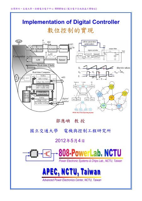
台 灣 新 竹 ‧ 交 通 大 學 ‧ 前 瞻 電 力 電 子 中 心 808 實 驗 室 ( 電 力 電 子 系 統 與 晶 片 實 驗 室 )<br />
Implementation of Digital <strong>Control</strong>ler<br />
數 位 控 制 的 實 現<br />
鄒 應 嶼<br />
教 授<br />
國 立 交 通 大 學<br />
電 機 與 控 制 工 程 研 究 所<br />
2012 年 5 月 4 日<br />
Power Electronic <strong>Systems</strong> & Chips Lab., NCTU, Taiwan<br />
Advanced Power Electronics Center, NCTU, Taiwan
<strong>Real</strong>-<strong>time</strong> <strong>Control</strong> <strong>Systems</strong>: A Tutorial<br />
A. Gambier<br />
Automation Laboratory, B6 23-29, EG. Bauteil C<br />
University of Mannheim, 68131 Mannheim, Germany<br />
gambier@ti.uni-mannheim.de<br />
Abstract<br />
The literature about real-<strong>time</strong> systems presents digital<br />
control or computer controlled systems as one of its most<br />
important practical application field. However, it is very<br />
difficult to find in these textbooks real-<strong>time</strong> control aspects.<br />
It seems to be more natural that these applications should<br />
be treated as part of digital control courses. In spite of<br />
that, control system literature rarely includes extensively<br />
the real-<strong>time</strong> subject and it does normally not pay attention<br />
to real-<strong>time</strong> aspects beyond algorithms and choice of sampling<br />
<strong>time</strong>s. The aim of this paper is to highlight important<br />
issues about real-<strong>time</strong> systems that should be taken into<br />
account at the moment to implement digital control.<br />
1 Introduction<br />
The implementation of digital control systems and real-<strong>time</strong><br />
systems belong together and they should be connected<br />
more or less later in the control engineering curricula.<br />
However, it is difficult to find this connection in the<br />
standard textbooks, where the real-<strong>time</strong> implementation is<br />
almost always ignored. For example, a very good introduction<br />
into computer controlled systems can be found in [1],<br />
but no orientation to the real-<strong>time</strong> software is given there.<br />
Mechanisation of control algorithms are given e.g. in [9].<br />
In [8], hardware and software for digital control systems<br />
are described shortly. On the other hand, in [3] the real<strong>time</strong><br />
system design is treated from the optic of control<br />
engineering without to consider implementation aspects.<br />
In general, real-<strong>time</strong> issues are gradually becoming “transparent”<br />
to the control engineering student. This transparency<br />
has been considerably increased in the last years with the<br />
advent of software tools like Matlab/Simulink ([24]) with<br />
its RTW (<strong>Real</strong> Time Workshop), the RTWT (<strong>Real</strong> Time<br />
Windows Target) and products from other companies like<br />
WinCon from Quanser ([25]) and ECP Executive from ECP<br />
<strong>Systems</strong> ([26]). They certainly do the implementation of<br />
real-<strong>time</strong> experiments easier and save much <strong>time</strong>, but on<br />
the other hand they put more distance regarding to the reallife<br />
problems, which can emerge during the real-<strong>time</strong> implementation<br />
of control systems. Hence, control concepts<br />
become today easier to be exemplified, but control engineering<br />
students can lose the real dimension about designing<br />
real-<strong>time</strong> control systems, particularly when they have to<br />
deal with <strong>time</strong>-critical applications.<br />
This paper attempts to give an introduction to the implementation<br />
of real-<strong>time</strong> control systems, where characteristics<br />
of real-<strong>time</strong> systems and digital control issues are taking together<br />
into account.<br />
The outline of the paper is as follow. Digital control aspects<br />
are introduced in Section 2. Definitions and characteristics<br />
of real-<strong>time</strong> systems are described in Section 3. Here, some<br />
common mistakes and misconceptions by developing real<strong>time</strong><br />
control software are also discussed. Section 4 treats the<br />
implementation of real-<strong>time</strong> controllers and Section 5 summarizes<br />
some important specifications for the implementation<br />
of real-<strong>time</strong> control systems as well as some well-known<br />
commercial products. Finally, conclusions are drawn in<br />
Section 6.<br />
2 Computer controlled systems<br />
The introduction of digital computers in the control loop<br />
has allowed developing more flexible control systems<br />
including higher-level functions and advanced algorithms.<br />
Furthermore, most current complex control systems could<br />
not be implemented without the application of digital hardware.<br />
However, the simple sequence sensing–control–actuation<br />
for the classical feedback control becomes more complex<br />
as well. Nowadays, this sequence can be supplemented<br />
as follow: sensing–data acquisition–control law<br />
calculation–actuation–data base update. Figure 1 shows<br />
an overview of such control systems.<br />
User<br />
Computer<br />
User<br />
Supervisory<br />
control<br />
u(k)<br />
D/A Hold<br />
y m (k)<br />
GUI<br />
<strong>Real</strong>-<strong>time</strong> Computer<br />
u(k)<br />
r(k)<br />
A/D<br />
Scaling<br />
unitsvoltage<br />
voltagedig. number<br />
<strong>Control</strong> Algorithm<br />
u(k) = f [y(k), r(k)]<br />
From other<br />
control level<br />
Scaling<br />
voltage units<br />
dig. numbervoltage<br />
u(t)<br />
Actuator<br />
y m (t)<br />
<strong>Real</strong>-<strong>time</strong> Clock<br />
Port<br />
y(k)<br />
Port<br />
Process<br />
Sensor<br />
u(k)<br />
digital<br />
number<br />
Figure 1. Overview of a computer controlled system<br />
y(t)
Thus, the control system now contains not only wired components<br />
but also algorithms, which must be programmed,<br />
i.e. software is now included in the control loop. This<br />
leads to new aspects to take into account by designing<br />
control systems:<br />
1.Errors due to A/D and D/A conversion as well as due<br />
to limited length word calculations. This subject is<br />
well treated in the literature (see for example [ 9]).<br />
2. Software developing is prone to errors. Thus, a new<br />
concept has to be introduced to consider this aspect, the<br />
verification, i.e. a mechanism to test if the software is<br />
doing exactly what it is expected. Here it is necessary<br />
to remark that in general a high percent of errors in<br />
digital control systems are caused by programming<br />
mistakes. Hence, digital control projects need not<br />
only control engineers but also engineers with skills in<br />
software engineering and computer programming.<br />
3. Standard textbooks on digital control systems normally<br />
assume that sampling is uniform, periodic and synchronous.<br />
This leads to a case of “zero-<strong>time</strong>-execution” for<br />
the control law. However, that is not realistic since the<br />
control algorithm also consumes some <strong>time</strong> producing a<br />
control or feedback delay (control or feedback latency),<br />
i.e. a delay between a sampling instant and the instant<br />
at which a control-signal value is applied to the actuator.<br />
If the controller design is based on a model and the<br />
delay is constant and known, it could be helpful to use a<br />
tool for the description of the inter-sample behaviour<br />
(e.g. modified z-transform) in order to obtain a discrete<strong>time</strong><br />
model more approximated to the real case.<br />
4.The computational <strong>time</strong> of control algorithms can<br />
change from one sampling instant to other (e.g. hybrid<br />
controller with controller switching mechanism, event<br />
based controllers, adaptive controllers with on-line<br />
parameter update, etc.). This variation in the delay is<br />
called control jitter (according to the IEEE, jitter is “the<br />
<strong>time</strong>-related abrupt, spurious variation in the duration<br />
of any specified related interval”). Moreover, value<br />
calculation for the control signal is usually carried out<br />
using multitasking (Subsection 3.2) defining a set of<br />
control tasks with respective priorities. Thus, a task can<br />
be pre-empted by higher priority tasks. In general, it<br />
can be said that the control system is also affected by<br />
several kind of jitter depending on context: sampling<br />
jitter, control latency jitter, input jitter, output jitter, etc.<br />
Finally, real-<strong>time</strong> issues are often ignored in the implementation<br />
of digital control systems. This is in part a consequence<br />
of erroneous definitions and false interpretations.<br />
Popular misconceptions from the control engineering<br />
community about real-<strong>time</strong> systems are for example:<br />
The computer was connected to the plant by mean of<br />
A/D and D/A converters in order to obtain the real<strong>time</strong><br />
system. Analog plants should be connected to the<br />
computer through A/D and D/A converters. This link<br />
with the “real world” does not lead to a real-<strong>time</strong><br />
system. On the other hand, it is possible to find real<strong>time</strong><br />
systems in complete digital contexts.<br />
Our plant is so slow that real <strong>time</strong> is actually no<br />
problem. A slow control system, which does not need<br />
a fast computer, can require critical <strong>time</strong> constraints.<br />
It is also possible that a control system does no need<br />
any hard real-<strong>time</strong> requirements but it is not necessarily<br />
a consequence of the slow plant.<br />
It is not meaningful to talk about guarantying real-<strong>time</strong><br />
performance. It is true that occasionally <strong>time</strong> constraints<br />
can be relaxed without introducing additional problems<br />
in the control loop. This particularly applies to nice designed<br />
laboratory experiments. However, this actually<br />
depends on the application, and the <strong>time</strong> criticality<br />
should be proved for each individual case. On the other<br />
hand, real-<strong>time</strong> performance cannot be 100% guaranteed<br />
while hardware and software failures cannot be avoided<br />
at all.<br />
We do not care about real <strong>time</strong> in our digital control<br />
system and even though it works. This statement is<br />
similar to the previous one. The problem here is that<br />
you are not able to know when your system can fail.<br />
<strong>Real</strong>-<strong>time</strong> programming is assembly coding, priority<br />
interrupt programming and device driver writing. It<br />
is true that some code is still writing in assembler.<br />
However, high programming languages like C, Ada<br />
95, Modula 2 and <strong>Real</strong>-<strong>time</strong> Java are normally used<br />
to develop real-<strong>time</strong> software. Device driver programming<br />
is necessary for real-<strong>time</strong> as well as non-real<strong>time</strong><br />
systems but they should be provided by the operating<br />
system or by the device manufacturer. Interrupt<br />
programming should be in principle avoided as much<br />
as possible. This point is treated in Subsection 3.5.<br />
In the next Sections, an overview about real-<strong>time</strong> systems<br />
and control systems will be given in order to clarify real-<strong>time</strong><br />
programming and its most important application.<br />
3 <strong>Real</strong>-<strong>time</strong> systems: a short introduction<br />
<strong>Real</strong>-<strong>time</strong> computing is a vast field and therefore, a complete<br />
discussion about that is outside the scope of this paper.<br />
Therefore, only the most relevant aspects will be treated here.<br />
3.1 Definitions and general aspects<br />
It is possible to find in the literature several definitions for<br />
real-<strong>time</strong> systems. Here, a definition that does not contradict<br />
the definition given in the IEEE POSIX Standard (Portable<br />
Operation System Interface for Computer Environments)<br />
will be assumed<br />
A real-<strong>time</strong> system is one in which the correctness of a<br />
result not only depends on the logical correctness of<br />
the calculation but also upon the <strong>time</strong> at which the<br />
result is made available.<br />
This definition emphasizes the notion that <strong>time</strong> is one of<br />
the most important entities of the system, and there are<br />
timing constraints associated with systems tasks. Such<br />
tasks have normally to control or react to events that take<br />
places in the outside world, which are happening in “real<br />
<strong>time</strong>”. Thus, a real-<strong>time</strong> task must be able to keep up with<br />
external events, with which it is concerned.
It should be noted here that real-<strong>time</strong> computing is not<br />
equivalent to fast computing. Fast computing aims at getting<br />
the results as quickly as possible, while real-<strong>time</strong> computing<br />
aims at getting the results at a prescribed point of <strong>time</strong> within<br />
defined <strong>time</strong> tolerances. Thus, a deadline (for this point of<br />
<strong>time</strong>) can be associated with the task that has to satisfy this<br />
timing constraint specifying either its start or completion <strong>time</strong>.<br />
If the task has to meet the deadline, because otherwise it<br />
will cause fatal errors or undesirable consequences, the<br />
task is called hard real-<strong>time</strong> task. On the contrary, if the<br />
meeting of the deadline is desirable but not mandatory, the<br />
task is said to be a soft real-<strong>time</strong> task. By extension, one<br />
speaks about hard/soft <strong>time</strong>-constraints as well as hard/soft<br />
deadlines.<br />
3.2 <strong>Real</strong>-<strong>time</strong> operating systems (RTOS)<br />
In order to implement multitasking real-<strong>time</strong> systems, two<br />
approaches can be used: The first one consists in programming<br />
by using concurrent real-<strong>time</strong> languages and the<br />
second one is to use a sequential language and a real-<strong>time</strong><br />
operating system ([4]). There has been a long debate about<br />
advantages and drawback of both approaches, which will not<br />
be treated here. However, a very important point is that<br />
real-<strong>time</strong> systems and real-<strong>time</strong> operating systems are not<br />
equivalent concepts: A RTOS provides facilities, like<br />
multitasking (i.e. concurrency or potential parallelism),<br />
scheduling, intertask communication mechanism, etc., for<br />
implementing real-<strong>time</strong> systems.<br />
Old operating systems are characterised by the fact that each<br />
task is a simple program running in its own memory space.<br />
In the last years, there has been a tendency to provide facilities<br />
for creating several tasks within the same program to<br />
have faster task switch, unrestricted access to shared memory<br />
and to simplify the communication and synchronization.<br />
Such tasks are commonly called threads. The most<br />
important disadvantage of using threads consists in that the<br />
memory is not protected between threads of the same<br />
program. Figure 2 illustrates the difference between<br />
multitasking and multithread systems.<br />
M ultitasking<br />
M ultitasking<br />
One Thread<br />
M ultithread<br />
Task 1 Task n Task 1<br />
Task n<br />
Program 1 Program n Program 1 Program n<br />
Figure 2. Multitasking and multithreading concepts<br />
Together with parallelism, determinism is another important<br />
property of RTOS. A RTOS is predictable if the <strong>time</strong><br />
necessary to acknowledge a request of an external event is<br />
know in advance. The end point of this predictability<br />
scale is called determinism, in sense that this <strong>time</strong> is<br />
exactly known in advance. This concept should not be<br />
confused with responsiveness, which is the <strong>time</strong> (after the<br />
acknowledgement) elapsed till the request is attended.<br />
Determinism and responsiveness make up the response <strong>time</strong><br />
to external events. This is also called system latency.<br />
Modern RTOS include in general the following features:<br />
fast switch context, small size, preemptive scheduling based<br />
on priorities, multitasking and multithreading, intertask communication<br />
and synchronisation mechanisms (semaphores,<br />
signals, events, shared memory, etc.), real-<strong>time</strong> <strong>time</strong>rs, etc.<br />
However, RTOS are similar to standard operating systems<br />
from a structural point of view, since functional components<br />
as interrupt handler, task manager, memory manager, I/O<br />
subsystem and intertask communication are proper of both<br />
kind of operating systems.<br />
3.3 <strong>Real</strong>-<strong>time</strong> scheduling<br />
The distinctive part of a RTOS is the task manager. It is<br />
composed by the Dispatcher and the Scheduler. The Dispatcher<br />
carries out the context switch, i.e. the parameter<br />
saving for the outgoing task and the parameter loading for<br />
the incoming task, and the CPU handing over to the task<br />
that is becoming active.<br />
The Scheduler has the function of selecting the task, which<br />
will obtain the processor as next. This choice is given by<br />
means of algorithms and this is the point where RTOS and<br />
non-RTOS are mostly distinguished. <strong>Real</strong>-<strong>time</strong> systems need<br />
special algorithms to schedule a set of tasks. This is a very<br />
active area of research in computer science and many<br />
algorithms have been proposed. In this paper, only the<br />
most important uniprocessor scheduling algorithms for real<strong>time</strong><br />
requirements will be presented. Fig. 3 presents an<br />
overview about some well-known scheduling algorithms<br />
(for details see e.g. [17], [12]).<br />
Scheduling algorithms can be grouped in two classes: static<br />
and dynamic algorithms. A static scheduling requires that<br />
the complete information about the scheduling problem<br />
(number of tasks, deadlines, priorities, periods, etc.) is<br />
known a priori. Thus, the scheduling problem is solved<br />
before the schedule is executed. Such scheduler is also<br />
called clairvoyant. If at run <strong>time</strong> the feasibility can be<br />
determined and changes in the configuration may be carried<br />
out, then the scheduling is said to be dynamic.<br />
Static schedules must always be planed off-line. Dynamic<br />
schedules can be planed either off-line if the complete<br />
scheduling problem is known a priori but with an on-line<br />
implementation, i.e. the configuration is changed at run<br />
<strong>time</strong>, or on-line if the future is unknown or ignored. Advantage<br />
of off-line scheduling is its determinism and the disadvantage<br />
its inflexibility. On the contrary, an on-line<br />
scheduling is very flexible but poor in determinism. Moreover,<br />
an on-line scheduling does not perform well if the<br />
system is overloaded. However, on-line scheduling is clearly<br />
the only option in a system whole future workload is<br />
unpredictable.<br />
The guarantee that all deadlines are met can be taken as<br />
measure of the effectiveness of a real-<strong>time</strong> scheduling algorithm.<br />
If any deadline is not met, the system is said to be<br />
overloaded. Liu and Layland ([13]) showed that the total<br />
processor utilization for a set of n tasks given by<br />
n C<br />
U i<br />
(1)<br />
min( D , )<br />
i 1 i T<br />
i<br />
can be used as schedulability test. C is the execution <strong>time</strong>,<br />
D the deadline and T the task period. If the task is<br />
aperiodic or the deadline is smaller than the period, then<br />
the deadline is used in the equation. Figure 3 presents a<br />
classification for the most well-known dynamic scheduling<br />
algorithms for uniprocessor systems. In the following, the
most popular algorithms for scheduling tasks with real-<strong>time</strong><br />
requirements will be shortly presented.<br />
Static Scheduling<br />
Scheduling Policies<br />
With Priorities<br />
Dynamic Priorities<br />
Dynamic Scheduling<br />
Without Priorities<br />
Preemptive Non-preemptive Preemptive<br />
Static Priorities<br />
Nonpreemptive<br />
Preemptive<br />
Nonpreemptive<br />
SJF FPS mit Deadline mit Deadline SRT HRRN RR FCFS<br />
<strong>Real</strong>-Time Scheduling<br />
FPS: Fixed-Priority<br />
RMS DMS EDF LLF MUF<br />
FCFS: First Come First served RMS: Rate Monotonic<br />
RR: Round Robin<br />
DMS: Deadline Monot. Scheduling<br />
<strong>Real</strong>-Time Scheduling<br />
FC-EDF<br />
EDF: Earliest Deadline<br />
SJF: Shortest Job First<br />
LLF: Least Laxity First<br />
SRT: Shortest Remaining Time MUF: Maximum Urgency<br />
HRRN: Highest Response Ratio Next FC-EDF: Feedback EDF<br />
Figure 3. Classification of uniprocessor scheduling<br />
algorithms<br />
Fixed-Priority Scheduling (FPS). In this approach, each<br />
task has a fixed static priority which is computed pre-run<br />
<strong>time</strong>. The runnable tasks are executed in the order determined<br />
by their priorities. If all tasks are periodic, a simple<br />
priority assignment can be done according to the statement:<br />
the shorter the period, the higher the priority. This approach<br />
is known as Rate Monotonic Scheduling (RMS) and it was<br />
proposed in [13]. The schedulability analysis for this algorithm<br />
presumes that all tasks are pre-emptive, periodic with<br />
deadlines equal to the period and independent (i.e. no task<br />
precedence between tasks exists). In this case the total<br />
utilization has an upper bound given by<br />
1/ n<br />
U n(2 1)<br />
This bound converges to 0.693 for n , to 0.88 when<br />
the periods are uniform and to 1,00 only when the periods<br />
are harmonics of the smallest period. Under the conditions<br />
given above, it can be showed that the algorithm is<br />
optimal among fixed priority policies (i.e. given a set of<br />
tasks, RMS always produces a feasible schedule for this set,<br />
if any other algorithm can do that). This approach is easy to<br />
be implemented and if there are schedulability problems,<br />
the first task to fail is the task with the longest period, i.e.<br />
if the system becomes overloaded, deadlines are missed predictably.<br />
The most important drawbacks are its low utilization<br />
(under 70%), the fixed priorities, which can lead to<br />
starvation and deadlocks, and the fact that all deadlines<br />
should be equal to the periods.<br />
In order to get out of the last problem, the Deadline Monotonic<br />
Scheduling (DMS) was proposed in [11]. They generalized<br />
the RMS allowing deadlines less than periods,<br />
where the fixed priority of a task is inversely proportional<br />
to its deadline.<br />
(2)<br />
Deadline-based Dynamic Scheduling. There are some dynamic<br />
scheduling algorithms which are based on assigning<br />
priorities according to their deadline. The simplest algorithm<br />
in this class is the Earliest Deadline First algorithm (EDF),<br />
where the task with the earliest (shortest) deadline has the<br />
highest priority. Thus, the resulting priorities are naturally<br />
dynamic. This algorithm can be used for both dynamic and<br />
static scheduling. However, absolute deadline are normally<br />
computed at run <strong>time</strong> and hence the algorithm is presented<br />
as dynamic. This algorithm was also proposed in [ 13] .<br />
They also showed that if all task are periodic and preemptive,<br />
then the algorithm is optimal and its utilization is U 1.<br />
A disadvantage of this algorithm is that the execution <strong>time</strong> is<br />
not taken into account in the priority assignment.<br />
Another algorithm that is also optimal for scheduling preemtive<br />
tasks on one-processor system is the Maximum Laxity<br />
First (MLF) algorithm ([6], also called Least Slack-<strong>time</strong><br />
First, (LSF) or Least Laxity First (LLF) algorithm). At any<br />
<strong>time</strong>, the laxity (or slack) of a task with deadline is equal to<br />
Laxity deadline remaining execution <strong>time</strong> . (3)<br />
The MLF algorithm assigns priorities based on their laxities:<br />
the smaller the laxity, the higher the priority. This algorithm<br />
requires the knowledge of the current execution <strong>time</strong>, and<br />
then laxity is essentially a measure of the flexibility available<br />
for scheduling a task. Thus, MLF takes into consideration the<br />
execution <strong>time</strong> of a task, and this is it advantage in front of<br />
EDF. On the other hand, the execution <strong>time</strong> is normally not<br />
known until the task complete and therefore estimation is<br />
necessary. Because this estimation is used to schedule the<br />
set of task, the resulting schedule can be incorrect. This is<br />
its most serious disadvantage.<br />
The MLF algorithm also has a schedulable bound of 100%<br />
for all task sets. A problem with EDF as well as MLF is<br />
that there is no way to predict which tasks will fail in<br />
transient overboard situations. This has led to another algorithm<br />
called Maximum Urgency First (MUF) algorithm<br />
([19]), where an explicit description of urgency is assigned<br />
to each task. This urgency is defined as a combination of<br />
two fixed priorities, and a dynamic priority, which is<br />
inversely proportional to the task laxity. One of the fixed<br />
priorities, called task criticality has precedence over the<br />
dynamic priority. The other fixed priority, called user<br />
priority, has lower precedence than the dynamic priority.<br />
The criticality helps on-line algorithms to distinguish more<br />
important from less important tasks. Finally, it is necessary<br />
to remark that all mentioned dynamic algorithms do not<br />
remain optimal if pre-emption is not allowed or the system<br />
has multiple processors.<br />
If sporadic or aperiodic tasks must be scheduled, two algorithms<br />
can be used: the Deferrable Server Algorithm (DSA)<br />
and the Sporadic Server Algorithm (SSA). However, only<br />
SSA conforms to the RMS schedulability analysis.<br />
3.4 Intertask Communication and Synchronisation<br />
The intertask communication can be carried out as for<br />
non-RTOS by using mailbox, pipes and shared memory.<br />
Synchronization is very important in real-<strong>time</strong> systems for<br />
two reasons: (i) tasks may experience unpredictable delays<br />
due to blocking on shared resources to which they require<br />
exclusive access (e.g. A/D and D/A converters), and (ii) some<br />
tasks should be executed depending on results of other tasks.<br />
It can be shown that the addition of mutexes in real-<strong>time</strong> programs<br />
makes the general scheduling problem a non-predictable<br />
one ([14]). To solve this problem with an EDF algorithm<br />
kernelized monitor protocol can be used and priority<br />
ceiling protocol if the scheduling algorithm is RMS.<br />
3.5 Common programming mistakes<br />
By programming real-<strong>time</strong> system, many typical mistakes<br />
are often founded ([ 18] ). Some of them are:
Large or many if-then-else and/or case statements.<br />
These statements introduce in the code many different<br />
paths with varying length so that the code will also have<br />
different execution <strong>time</strong>. This becomes more significantly<br />
when the path is very long. Variable functions,<br />
state machines, lookup tables should be used instead the<br />
mentioned statements.<br />
Delays implemented as empty/dummy loops. This leads<br />
to inaccurately delays depending on the hardware.<br />
RTOS timing mechanisms should be used here for<br />
implementing exactly <strong>time</strong> delays.<br />
Indiscriminate use of Interrupts. Interrupts affect seriously<br />
the real-<strong>time</strong> predictability: They cannot be<br />
scheduled, and they have always very high priorities.<br />
Programs based on interrupt are very difficult to debug<br />
and to analyse. Moreover, they operate in kernel<br />
context.<br />
There is a very popular myth, which says that interrupts<br />
save CPU <strong>time</strong> and they guarantee the execution start of<br />
a task. This can be true in small and simple microprocessor<br />
based systems. However, it is not the case for<br />
complex real-<strong>time</strong> system, where non-preemptive periodic<br />
tasks can provide similar latency with better predictability<br />
and CPU utilization.<br />
Periodic polling threads should be used if it is possible.<br />
Interrupt services routines should be programmed in<br />
such a form that its only function is to signal an<br />
aperiodic server.<br />
Configuration information fixed using #define or similar<br />
statements. Programmers frequently use #define statements<br />
in their code to specify register addresses, limits<br />
for arrays, and configuration constants. Although this<br />
practice is common, it is undesirable because it prevents<br />
on-the-fly software patches for emergency situations,<br />
and it increases the difficulty of reusing the software in<br />
other applications. Changes in the configuration require<br />
that the entire application has to be recompiled.<br />
Implementation based on a big single loop. One big<br />
loop leads to the fact that the complete software executes<br />
to the same rate. In order to assign different and<br />
proper rates concurrent techniques for pre-emptive<br />
RTOS should be used.<br />
Use of message passing as primary intertask communication<br />
mechanism. Message passing reduces real-<strong>time</strong><br />
schedulability bound and it produces significant overhead<br />
leading to many aperiodic servers instead of periodic<br />
tasks. Moreover, deadlocks can appear in closed<br />
loops systems. Shared memory and proper synchronization<br />
mechanisms to prevent deadlocks and priority<br />
inversion should be used.<br />
To think that problems can be fixed magically. Programming<br />
errors, which become seldom visible in the<br />
debugging phase, can appear exactly at the <strong>time</strong> when<br />
the application is running and it is not possible to<br />
correct the mistake. It is necessary to find all mistake<br />
causes before the software is released.<br />
Do not analyse memory during the design. The amount<br />
of memory in most real-<strong>time</strong> systems is limited. Frequently,<br />
programmers have no idea about how much<br />
memory a certain program or data structure uses. Moreover,<br />
they are normally wrong by an order of magnitude.<br />
A memory analysis is quite simple with most of<br />
today’s development environments.<br />
Design without execution-<strong>time</strong> measurement. It is very<br />
common to assume that the program is short enough<br />
and the available <strong>time</strong> is sufficient. However, measuring<br />
of execution <strong>time</strong> should be part of the standard testing<br />
in order to avoid surprises. Hence, the system should<br />
be designed so that the code is measurable all <strong>time</strong>.<br />
4 Computer implementation of control systems<br />
Building a real-<strong>time</strong> control system requires two stages in<br />
general: controller design and digital implementation. At<br />
controller design stage, normally a control performance<br />
index is defined (because optimal control is normally<br />
preferred to specify control performance requirements) and<br />
a controller is designed which optimise this index while<br />
maintaining stability and rejecting disturbances. SISOcontrollers<br />
in an imput/output approach, e.g. PID (Proportional<br />
Integral Derivative), GMV (Generalized Minimum<br />
Variance) GPC (Generalized Predictive <strong>Control</strong>ler), pole<br />
placement, etc., can be represented by the general equation<br />
1 1 1<br />
Pq ( ) uk ( ) Tq ( ) rk ( ) Qq ( ) yk ( )<br />
where P, T, and Q are polynomials, u is the control signal,<br />
r the reference signal and y the plant output. (Notice that<br />
for the PID controller T(q -1 ) = Q(q -1 )). State Space controller<br />
with observer are given in general by<br />
(1)<br />
u( k) K r( k) K x ˆ( k)<br />
(2)<br />
o<br />
r<br />
xˆ( k1) [ AK C] xˆ( k) [ BK D] u( k) K o y(<br />
k)<br />
where K o is the observer gain. The controller is executed<br />
cyclically according to the sampling <strong>time</strong>, whose value is<br />
assumed to be correctly chosen, i.e. satisfying not only the<br />
condition given by the Shannon’s sampling theorem but<br />
also achieving the desired performance (the control design is<br />
normally based on a <strong>time</strong>-discrete model which also depend<br />
on the sampling <strong>time</strong>). In order to satisfy the “zero-execution<br />
<strong>time</strong>” requirement, it is desired that the new value for the<br />
control signal be delivered as soon as possible.<br />
At implementation stage, multiple control tasks should be<br />
scheduled to run on microprocessors or microcontrollers.<br />
All tasks should be scheduled with limited available computing<br />
resources. The chosen sampling <strong>time</strong> should take into<br />
account the limited computation <strong>time</strong> provided by the hardware.<br />
Thus, the computation <strong>time</strong> delay (control latency) <br />
is always in conflict with the sampling <strong>time</strong> T o . Depending<br />
on the magnitude of relative to T o this conflict can be<br />
classified into either a delay (0 < < T o ) or loss (T o )<br />
problem. Since the control latency is usually affected by<br />
control jitter, delay and loss can occur alternately in the<br />
same system at different <strong>time</strong>s. The loss of the control<br />
signal u(k) is equivalent, to the case when the controller<br />
computer fails to update its output during any one sampling<br />
interval and u(k-1) is applied again. Because this could<br />
occur randomly at any <strong>time</strong>, the failure to deliver a control<br />
o<br />
x<br />
(3)
signal can be treated as a correlated random disturbance<br />
u(k) at the input of the plant.<br />
The interaction between control performance and task scheduling<br />
has been investigated in [16]. Research results led to<br />
the conclusion that separated design produces suboptimal<br />
performance. Hence, the digital control system design has to<br />
be revisited in order to introduce considerations about<br />
real-<strong>time</strong> computing. In [10] and [16], the task attribute<br />
assignment with respect to control performance was focused<br />
on task period selection for a single task model of the controller<br />
like the example shown in Figure 4 (Matlab syntaxes is<br />
used for simplicity).<br />
Set_Event_Variable()<br />
(wait function)<br />
set highest priority;<br />
y = read_ADC(Ch#1);<br />
ys = signal_conditioning_scaling(y);<br />
r = signal_generator(Parameters);<br />
e = [(w-ys) e(2:length(e)];<br />
u = u + q’ * e;<br />
write_DAC(Ch#1, u);<br />
Scheduler<br />
Figure 4. <strong>Control</strong>ler implemented with one real-<strong>time</strong> periodic<br />
task<br />
Here, in order for delivering the control signal u(k) as soon<br />
as possible one-step-ahead predictive controller can be used<br />
in the form<br />
uk ( 1) f[ rk ( 1), rk ( ), , rk ( n), uk ( ), ,<br />
(4)<br />
uk ( m), yk ˆ( 1), yk ( ), , yk ( n)]<br />
where r(k+1) is assumed to be known and yk ˆ( 1)<br />
is<br />
calculated by a simple linear predictor given by<br />
yk ˆ( 1) yk ( ) yk ( ) yk ( 1)<br />
<br />
( k1) k k( k1)<br />
yk ˆ( 1) 2 yk ( ) yk ( 1)<br />
Hence, the control task started first delivering u(k) (which<br />
was calculated at <strong>time</strong> k-1), after this the remaining operations<br />
are carried out, i.e. read y(k) from A/D converter,<br />
calculating yk ˆ( 1)<br />
and then u(k+1). The disadvantage of<br />
this approach is that the control signal is calculated based on<br />
a prediction. This prediction can be however improved by<br />
using a model of the plant but in this case, more execution<br />
<strong>time</strong> is necessary.<br />
A second approach was proposed by [ 5]. This is based on<br />
the implementation of two periodic real-<strong>time</strong> tasks. The<br />
first one calculates the control signal directly after reading<br />
and conditioning y(k) and the second one updates the states<br />
after the control signal value was delivered. For the I/O<br />
representation, eq. (1) can be implemented by using a<br />
realization in the form of a ladder structure given by<br />
xr( k1) A 0xr( k) Br<br />
0 rk<br />
() <br />
<br />
<br />
xy( k1) y( k) <br />
<br />
0 A x 0 B<br />
<br />
yk ()<br />
<br />
y<br />
<br />
(5)<br />
R<br />
(6)<br />
(7)<br />
uk ( ) <br />
C<br />
r( )<br />
r<br />
( )<br />
r<br />
C<br />
k d r k<br />
y <br />
x 0 <br />
<br />
y( k) <br />
<br />
d <br />
y<br />
y( k)<br />
<br />
<br />
x<br />
<br />
0<br />
<br />
where the matrices A, B y , B r , C y , C r , d y and d u are obtained<br />
from some realization of<br />
1<br />
1<br />
T( z )<br />
ur( z) r( z)<br />
and Qz ( )<br />
u<br />
1<br />
y( z) yz ( )<br />
1<br />
Pz ( )<br />
Pz ( )<br />
and contains the controller parameters. Figure 5 illustrates a<br />
possible implementation of this idea.<br />
Task 1 (with maximum priority)<br />
Scheduler<br />
Set_Event_Variable(1)<br />
(wait function)<br />
y = read_ADC(Ch#x);<br />
ys = signal_conditioning_scaling(y);<br />
r = signal_generator(Parameters);<br />
ry = [r; ys];<br />
u = [Cr –Cy]* xu + [dr 0;0 dy] * ry;<br />
write_DAC(Ch#x, u);<br />
Reset_Event_Variable(2);<br />
Sampling <strong>time</strong> T<br />
Task 1<br />
Shared Memory<br />
Deadline Task 1<br />
Task 2<br />
Task 2<br />
Set_Event_Variable(2)<br />
(wait function)<br />
xu= Au * xu + Bu * ry;<br />
(8)<br />
Deadline<br />
Task 2<br />
Figure 5. I/O <strong>Control</strong>ler implemented with two real-<strong>time</strong><br />
tasks<br />
Space-state controllers naturally fit this task model (Figure<br />
6). All these approaches are based on optimal control design.<br />
In [15], the control performance is specified by rise <strong>time</strong>,<br />
maximum overshoot, settling <strong>time</strong> and steady state error. The<br />
task scheduling was carried out by a heuristic approach.<br />
Task 1 (with maximum priority)<br />
Scheduler<br />
Set_Event_Variable(1)<br />
(wait function)<br />
r = signal_generator(Parameters);<br />
u = Kr * r - Kx * x;<br />
write_DAC(Ch#x, u);<br />
eset_Event_Variable(2);<br />
Shared Memory<br />
u, r, x, y, Ab, Bb, Kr, Kx<br />
etc.<br />
Deadline<br />
Task 2<br />
Sampling <strong>time</strong> T<br />
Task 1<br />
Deadline Task 1<br />
Task 2<br />
Task 2<br />
Set_Event_Variable(2)<br />
(wait function)<br />
y = read_ADC(Ch#x);<br />
ys = signal_conditioning_scaling(y);<br />
x = Ab * x + Bb * [u’ y’]’;<br />
Figure 6. <strong>Real</strong>-<strong>time</strong> implementation of a state-space<br />
controller<br />
A supervisor can be implemented as an independent task.<br />
A possible scheme is shown in Figure 7.<br />
4.1 Some common mistakes in the implementation of<br />
real-<strong>time</strong> control systems<br />
In the laboratory, it can be frequently observed that control<br />
engineering students commit some of following mistakes:<br />
Overlook the anti-aliasing filter. Anti-aliasing filter is<br />
necessary to bind the highest signal frequency in order to<br />
determine correctly the sampling <strong>time</strong>. The filter can be<br />
dispensed with if the highest frequency of the signal is<br />
known and the sampler can be set accordingly.<br />
Implement the anti-aliasing filter in software (as digital<br />
filter) after the sampling. This is a typical error committed<br />
by students. Because the filter is used to avoid
Task 1 (with maximum Priority)<br />
Scheduler<br />
Set_Event_Variable(1)<br />
Sampling Time (control)<br />
(wait function)<br />
y = read_ADC(Ch#x);<br />
ys = signal_conditioning_scaling(y);<br />
r = signal_generator(Parameters);<br />
ry = [r; ys];<br />
u = [Cr –Cy]* xu + [dr 0;0 dy] * ry;<br />
write_DAC(Ch#x, u);<br />
Reset_Event_Variable(2);<br />
Scheduler Task 3<br />
Set_Event_Variable(2)<br />
(wait function)<br />
Supervision();<br />
Deadline<br />
Task 1 Task 1<br />
Task 2<br />
Shared Memory<br />
Deadline<br />
Task 2<br />
Sampling Time (supervision)<br />
Task 3<br />
Blocked by Task 1 Deadline<br />
Task 3<br />
Task 2<br />
Set_Event_Variable(2)<br />
(wait function)<br />
xu = A * xu + Br * ry;<br />
Figure 7. <strong>Real</strong>-<strong>time</strong> implementation of a state-space<br />
controller<br />
aliasing at the sampling stage, the filter must be situated<br />
before the sampling and it has to be analogue.<br />
Overlook the signal scaling. <strong>Control</strong>lers are normally<br />
designed by using a model that is parameterized according<br />
to physical or normalized units. Thus, sampled signal<br />
have also to be converted to the corresponding units,<br />
before they can be used for the control signal calculation.<br />
Unnecessary implementation of continuous-<strong>time</strong> controllers.<br />
Students frequently design a continuous-<strong>time</strong><br />
controller in Simulink and then they transfer the algorithm<br />
to real-<strong>time</strong> target system using the <strong>Real</strong> Time<br />
Workshop. The consequence is that the controller is<br />
implemented using a fixed-step solver for differential<br />
equations (normally fourth-order Runge-Kutta) with a<br />
sampling <strong>time</strong> equal to the integration step. Thus, the real<strong>time</strong><br />
task suffers an unnecessary overload. If it is possible,<br />
discrete-<strong>time</strong> controllers should be implemented.<br />
Here it is important to remark that some<strong>time</strong>s discrete<strong>time</strong><br />
control systems perform poorer than continuous<strong>time</strong><br />
ones and increasing the sampling rate does not<br />
always lead to a performance improvement. Moreover,<br />
some problems are caused by the properties of sampling<br />
zeros of pulse transfer functions at high sampling<br />
rates. In these cases, continuous-<strong>time</strong> control should be<br />
applied and the above advice could be incorrect. This<br />
clarifies the sense of the expression “if it is possible”.<br />
5 <strong>Real</strong>-<strong>time</strong> platform<br />
Nowadays it is very difficult to choose a software/hardware<br />
configuration for real-<strong>time</strong> experiments because there are<br />
many manufacturers that offer a variety of well designed<br />
systems. Thus, it is necessary to be careful at the moment<br />
to define the specifications for such systems.<br />
Today it is very common to use two computers in a host/<br />
target configuration to implement real-<strong>time</strong> control systems.<br />
The host is a computer without real-<strong>time</strong> requirements, in<br />
which the develop environment, data visualization and<br />
control panel in the form of a Graphic User Interface (GUI)<br />
reside. The real-<strong>time</strong> system run on the target, which can be<br />
a second computer or an embedded systems based on a<br />
board with a DSP (Digital Signal Processor), a PowerPc or a<br />
Pentium family processor.<br />
This separation is not necessary for small systems, since<br />
hard real-<strong>time</strong> PC operating systems such QNX ([7]),<br />
LynxOS and RT-Linux have solved the problem of deterministic<br />
response of real-<strong>time</strong> tasks, which coexist together<br />
with non-real-<strong>time</strong> tasks on the same computer. However, if<br />
the project has some spread then the host/target architecture<br />
brings more flexibility, order and computational power. An<br />
additional advantage is that the real-<strong>time</strong> system will continue<br />
working still in the case that the host crashes, increasing<br />
the reliability of the system. Requirements for a real<strong>time</strong><br />
system could be:<br />
Preemptive Multitasking for hard real-<strong>time</strong> requirements.<br />
Multitasking and multithreading are necessary if<br />
e.g. there are many independent control loops. It is also<br />
necessary to implement supervisory control as well as<br />
adaptive control.<br />
Laboratory plants do not usually need hard real-<strong>time</strong> response<br />
to obtain an acceptable performance for a simple<br />
control loop. However, this property becomes essential if<br />
the project includes research in the area of hybrid<br />
dependable systems or the algorithms should be tested<br />
for <strong>time</strong>-critical applications.<br />
POSIX compliance. Posix (Portable Operating System<br />
Interface) is an IEEE standard for operating systems.<br />
Norms 1003.1b, 1003.1d, 1003.1j specify requirements<br />
and compatibilities for real-<strong>time</strong> systems. Posix compliant<br />
software is easy to be ported.<br />
Support for real-<strong>time</strong> scheduling. Several algorithms are<br />
available for this task, e.g. RMS, EDF, MLF and MUF.<br />
Small latency such that sampling <strong>time</strong>s in the area of 1<br />
ms should be possible for several control loops.<br />
Integration with Labview. Labview is a graphical programming<br />
environment from National Instrument Inc.<br />
that combines development with a powerful programming<br />
language allowing 2-D and 3-D data presentation<br />
and visualization.<br />
The use of Matlab/Simulink/RTW should not be the<br />
exclusive tool to implement real-<strong>time</strong> software but an<br />
additional facility. Therefore, a real-<strong>time</strong> operating<br />
system with a develop environment to write software<br />
is also needed.<br />
The above stated requirements are very hart if the acquisition<br />
of ready-to-use products is wanted. For example,<br />
although EDF, MLF and MUF are well-known scheduling<br />
algorithms for real-<strong>time</strong> requisites, they are hardly to find in<br />
commercial real-<strong>time</strong> operating systems. MLF and MUF are<br />
not implemented at all and EDF can be found in JBed ([20])<br />
and RT-Linux ([2]). However, JBed is not Posix compliant,<br />
the integration with Matlab/Simulink and LabView is not<br />
available and only few CPUs and interface cards are supported.<br />
RT-Linux (or RTAI) could be a good choice if<br />
software drivers are available for the corresponding acquisition<br />
boards and the developers have enough experience<br />
installing RT-Linux because this activity is very cumbersome.<br />
A limited interface with Matlab/Simulink/RTW and<br />
Labview is available.<br />
The first software specification (multitasking/multithreading)<br />
excludes products like RTWT ([24]), WinCom ([25]) and
eal-<strong>time</strong> systems based on DSP board, since they are very<br />
limited in this aspect. Most WindowsNT-based real-<strong>time</strong> systems<br />
are inadequate for system with hard deadlines and<br />
products like InTime (from RadiSys Co.) and Hyperkernel<br />
(from Nematron Co.) do not support Matlab/Simulink and<br />
Labview. The same is valid for LynxOS ([21]).<br />
6 Conclusions<br />
In this contribution, an introduction to real-<strong>time</strong> digital<br />
control from an educational point of view has been given.<br />
Some well-known misconceptions coming from the control<br />
system community were clarified and common mistakes<br />
in the programming and in the real-<strong>time</strong> control implementtation<br />
have been highlighted. The relevance of the real<strong>time</strong><br />
implementation of the control system, particularly in<br />
case of <strong>time</strong>-critical application, can also be taken from<br />
the paper.<br />
Finally, the problem to find an adequate commercial real<strong>time</strong><br />
operating system was pointed out by summarizing the<br />
experience collected in this field.<br />
References<br />
[1] Åström, K. and B. Wittenmark. Computer <strong>Control</strong>led<br />
<strong>Systems</strong>. Prentice Hall International, 1997.<br />
[2] Barabanov, M., (1997). A Linux-based <strong>Real</strong>-Time<br />
Operating System. M.S. Thesis at New Mexico<br />
Institute of Mining and Technology.<br />
[3] Bennet, S. <strong>Real</strong>-<strong>time</strong> Computer <strong>Control</strong> an Introduction.<br />
Prentice Hall International, 1994.<br />
[4] Burns, A. and A. Wellings. <strong>Real</strong>-<strong>time</strong> <strong>Systems</strong> and Programming<br />
Languages. Addison Wesley, 2001.<br />
[5] Cervin, A. Improved Scheduling of <strong>Control</strong> Tasks, Proc.<br />
11th Euromicro conference on real-<strong>time</strong> systems,<br />
1999.<br />
[6] Dertouzos, M. L. and A. K. Mok. Multiprocessor<br />
on_line scheduling of hard_real_<strong>time</strong> tasks. IEEE<br />
Transactions on Software Engineering, Vol. 15, no.<br />
12, 1497-1506, 1989.<br />
[7] Hildebrand, D., (1992). An architectural overview of<br />
QNX. In USENIX Workshop on Micro-Kernels and<br />
Other Kernel Architectures, pp. 113-126, Seattle,<br />
WA, April 1992. USENIX.<br />
[8] Houpis, C. H. and G. B. Lamot. Digital <strong>Control</strong><br />
<strong>Systems</strong>. McGraw-Hill, 1992.<br />
[9] Katz, P. Digital <strong>Control</strong> using Microprocessors.<br />
Prentice Hall International, 1981.<br />
[10] Kim, B. K. Task Scheduling with Feedback Latency<br />
for <strong>Real</strong>-Time <strong>Control</strong> <strong>Systems</strong>. Proc. IEEE 5th Int.<br />
Conf. on <strong>Real</strong> Time Computing <strong>Systems</strong> and<br />
Applications, 37-41, 1998.<br />
[11] Leung, J.-T. and J. Whitehead. On the complexity of<br />
fixed priority scheduling of periodic real-<strong>time</strong> tasks.<br />
Performance Evaluation, 2 (4), 237–250, December<br />
1982.<br />
[12] Liu, J. W. S. <strong>Real</strong>-<strong>time</strong> <strong>Systems</strong>. Prentice Hall, 2000.<br />
[13] Liu, C. L., and J. W. Layland. Scheduling Algorithms<br />
for Multiprogramming in a Hard <strong>Real</strong> Time Environment.<br />
Journal of the Association for Computing<br />
Machinery, Vol. 20, no. 1, pp. 44-61, 1973.<br />
[14] Mok, A. K. Fundamental Design Problems of Distributed<br />
<strong>Systems</strong> for the Hard <strong>Real</strong> Time Environment.<br />
PhD thesis. M.I.T., 1983.<br />
[15] Ryu M., S. Hong, M. Saksena. Streamlining <strong>Real</strong>-<br />
Time <strong>Control</strong>ler Design: From Performance Specifications<br />
to End-to-end Timing Constraints. Proc.<br />
IEEE 3rd <strong>Real</strong> Time Technology and Application<br />
Symposium, p. 1-99, 1997.<br />
[16] Seto D., J. P. Lheoczk y, L. Sha, and K. G. Shin. On<br />
Task Schedulability in <strong>Real</strong>-Time <strong>Control</strong> <strong>Systems</strong>.<br />
Proc. 17th <strong>Real</strong>-Time <strong>Systems</strong> Symposium, 13-21,<br />
1996.<br />
[17] Stallings, W. Operating <strong>Systems</strong>. Prentice Hall, 2001.<br />
[18] Stewart D. B. 30 Pitfalls for <strong>Real</strong>-Time Software Developers.<br />
Embedded <strong>Systems</strong> Programming. Parts 1<br />
and 2, vol. 12, no. 11, 32-41; no. 12, 74-86, 1999.<br />
[19] Stewart D. B. and P. K. Khosla. <strong>Real</strong>-Time Scheduling<br />
of Dynamically Reconfigurable <strong>Systems</strong>. Proc.<br />
IEEE International Conference on <strong>Systems</strong> Engineering,<br />
Dayton Ohio, 139-142, 1991.<br />
[20] Tryggvesson J., T. Mattsson and H. Heeb, (1999).<br />
JBED: Java for <strong>Real</strong>-Time <strong>Systems</strong>. Dr. Dobb's<br />
Journal, 1999.<br />
[21] Wind River <strong>Systems</strong>, Inc., 1010 Atlantic Avenue, Alameda,<br />
CA 94501-1147, USA. VxWorks Programmer’s<br />
Guide, 1993.<br />
[22] Wittenmark B., J. Nilsson, M. Törngren. Timing Problems<br />
in <strong>Real</strong>-Time <strong>Control</strong> <strong>Systems</strong>. Proc. of American<br />
<strong>Control</strong> Conference, 1995.<br />
[23] RTLinux. The <strong>Real</strong><strong>time</strong> Linux, www.rtlinux.org.<br />
[24] The MathWorks, 3 Apple Hill Drive, Natick, MA<br />
01760- 2098, www.mathworks.com<br />
[25] Quanser Consulting, 102 George Street, Hamilton,<br />
Ontario, Canada L8P 1E2, www.quanser.com<br />
[26] ECP Educational <strong>Control</strong> Products. 5725 Ostin Avenue<br />
Woodland Hills, CA 91367 USA, www.ecpsys.com
chapter sixteen<br />
Implementation of Digital <strong>Control</strong><br />
Using Digital Signal Processors<br />
The control based on programmable digital devices such as programmable<br />
logic devices (PLDs), microprocessors/controllers (henceforth,<br />
µ-controllers), and digital signal processors (DSPs) is used widely for<br />
numerous applications ranging from home appliances to industry products.<br />
DSPs are adopted for system controllers due to their fast operation<br />
speed through dedicated arithmetic units with multipliers and<br />
fast analog-to-digital converters and digital-to-analog converters. Their<br />
fast operation is thought to be suitable enough for replacing the existing<br />
analog controllers. Of course, there are still intrinsic limitations in a<br />
digital controller’s bandwidth, compared to the classical analog controllers.<br />
In many applications, however, system designers can select either<br />
appropriate µ-controllers or DSPs with enough performance. In addition,<br />
programmable controllers provide the flexibility of easily implementing<br />
unexpected conditions.<br />
In general, in order to properly utilize DSPs as well as µ-controllers,<br />
designers should take a series of steps toward gathering the physical<br />
information about the chosen processor, software development environment,<br />
and interface between the processor and external circuits. The next<br />
step is to move on to actual implementation of the system. This chapter is<br />
intended to explain and provide helpful guidelines for implementation<br />
of a system controller based on programmable digital processors specifically<br />
with DSPs. For the convenience of explaining and understanding,<br />
a controller for a non-inverting buck-boost DC/DC converter [1]–[16] is<br />
presented. Some parts of the source codes and physical waveforms are<br />
provided.<br />
16.1 Introduction to Implementation of<br />
Digital <strong>Control</strong> Based on DSPs<br />
As the first stride toward the implementation of controllers using DSPs,<br />
the basic concepts of DSP in a hardware and software point of view, specification<br />
of the desired system, description of control flow based on the<br />
functional requirements, selection of proper µ-controllers or DSPs, and<br />
detail datasheets and manuals are explained.<br />
© 2009 Taylor & Francis Group, LLC<br />
273
274 Integrated Power Electronic Converters and Digital <strong>Control</strong><br />
16.1.1 Basic Concepts of DSPs from Hardware<br />
and Software Points of View<br />
DSP has two meanings based on hardware and software points of view.<br />
In terms of hardware, literally, a digital signal processor is a kind of<br />
µ-processor.<br />
DSPs manufactured by various semiconductor companies are presented<br />
in Table 16.1. The examples of DSP chips supplied by manufacturers<br />
are shown in Figure 16.1. The chips have leads to exchange digital or<br />
analog signals with external circuits. The chips are soldered on printed<br />
circuit boards (PCBs). Once DSP chips are powered, they begin to execute<br />
© 2009 Taylor & Francis Group, LLC<br />
Table 16.1 DSP Hardware Manufacturers<br />
Manufacturer<br />
Advanced Devices, Inc.<br />
Advanced RISC Machines<br />
Analog Devices<br />
AverLogic Technologies, Inc.<br />
DSP Group<br />
Freescale Semiconductor, Inc.<br />
Hyperstone<br />
IDT<br />
Infineon Technologies<br />
Intersil<br />
Intrinsity, Inc.<br />
Logic Devices<br />
LSI<br />
MicroChip<br />
NXP<br />
STMicroelectronics<br />
Texas Instruments, Inc.<br />
VeriSilicon<br />
Vitesse Semiconductor Corporation<br />
Zilog<br />
Remarks<br />
16/32 bit/floating point<br />
(ARM) CPU core vendor<br />
16/32 bit DSP–SHARC<br />
32-bit embedded processors–<br />
uP/68000–uCRISC/DSP combo ICs<br />
RISC/DSP combo ICs<br />
Packet classification processors<br />
8/16 bit CMOS uP<br />
DSP devices<br />
dsPIC 16-bit RISC digital signal<br />
controllers<br />
TI320Cxx DSP processors-high speed<br />
CMOS signal processing/all-digital<br />
down/up-converters, digital filters,<br />
high-speed QAM modem chip sets<br />
DSP coprocessor, VoIP<br />
DSP-based T3/E3 transceiver<br />
16-bit multi-purpose DSP<br />
manufacturer<br />
Source: Davis, L. 2008. DSP processor vendors. http://www.interfacebus.com/Digital_<br />
Signal_Processor_Manufacturers.html.
Chapter sixteen: Implementation of Digital <strong>Control</strong> 275<br />
(a) TMS320F243PGE<br />
(b) TMS320F2812PGFA<br />
Figure 16.1 DSP chip (manufactured by Texas Instruments) examples.<br />
the codes programmed by the designers in phase with the clock signals<br />
from crystal oscillators or resonators.<br />
From a software perspective, digital signal processing is said to be<br />
DSP, which means a series of procedures composed of algorithms and<br />
software codes. In other words, DSP is about how to obtain the system<br />
desired analog/digital output signals from the analog/digital input signals.<br />
The procedures of DSP can be summarized as<br />
© 2009 Taylor & Francis Group, LLC
276 Integrated Power Electronic Converters and Digital <strong>Control</strong><br />
1. Capturing analog/digital input signals (sample and hold) from hardware<br />
pins through external interface circuits<br />
2. Acquiring the digital data from the sampled signal through an analog-to-digital<br />
converter (ADC)<br />
3. Carrying out operations and calculations with the converted data<br />
and making digital results—either integer, fixed point, or floating<br />
point calculations<br />
4. Converting the digital results into the system desired analog signals<br />
through digital-to-analog converters (DACs) or digital output ports<br />
Figure 16.2 presents overall flows of program execution procedures<br />
after the DSP chip is powered. Figure 16.3 shows a diagram explaining<br />
digital signal processing including the DSP chip and the mounted DSP<br />
user program.<br />
16.1.2 Specifications of Desired System<br />
The non-inverting buck-boost DC/DC converter is used as an implementation<br />
example. The first step is to specify the functional requirements.<br />
Clarifying the specifications is the most important job for designers.<br />
Power on<br />
Boot code<br />
performed<br />
Initializing<br />
interrupt service<br />
vectors<br />
Initializing internal<br />
H/W architectures<br />
of the DSP chip<br />
Initializing the<br />
parameters of<br />
user program<br />
Interrupt Service Routines<br />
(ISRs)<br />
ISR1<br />
(Communication)<br />
ISR2<br />
(Timer/counter)<br />
ISR3<br />
(ADC)<br />
ISR4<br />
(External signals)<br />
ISRn<br />
(Other sources)<br />
User program<br />
running<br />
Data memory<br />
(Parameters/variables stored)<br />
Figure 16.2 General flow of source codes execution on DSP chips.<br />
© 2009 Taylor & Francis Group, LLC
Chapter sixteen: Implementation of Digital <strong>Control</strong> 277<br />
Periodic (<strong>time</strong>r) interrupt request<br />
every control period (in ms, us, …)<br />
Digital inputs<br />
Analog inputs<br />
Sample and<br />
hold<br />
ADC<br />
n-bit internal data<br />
memory<br />
S/W<br />
filter<br />
Input pins<br />
n-bit data memory<br />
(variables)<br />
Operations and<br />
calculations<br />
according to user<br />
procedures<br />
DAC<br />
Analog outputs<br />
Digital outputs<br />
<strong>Control</strong> parameters<br />
(data memory)<br />
Output pins<br />
Figure 16.3 Overall flow of digital signal processing.<br />
Through specifications, designers can break the project into sub-projects<br />
and assign individual jobs to team members. This helps integrate and<br />
evaluate the individual jobs.<br />
16.1.2.1 Functional Requirements of Noninverting<br />
Buck-Boost Converter<br />
The electrical specifications of a non-inverting buck-boost converter are<br />
provided in Table 16.2. The overall system block diagram is presented in<br />
Figure 16.4, where the error amplifier and PWM generator are achieved<br />
by digital components such as DSP chip and user program and PLDs.<br />
Basically, the non-inverting buck-boost converter can have three operating<br />
modes: buck, boost, and buck-boost. The buck-boost mode is lossy<br />
compared to the other modes.<br />
16.1.2.2 Modeling and State Block Diagram of Converter<br />
The electrical specifications are the same as the parameters presented in<br />
Table 16.2 and Figure 16.4. The second step is to build the state block diagram<br />
of the converter by deriving the system model. Figure 16.5 presents<br />
the equivalent circuits of the operating modes in each switching period.<br />
The buck operation and boost operation modes do not appear at the same<br />
control period. To model the non-inverting buck-boost converter, state<br />
space averaging technique [18] is introduced as follows.<br />
For small signal modeling [18],<br />
© 2009 Taylor & Francis Group, LLC
278 Integrated Power Electronic Converters and Digital <strong>Control</strong><br />
Table 16.2 Electrical Specification of Non-inverting Buck-Boost Converter<br />
Input voltage<br />
V in = 4.2 V ~ 2.5 V<br />
Output voltage<br />
V o = 3.3 V<br />
Inductor<br />
L = 100 uH<br />
Output capacitor<br />
C = 330 uF<br />
Load<br />
R = 4.7 Ω<br />
Switching frequency<br />
f s = 100 kHz<br />
Minimum effective duty cycle D min_eff = 6.265%<br />
Maximum effective duty cycle D max_eff = 98.67%<br />
iL = IL + % i L , vo = Vo+ % v o , vin = Vin + % v in ,<br />
%<br />
v in ⊕0<br />
d = D + d<br />
%<br />
= d ʺ1 , d = D + d<br />
%<br />
= d −1≥<br />
0<br />
buck buck buck ctrl<br />
boost boost boost ctrl<br />
dbuckboost = Dbuckboost + d<br />
% buckboost<br />
(16.1)<br />
For buck operation, the transfer functions and DC gains are<br />
diL<br />
1<br />
= (<br />
dt L d buck v in − v o )<br />
(16.2)<br />
dvo<br />
1<br />
dt C i o<br />
= ( L − )<br />
vR<br />
(16.3)<br />
1<br />
v%<br />
s LC V in<br />
o()<br />
d%<br />
buck() s<br />
= 2 1<br />
s +<br />
RC s 1<br />
+<br />
LC<br />
(small signal model)<br />
(16.4)<br />
v%<br />
o()<br />
0<br />
= Vin<br />
(small signal DC-gain)<br />
d%<br />
buck()<br />
0<br />
(16.5)<br />
© 2009 Taylor & Francis Group, LLC
Chapter sixteen: Implementation of Digital <strong>Control</strong> 279<br />
i in<br />
Buck<br />
switch<br />
L<br />
i L<br />
D 2<br />
i o<br />
+<br />
Q 1<br />
Q 2<br />
v o<br />
v in<br />
+<br />
–<br />
D 1<br />
Boost<br />
switch<br />
C<br />
Load<br />
R<br />
–<br />
V ref<br />
v o<br />
Error<br />
amplifier<br />
G 1 G 2<br />
v ctrl PWM<br />
generator<br />
(a) The Converter<br />
v ctrl<br />
0<br />
T s<br />
v buck_ctrl = v ctrl<br />
v H<br />
v mod<br />
v boost_ctrl = v ctrl -v mod<br />
v L<br />
G 1<br />
Buck Boost<br />
G 2<br />
0<br />
Time (s)<br />
(b) PWM Modulation Strategy (8)<br />
Figure 16.4 Non-inverting buck-boost converter. (a) Converter, (b) PWM modulation<br />
strategy [8].<br />
1<br />
V s LC V in D buck<br />
o()=<br />
2 1<br />
s +<br />
RC s 1<br />
+<br />
LC<br />
(large signalmodel),<br />
(16.6)<br />
© 2009 Taylor & Francis Group, LLC
280 Integrated Power Electronic Converters and Digital <strong>Control</strong><br />
L<br />
i in Q1<br />
D 2<br />
i L<br />
Buck<br />
i c<br />
switch<br />
+<br />
Boost<br />
v in – D 1 switch<br />
Q 2<br />
C<br />
i o<br />
+<br />
v o<br />
Load<br />
L<br />
i<br />
D in Q1<br />
2<br />
i L<br />
Buck<br />
i c<br />
switch<br />
+<br />
Boost<br />
v in – D 1 switch Q 2<br />
C<br />
i o<br />
+<br />
v o<br />
Load<br />
–<br />
(a) Buck Operation<br />
–<br />
L<br />
i in Q 1<br />
i<br />
Buck L<br />
D 2<br />
i c<br />
switch<br />
+<br />
Boost<br />
v in – D 1 switch Q 2<br />
C<br />
i o<br />
+<br />
v o<br />
Load<br />
L<br />
i in Q1<br />
D 2<br />
Buck i L<br />
i c<br />
switch<br />
+ Boost<br />
v in – D 1<br />
Q<br />
switch 2<br />
C<br />
i o<br />
+<br />
v o<br />
Load<br />
–<br />
(b) Boost Operation<br />
–<br />
Figure 16.5 Equivalent circuits of operating modes.<br />
Vo()<br />
0 = VinDbuck<br />
(large signal DC-gain) (16.7)<br />
For the boost operation, the transfer functions and DC gains are<br />
diL<br />
1<br />
= [<br />
dt L v in −( 1−<br />
d boost) v o]<br />
(16.8)<br />
dv<br />
dt<br />
o<br />
1 vo<br />
= [( 1 −dboost<br />
) iL<br />
− ]<br />
C<br />
R<br />
(16.9)<br />
'<br />
Dboost<br />
v s LC V ILs<br />
%<br />
o −<br />
o()<br />
=<br />
C<br />
d<br />
%<br />
' 2<br />
boost () s<br />
s<br />
RC s D<br />
+ +<br />
LC<br />
2 1 boost<br />
v%<br />
o()<br />
0 Vo<br />
Vo<br />
= = (smallsignalDC-gain)<br />
d%<br />
'<br />
boost () 0 D 1 − Dboost<br />
boost<br />
(16.10)<br />
(16.11)<br />
© 2009 Taylor & Francis Group, LLC
Chapter sixteen: Implementation of Digital <strong>Control</strong> 281<br />
1<br />
V s LC V in( 1−<br />
D boost )<br />
o()<br />
=<br />
1<br />
s<br />
RC s 1<br />
+ + ( 1 − Dboost<br />
)<br />
LC<br />
2 2<br />
(large signal model)<br />
(16.12)<br />
V<br />
o<br />
Vin<br />
() 0 = (large signal DC-gain)<br />
1 − D<br />
boost<br />
(16.13)<br />
The DC gain (steady-state characteristic) of the non-inverting buckboost<br />
converter based on equations (16.1) to (16.13) is plotted in Figure 16.6.<br />
In particular, the fact that the steady-state characteristic is continuous in<br />
the neighborhood of d ctrl = 1 helps designers construct a single controller<br />
for the converter with two different operating modes. Even in small signal<br />
DC gain in equations (16.5) and (16.11), continuity can be found when D boost<br />
= D ctrl – 1 = 0.<br />
Figure 16.7 shows the state block diagram constructed based on the<br />
state space averaged differential equations (16.2) to (16.9). The converter<br />
output voltage can be adjusted by two parameters d buck and d boost . The<br />
construction of the state block diagram provides intuitive information<br />
about input (feedback) and output signals from the controller. As seen in<br />
Figure 16.7, the controller uses v o and v o_ref as a feedback and the desired<br />
output voltage as input signals, respectively. These two signals are processed<br />
according to the user procedures as presented in Figure 16.3. The<br />
output signals d buck and d boost are given in the form of digital pulse stream,<br />
which has a fixed frequency and variable pulse width.<br />
V o<br />
1.0<br />
3<br />
2<br />
Boost region<br />
d boost = d ctrl – 1 > = 0<br />
V o = 2V in<br />
1<br />
V o = V in<br />
Buck region<br />
d buck = duty ctrl<br />
0<br />
0.0 0.2 0.4 0.6 0.8 1.2 1.4 1.6<br />
Duty d ctrl<br />
Figure 16.6 DC gain of large signal model.<br />
© 2009 Taylor & Francis Group, LLC
282 Integrated Power Electronic Converters and Digital <strong>Control</strong><br />
v in<br />
Converter<br />
d buck<br />
+<br />
1/s 1/L<br />
i L (1–d boost )<br />
+<br />
v L –(1 – d boost )<br />
+<br />
+<br />
i c<br />
1/s<br />
1/C<br />
v o<br />
–1/R<br />
d buck<br />
v o_ref<br />
System<br />
controller (DSP)<br />
d boost<br />
v o<br />
Figure 16.7 State block diagram of system.<br />
16.1.3 <strong>Control</strong> Flow Based on State Block Diagram<br />
The controller of the system ranges from the traditional PID to the modern<br />
techniques such as sliding mode control and adaptive control [19].<br />
The state block diagram provides helpful information in selecting the<br />
preferred technique. As an example, a PI controller is introduced in this<br />
section.<br />
Figure 16.8 presents the control flow of a classical PI control with antiwindup<br />
and the analog implementation of PWM modulation based on<br />
Figure 16.4. In the PWM modulator, d boost must be less than one to prevent<br />
the inductor current i L from being extremely high in boost operation<br />
mode. In other words, v ctrl is always lower than 2v mod as seen in Figure 16.8.<br />
The conversion of the control flow into the discrete control follows the<br />
control flow diagram. The sampling periods of each control loop, system<br />
stability, and control gains can be selected using various discrete control<br />
techniques [20].<br />
16.1.4 Selection of DSP and µ-<strong>Control</strong>ler<br />
16.1.4.1 Guidelines for DSP Selection<br />
For proper hardware interface, data types (flags, n-bit integer data, fixedpoint<br />
data, and floating point data), the necessary hardware architecture,<br />
and input/output port should be defined with respect to the system<br />
requirements. The DSP chip or µ-controller manufacturers provide the<br />
information covering available data types, dedicated multiplier, and builtin<br />
internal architectures of their chips. Selection of appropriate DSP chip<br />
and µ-controller should consider the following criteria:<br />
© 2009 Taylor & Francis Group, LLC
Chapter sixteen: Implementation of Digital <strong>Control</strong> 283<br />
PI-control<br />
PWM Modulator<br />
1/s K i<br />
v o_ref v err Kp<br />
+<br />
+<br />
v ctrl<br />
+<br />
–<br />
v boost<br />
v buck<br />
d boost<br />
d buck<br />
v o<br />
v mod<br />
Figure 16.8 <strong>Control</strong> flow diagram.<br />
1. Build an input/output signal specification table.<br />
• How many inputs and outputs are necessary?<br />
• Are the signals analog or digital (ADC/DAC/digital IO ports)?<br />
• What are the feasible voltage and current ranges of each input<br />
and output port?<br />
2. What and how many operations/calculations does your controller<br />
need?<br />
• Integer/fixed point/floating point operations/calculations (8 bit,<br />
16 bit, 32 bit, and 64 bit) based on your control routines.<br />
3. How many “millions of instruction per second” (MIPS) are available<br />
from the DSP?<br />
• The faster (shorter) control period your system requires, the higher<br />
MIPS is necessary on the average. (It is recommended to track the<br />
number of instructions performed within that control period.)<br />
• Available MIPS generally tends to be increased by available<br />
clock speed (dependent on crystals and/or oscillators) of the DSP<br />
chips.<br />
4. How much and what types of memory are available (size and types<br />
of data and program memory; Figure 16.9)?<br />
5. What specific/special functions does your system require from the<br />
DSP chip?<br />
• Timer/counter, external interrupt request, analog-to-digital<br />
converter, digital-to-analog converter, up/down counter for<br />
two-phase incremental encoder signal, symmetric space vector<br />
PWM output for motor control, communication protocol (asynchronous/synchronous,<br />
CAN, I 2 C, TCP/IP, etc.), program downloading<br />
(via JTAG, RS-232, and so on).<br />
6. Other requirements (cost, physical dimension, soldering conditions,<br />
etc.)?<br />
16.1.4.2 Selection of DSP Chip<br />
We now consider estimation of operation/calculation load and data types.<br />
Based on the control flow diagram in Figure 16.8, the difference equations<br />
for DSP can be derived as<br />
© 2009 Taylor & Francis Group, LLC
284 Integrated Power Electronic Converters and Digital <strong>Control</strong><br />
Program Memory<br />
ROM<br />
(Fixed codes/data)<br />
Data Memory<br />
RAM<br />
(Variable codes/data)<br />
Flash ROM<br />
(EEPROM)<br />
Static RAM<br />
EPROM<br />
Pseudo static<br />
RAM<br />
PROM<br />
(OTP)<br />
Dynamic RAM<br />
(Refresh required)<br />
MASK ROM<br />
(For final mass<br />
production)<br />
Figure 16.9 General criteria of memory types.<br />
verr[ kTs] = vo_<br />
ref [ kTs] − vo[ kTs<br />
]<br />
(16.14)<br />
k<br />
ctrl s p err s i•<br />
err s<br />
n=<br />
v [( k+ 1) T ] = K v [ kT ] + K v [ nT ]<br />
0 (16.15)<br />
vctrl[( k+ 1 ) Ts] ʺ Vctrl<br />
_max<br />
(16.16)<br />
v [( k+ 1) T ] = v [( k+ 1) T ] 0ʺ v [( k+<br />
1)<br />
T s ]ʺ 1<br />
buck s ctrl s buck<br />
(16.17)<br />
vboost[( k+ 1) Ts] = vctrl[( k+ 1) Ts] −Vmod<br />
0 ʺ vboost[( k+ 1) T s ] < 1<br />
(16.18)<br />
© 2009 Taylor & Francis Group, LLC
Chapter sixteen: Implementation of Digital <strong>Control</strong> 285<br />
vbuck[( k+<br />
1) Ts<br />
]<br />
dbuck[( k+ 1) Ts<br />
] =<br />
V<br />
mod<br />
(16.19)<br />
vboost[( k+<br />
1) Ts]<br />
dboost[( k+ 1) Ts]<br />
=<br />
V<br />
mod<br />
(16.20)<br />
where v o_ref [kT s ], v o [kT s ], K p , K i , and T s are the sampled output reference voltage,<br />
output voltage, proportional gain, integral gain, and sampling period,<br />
respectively. Equations (16.14) to (16.20) are performed in every sampling/<br />
control period (set by <strong>time</strong>r interrupt request) by the DSP or µ-controller.<br />
Based on the electrical specification in Table 16.2, the switching frequency<br />
f s is 100 kHz, which means T s = 10 µs. In other words, the operations/calculations<br />
and comparisons for discrete control routine must be<br />
able to be completed within 10 µs. However, the execution <strong>time</strong> should<br />
not exceed the half sampling period, since the subroutines in the user<br />
program have to be executed during the idling <strong>time</strong> of control routines.<br />
As a result, the total execution <strong>time</strong> of a control routine must be shorter<br />
than 5 µs. If the type of data is 16-bit integer then the DSP should be able<br />
to perform 16 × 16 multiplication and 32/16 division by using either the<br />
dedicated architecture or software library. In the case that either the fixed<br />
or floating point data are required, the DSP should have capabilities in the<br />
fixed/floating point multiplication and divisions through the specialized<br />
arithmetic units or software library.<br />
Through the manufacturers’ specification tables, many different DSP<br />
chips can be chosen. For the example of non-inverting buck-boost converter,<br />
TMS320F2812 by Texas Instruments has been chosen. TMS320F2812<br />
has 150 MIPS, which would be enough for the discrete control of the motor<br />
drive, inverter, and converter. TMS320F2812 has a dedicated multiplier<br />
inside the chip and provides the library for floating point operation. Also,<br />
the furnished flash read-only memory (ROM) for program memory gives<br />
a chance for the user to revise the system program easily.<br />
16.1.5 Detailed Datasheets and Manuals<br />
In order to properly utilize the selected DSP or µ-controller, the designer<br />
needs to gather the detail electrical datasheet, various application notes,<br />
and manuals regarding the software development environment. First of<br />
all, a good understanding of the internal architecture and electrical specification<br />
of the DSP is very important for the system hardware designing<br />
and for the software development.<br />
© 2009 Taylor & Francis Group, LLC
286 Integrated Power Electronic Converters and Digital <strong>Control</strong><br />
In order to properly use a DSP chip, the designer needs several materials<br />
explaining<br />
• Internal hardware and electrical specification of DSP chips<br />
• Using the compiler/linker to generate user program code (assuming<br />
compiler/linker/unified software development environment<br />
is provided)<br />
• Downloading or writing code to the DSP chip (assuming downloading<br />
tools are provided)<br />
• Initializing and utilizing internal peripherals of DSP using software<br />
• Changing the booting mode when power is on<br />
• Using a starter-kit for beginners (easier way to approach the DSP<br />
chip)<br />
• Application notes associated with users’ applications<br />
The designer should be familiar with C/C++ languages or assembly languages<br />
compatible with the selected DSP chip.<br />
16.1.5.1 Internal Architecture and Electric Specifications<br />
The data manual includes overall and detail information on the DSP<br />
chip. Figure 16.10 shows the architecture of the selected DSP chip.<br />
For the TMS320F2812 chip, the manufacturer provides the literature<br />
SPRS174M, which is named TMS320F2810, TMS320F2811, TMS320F2812,<br />
TMS320C2810, TMS320C2811, TMS320C2812 Digital Signal Processors<br />
Data Manual. Using this material, the designer can find what internal<br />
hardware function is available and which more detailed manual is<br />
necessary.<br />
Table 16.3 presents several materials related to TSM320F2812 hardware.<br />
The shaded materials are recommended to read for the implementation<br />
of a digital controller of a non-inverting buck-boost converter. The<br />
designer can easily find this literature on the Texas Instruments Web<br />
site.<br />
16.1.5.2 Software Development Environment (Assembler,<br />
Compiler, Linker, and Downloader)<br />
With the hardware manuals of the selected DSP chip or µ-controller, the<br />
designer should have enough materials explaining the software development<br />
environment. As a rule, these materials consist of the assembler,<br />
compiler, linker, program downloader, and the unified development tool<br />
manuals. The unified development tool helps the user perform all the<br />
processes to generate from the source codes to the final execution codes.<br />
In the case of the Texas Instruments DSP products, the manufacturer<br />
© 2009 Taylor & Francis Group, LLC
Chapter sixteen: Implementation of Digital <strong>Control</strong> 287<br />
Memory Bus<br />
MUX<br />
CPU Timers<br />
Timer 0<br />
Timer 1<br />
Timer 2<br />
Peripheral IRQ<br />
controller<br />
Internal Peripherals<br />
CPU Level<br />
IRQ<br />
<strong>Control</strong>ler<br />
INT[12..1]<br />
INT13<br />
IN14<br />
NMI<br />
<strong>Real</strong> Time JTAG<br />
External<br />
Interface<br />
<strong>Control</strong><br />
Address<br />
Data<br />
1. External IRQ<br />
controller<br />
XINT1/2/13, XNMI<br />
C28x CPU<br />
Core<br />
Internal<br />
Memory<br />
GPIO Pins<br />
GPIO MUX<br />
2. Communications<br />
SCIA/SCIB<br />
SPI<br />
MCBSP<br />
CAN<br />
3. Event managers<br />
(Timer/Counter)<br />
EVA/EVB<br />
1. Data<br />
memory<br />
SARAM<br />
M0: 1k × 16<br />
M1: 1k × 16<br />
L0: 4k × 16<br />
L1: 4k × 16<br />
H0: 8k × 16<br />
16 Channels<br />
4. ADC<br />
12-bit ADC<br />
2. Program<br />
memory<br />
X-tal/Oscillator<br />
System <strong>Control</strong><br />
Oscillator and PLL<br />
Peripheral clocking<br />
Low power modes<br />
Watchdog<br />
/Reset<br />
CLKIN<br />
Flash ROM<br />
ROM<br />
OTP<br />
Boot ROM<br />
Figure 16.10 Overall internal architecture of TMS320F281x DSP.<br />
supplies the unified tools in its Code Composer Studio (CCS). Even<br />
though the designer develops the software for the DSP chip on the basis of<br />
the unified tools, it is still recommended for the designer to have enough<br />
knowledge of the assembler, compiler, linker, and program downloader<br />
manuals. Figure 16.11 presents the software development flow based on<br />
CCS. This flow is also similar to other unified development tools provided<br />
by different DSP chip manufacturers. Table 16.4 lists the materials to be<br />
consulted.<br />
16.1.5.3 Commercial DSP Starter Kit<br />
The commercial DSP starter kit is very useful in providing required information<br />
for beginners. The kit provides a DSP board on which various<br />
test pins/ports are available for the user to get basic experience in handling<br />
and understanding of the selected DSP’s functions. Most beginners<br />
would be advised to utilize the starter kit and implement several functional<br />
requirements. Designing and building custom DSP boards based<br />
on system requirements is very useful; however, the processes require<br />
experience. Various starter kits are available, depending on the provided<br />
© 2009 Taylor & Francis Group, LLC
288 Integrated Power Electronic Converters and Digital <strong>Control</strong><br />
Table 16.3 Materials Related to TMS320F1812 Hardware<br />
Title<br />
TMS320F2810, TMS320F2811, TMS320F2812, TMS320C2810,<br />
TMS320C2811, TMS320C2812 Digital Signal Processors Data<br />
Manual<br />
TMS320x28xx, 28xxx DSP Peripheral Reference guide (Rev. F)<br />
TMS320x281x System <strong>Control</strong> and Interrupts Reference Guide (Rev. E)<br />
TMS320x281x Multichannel Buffered Serial Port (McBSP)<br />
Reference Guide (Rev. C)<br />
TMS320x281x Event Manger (EV) Reference Guide (Rev. E)<br />
TMS320x281x, 28xxx Serial Peripheral Interface (SPI) Reference<br />
Guide (Rev. D)<br />
TMS320x28xx, 28xxx Enhanced <strong>Control</strong>ler Area Network (eCAN)<br />
Reference Guide (Rev. E)<br />
TMS320x281x Analog-to-Digital Converter (ADC) Reference Guide<br />
(Rev. D)<br />
Literature<br />
No.<br />
SPRS174M<br />
SPRU566F<br />
SPRU078E<br />
SPRU061C<br />
SPRU065E<br />
SPRU059D<br />
SPRU074E<br />
SPRU060D<br />
F2810, F2811, and F2812 ADC Calibration SPRA989A<br />
TMS320x28xx, 28xxx Serial Communication Interface (SCI) SPRU051B<br />
Reference Guide (Rev. B)<br />
TMS320x28x DSP CPU and Instruction Set Reference Guide (Rev. D) SPRU430D<br />
TMS320x281x Boost ROM Reference Guide (Rev. C)<br />
SPRU095C<br />
TMS320x281x External Interface (XINTF) Reference Guide (Rev. C) SPRU067C<br />
Source: Texas Instruments. 2008. Technical documents: C2000TM high performance 32-bit<br />
controllers—tools user guide. http://focus.ti.com/dsp/docs/dspsupporttechdocs.<br />
tsp?sectionId=3&tabId=409&techDoc=6&familyId=1406&documentCategoryId=6<br />
&toolTypeId=0&viewType=0&toolTypeFlagId=2.<br />
functions, cost, and downloading tools. Texas Instruments provides the<br />
information of starter kits [23].<br />
16.1.5.4 Application Notes<br />
Based on the selected DSP chip or µ-controller, the manufacturers<br />
provide a wide range of application notes to promote the sale of their<br />
products [24]. The application notes cover fields such as motor control,<br />
communication, image processing, inverter/converter control, temperature<br />
control, battery charger, automotive systems, display device control,<br />
and numerous other applications. Usually, a user is able to find the<br />
applicable notes on the chip manufacturer’s Web site. The exact application<br />
and technique might be different. Nevertheless, the application<br />
notes will provide the user with helpful information.<br />
© 2009 Taylor & Francis Group, LLC
Chapter sixteen: Implementation of Digital <strong>Control</strong> 289<br />
Macro source<br />
code files<br />
C/C++ source<br />
code files<br />
Archiver<br />
Macro<br />
library<br />
C/C++<br />
compiler<br />
Assembler<br />
source code files<br />
Assembler<br />
Main flow of<br />
software<br />
development<br />
Link<br />
command file<br />
Unified development tool on PC<br />
Archiver<br />
COFF object<br />
code files<br />
Library-build<br />
utility<br />
Library of object<br />
code files<br />
Linker<br />
Run-<strong>time</strong>r<br />
support library<br />
Hex-conv. util.<br />
(installed on PC)<br />
Post-link<br />
optimizer<br />
Debugging tools<br />
(installed on PC)<br />
EEPROM<br />
programmer<br />
Executable<br />
COFF code<br />
files<br />
Downloading util.<br />
(installed on PC)<br />
Programmed<br />
EEPROM<br />
Downloader<br />
(JTAG, SCI)<br />
C281 × board<br />
F281 × board<br />
Figure 16.11 Overall internal architecture of TMS320F281x DSP.<br />
16.2 Hardware Schematic Design of Noninverting<br />
Buck-Boost Converter<br />
and DSP <strong>Control</strong> Board<br />
In this section, actual circuit diagrams and their explanations are presented<br />
for the purpose of PCB implementation. It is assumed that the designer<br />
has proper knowledge of the selected DSP chip and software development<br />
environment. In addition, the designer has enough knowledge of control<br />
© 2009 Taylor & Francis Group, LLC
290 Integrated Power Electronic Converters and Digital <strong>Control</strong><br />
Table 16.4 Materials Associated with Software Development Environment [22]<br />
Title<br />
Code Composer Studio Development Tools v.3.1 Getting Started Guide<br />
(Rev. H)<br />
TMS320C28x Optimizing C/C++ Compiler User’s Guide (Rev. C)<br />
TMS320C28x Assembly Language Tools User’s Guide (Rev. C)<br />
TMS320F29xx SDFlash Serial RS232 Flash Programming Reference<br />
Guide<br />
IQmath Library (A Virtual Floating Point Engine) Module User’s<br />
Guide<br />
Literature<br />
No.<br />
SPRU509H<br />
SPRU514C<br />
SPRU513C<br />
object and control scheme. The circuit diagrams show the non-inverting<br />
buck-boost converter and the connectivity between the DSP chip and<br />
external circuits. The external circuits include the analog signal interface,<br />
digital signal interface, low-voltage power circuit, booting mode selecting<br />
circuit, RS-232 serial communication circuit, serial D/A converter, serial<br />
EEPROM, and JTAG interface circuit.<br />
16.2.1 Schematic for Non-inverting Buck-Boost Converter<br />
The beginning of design of a DSP chip or µ-controller is to draw schematics<br />
of the object to be controlled. Thus, the schematic is derived from<br />
Figures 16.4 and 16.5. The selection of components such as switches, diodes,<br />
resistors, inductors, and capacitors are based on the designer’s preferences<br />
and circuit parameters [18]. For real component selection, the designer<br />
needs various component parameters such as the range of operating voltage/current/power,<br />
heat radiation, frequency characteristics, switching<br />
<strong>time</strong>, parasitic RLC values, and costs. In the provided schematics, all of<br />
the parameters have been based on the author’s preferences. Figure 16.12<br />
presents the schematic of the non-inverting buck-boost converter where<br />
G 1 , G 2 , v in , v o , and v o_fbk are identified as the buck switch gate signal, boost<br />
switch gate signal, converter input voltage, output voltage, and output<br />
voltage feedback signal, respectively. The circuit is only for explanation<br />
purposes.<br />
16.2.2 Selected DSP Chip Connectivity<br />
Figure 16.13 shows TMS320F2812 DSP chip connectivity. The electrical<br />
specification of the chip datasheet or manual must be carefully reviewed<br />
so that proper signal exchanges are kept within the maximum electrical<br />
ratings.<br />
© 2009 Taylor & Francis Group, LLC
Chapter sixteen: Implementation of Digital <strong>Control</strong> 291<br />
1<br />
2<br />
J3<br />
EH-2P<br />
+15V<br />
–15V<br />
+3.3V<br />
Vo_fbk<br />
GND<br />
U1<br />
6<br />
MC34071<br />
+<br />
–<br />
3<br />
2<br />
C7<br />
0.1uF<br />
50V<br />
4<br />
5<br />
7<br />
1<br />
Q1<br />
IRF540<br />
Vin = 4.2~2.7V<br />
R1<br />
10k<br />
J1<br />
XH-2P<br />
1<br />
2<br />
C1<br />
0.1uF<br />
50V<br />
+ C2<br />
680uF<br />
25V<br />
G1<br />
J5<br />
1<br />
2<br />
3<br />
4<br />
5<br />
6<br />
D2<br />
1n5817<br />
EH-6P<br />
D3<br />
1n5817<br />
Figure 16.12 Non-inverting buck-boost converter.<br />
L1<br />
100uH<br />
D1 1N5817<br />
R2<br />
10k<br />
Q2<br />
IRF540<br />
1<br />
2<br />
J4<br />
EH-2P<br />
G2<br />
Voltage<br />
feedback<br />
R6<br />
1k<br />
(a) The Designed Schematic<br />
Vo=3.3V<br />
+ C3<br />
330u<br />
25V<br />
C5<br />
0.1uF<br />
50V<br />
C4<br />
0.1uF<br />
50V<br />
R3<br />
10k/1%<br />
R4<br />
10k/1%<br />
R5<br />
100<br />
C6<br />
0.1uF<br />
50V<br />
1<br />
2<br />
Load<br />
J2<br />
XH-2P<br />
© 2009 Taylor & Francis Group, LLC
292 Integrated Power Electronic Converters and Digital <strong>Control</strong><br />
(b) The Built Converter<br />
Figure 16.12 (continued)<br />
Figure 16.13 TMS320F2812 DSP chip connectivity.<br />
© 2009 Taylor & Francis Group, LLC
Chapter sixteen: Implementation of Digital <strong>Control</strong> 293<br />
16.2.3 Analog and Digital Signal Interface<br />
Figure 16.14 provides the interface circuits between DSP and the external<br />
digital/analog signals. The external digital/analog signals are composed<br />
of gating PWM signals, gating logic control signals, output voltage feedback<br />
signal, and low voltage power lines. Through the filtering functions<br />
of these circuits, the DSP chip is protected from the line electromagnetic<br />
interference (Line EMI) and voltage/current surges.<br />
16.2.4 Low Voltage Power and DSP Chip Reset Circuit<br />
Figure 16.15 is the circuit to power the DSP control board and auxiliary<br />
power for the non-inverting buck-boost converter. The supplied voltages<br />
are +15 V, –15 V, +5 V, +3.3 V, and +1.8 V where +15 V, –15 V, and +5 V<br />
have another purpose: to interface with external circuitries such as the<br />
analog amplifier, current sensors, MOSFETs, transistors, and TTL/CMOS<br />
components. Figure 16.15a is the circuit for +15 V, –15 V, and +5 V supply.<br />
Figure 16.15b shows the +3.3 V and +1.8 V circuit to power the DSP chip.<br />
Along with designing hardware schematics, the designer needs to complete<br />
voltage maps depicting the power line connections in the hardware<br />
DSP Chip<br />
+3.3V and +1.8V<br />
Can be replaced by the<br />
open drain/collector<br />
FETs/transistors<br />
Digital signal<br />
pins<br />
Analog signal<br />
pins<br />
Make sure the<br />
current ratings<br />
Make sure the<br />
current ratings<br />
CMOS/TTL<br />
Buffer gates<br />
(+5.0V supplied)<br />
CMOS Buffer<br />
gates<br />
(~+15.0V supplied)<br />
3.3V Signal limiter<br />
3.0V Signal limiter<br />
+3.3V<br />
Circuitries<br />
+5.0V<br />
Circuitries<br />
~+15.0V<br />
Circuitries<br />
Other<br />
circuitries<br />
(a) An Electrical Signal Interface Diagram Between DSP Chip and External Circuitries<br />
Figure 16.14 Digital/analog signal interface. (a) An electrical signal interface diagram<br />
between DSP chip and external circuitries, (b) circuit schematic.<br />
© 2009 Taylor & Francis Group, LLC
294 Integrated Power Electronic Converters and Digital <strong>Control</strong><br />
+3.3V<br />
U2<br />
3<br />
5<br />
Y8<br />
7<br />
Y7<br />
9<br />
Y6<br />
12<br />
Y5<br />
14<br />
Y4<br />
16<br />
Y3<br />
18<br />
Y2<br />
Y1<br />
A8<br />
A7<br />
A6<br />
A5<br />
A4<br />
A3<br />
A2<br />
A1<br />
1OE<br />
2OE<br />
SN74HC244<br />
17<br />
15<br />
13<br />
11<br />
8<br />
6<br />
4<br />
2<br />
1<br />
19<br />
C56<br />
104<br />
50V<br />
GND<br />
GPIOA8-CAP1_QEP1<br />
GPIOA9-CAP2_QEP2<br />
GPIOA10-CAP3_QEPI1<br />
GPIOA11-TDIRA<br />
/C_CUT<br />
C_LMT_LCH<br />
C_OCP_LCH<br />
AC_CHK<br />
GPIOB6-T3PWM_T3CMP<br />
GND 10<br />
20<br />
VCC<br />
+5V +15V<br />
+15V<br />
J1<br />
PWM2<br />
OPMD_SEL5<br />
OPMD_SEL0<br />
OPMD_SEL2<br />
OPMD_SEL3<br />
C_LMT_LCH<br />
C_OCP_LCH<br />
R66 2k<br />
R67 2k<br />
L1<br />
L3<br />
L5<br />
L7<br />
L8<br />
L10<br />
L12<br />
BEAD<br />
BEAD<br />
BEAD<br />
BEAD<br />
BEAD<br />
BEAD<br />
BEAD<br />
1 2<br />
3 4<br />
5 6<br />
7 8<br />
9 10<br />
11 12<br />
13 14<br />
15 16<br />
17 18<br />
19 20<br />
GND<br />
L2 BEAD<br />
L4 BEAD<br />
L6 BEAD<br />
L9 BEAD<br />
L11 BEAD<br />
L13 BEAD<br />
2k 100<br />
PWM1<br />
OPMD_SEL4<br />
OPMD_SEL1<br />
C_RESET<br />
/C_CUT<br />
C_REF<br />
GND<br />
GND<br />
RA-20P<br />
TRIAC_HV<br />
TRIAC_BAT<br />
TRIAC_AC<br />
R68 10k<br />
Place 1N4448 of FairChild<br />
for Clamping Diodes between +3.3V and GND.<br />
+3.3V C57<br />
C_RESET<br />
104<br />
U1<br />
50V GND<br />
J2<br />
+15V<br />
17<br />
GPIOA0-PWM1<br />
1 +15V<br />
Y8 A8<br />
15<br />
GPIOA1-PWM2<br />
2 L14 BEAD<br />
Y7 A7<br />
13<br />
GPIOA2-PWM3<br />
3 L15 BEAD<br />
Y6 A6<br />
11<br />
Y5 A5<br />
GPIOA3-PWM4<br />
4 L16 BEAD<br />
8<br />
Y4 A4<br />
GPIOA4-PWM5<br />
5<br />
6<br />
Y3 A3<br />
GPIOA5-PWM6<br />
4<br />
Y2 A2<br />
GPIOA6-T1PWM_T1CMP<br />
EH-5P<br />
GND<br />
+3.3V<br />
VCC<br />
GPIOA12-TCLKINA<br />
GPIOA13-C1TRIP<br />
© 2009 Taylor & Francis Group, LLC<br />
20<br />
GPIOA7-T2PWM_T2CMP<br />
2<br />
A1<br />
Y1<br />
OPMD_SEL0<br />
OPMD_SEL1<br />
OPMD_SEL2<br />
OPMD_SEL3<br />
OPMD_SEL4<br />
OPMD_SEL5<br />
PWM1<br />
PWM2<br />
3<br />
5<br />
7<br />
9<br />
12<br />
14<br />
16<br />
18<br />
GPIOA14-C2TRIP<br />
GPIOA15-C3TRIP<br />
GPIOB6-T3PWM_T3CMP<br />
1OE<br />
19<br />
2OE<br />
SN74HC244<br />
1<br />
GND 10<br />
GND<br />
Place 1N4448 of FairChild<br />
for Clamping Diodes<br />
between +3.3V and GND<br />
+3.3V<br />
–15V<br />
R3 10k<br />
AC_CHK<br />
ADCINA1<br />
ADCINA2<br />
ADCINA3<br />
ADCINA4<br />
ADCINA5<br />
ADCINA6<br />
ADCINA7<br />
R5<br />
R6<br />
R7<br />
R8<br />
R9<br />
R10<br />
R11<br />
R12<br />
1k<br />
1k<br />
1k<br />
1k<br />
1k<br />
1k<br />
1k<br />
1k<br />
L17 BEAD<br />
L18 BEAD<br />
L19 BEAD<br />
L20 BEAD<br />
+15V<br />
+15V<br />
–15V<br />
+3.3V<br />
_AC_CHK<br />
_AC_SYNC<br />
_Vbatt<br />
_Vhv bus<br />
GND<br />
J3<br />
1<br />
2<br />
3<br />
4<br />
5<br />
6<br />
7<br />
8<br />
EH-8P<br />
J4<br />
L21 BEAD<br />
L22 BEAD<br />
L23 BEAD<br />
L24 BEAD<br />
+15V<br />
–15V<br />
Iin<br />
Ibatt<br />
Ihv_bus<br />
Theat_sink<br />
GND<br />
1<br />
2<br />
3<br />
4<br />
5<br />
6<br />
7<br />
EH-7P<br />
(b) Circuit Schematic<br />
Figure 16.14 (continued)
Chapter sixteen: Implementation of Digital <strong>Control</strong> 295<br />
J5<br />
VH-2P<br />
1<br />
2GND<br />
+15V<br />
C4<br />
1000uF<br />
25V<br />
1<br />
5<br />
U9<br />
LM2576T-ADJG<br />
V IN<br />
OUTPUT<br />
2<br />
D1<br />
MUR415G<br />
1<br />
R20 1K, 1%<br />
L29<br />
100uH 4.6A<br />
2100HT-101-H-RC<br />
C2 2<br />
330uF<br />
25V<br />
+<br />
2<br />
3<br />
4<br />
FB<br />
C3<br />
104<br />
50V<br />
ON/OFF<br />
L25<br />
100uH 4.6A<br />
2100LL-101H-RC<br />
1 2<br />
+<br />
R14<br />
3K<br />
R15<br />
68<br />
R13<br />
3k<br />
R16<br />
1K<br />
C6<br />
104<br />
50V<br />
LED1<br />
YEL<br />
R17<br />
470<br />
+15V<br />
+5V<br />
561-2601-100<br />
LED2<br />
RED<br />
TP2<br />
TP3<br />
C7<br />
104<br />
50V<br />
GND<br />
561-2101-100<br />
C16<br />
104<br />
50V<br />
C17<br />
330uF<br />
50V<br />
6<br />
4<br />
5<br />
U10<br />
VIN<br />
GND<br />
COMP<br />
MC34063ECN<br />
TCAP<br />
IPK<br />
IDC<br />
ISWC<br />
ISWE<br />
R21 11K, 1%<br />
R22 1, 1%<br />
R23 1, 1%<br />
R24 1, 1%<br />
R25 1, 1%<br />
R26 1, 1%<br />
3<br />
7<br />
8<br />
1<br />
2<br />
C15<br />
102<br />
50V<br />
C5<br />
1000uF<br />
25V<br />
D2 1N5819<br />
L28<br />
1.0uH 1A<br />
LQH32CN1R0M53L<br />
Murata<br />
–15V<br />
TP4<br />
C23<br />
104<br />
50V<br />
R19<br />
3.0k<br />
LED3<br />
YEL<br />
561-2601-100<br />
(a) +15V, –15V, and +5V Supply Circuit<br />
Figure 16.15 Low voltage supply circuits. (a) +15 V, –15 V, and +5 V supply circuits, (b) +3.3 V and +1.8 V supply circuits.<br />
© 2009 Taylor & Francis Group, LLC
296 Integrated Power Electronic Converters and Digital <strong>Control</strong><br />
LED4<br />
GRN<br />
+5V<br />
R28<br />
470<br />
+1.8V<br />
GND<br />
POWER FOR VDD(1.8V) and VDDIO(3.3V)<br />
+3.3V<br />
R27<br />
+3.3V<br />
U11<br />
10k<br />
R29 C24 + C25<br />
1<br />
28<br />
10K<br />
104<br />
2<br />
NC /RESET1<br />
27<br />
R31 30.1K 1%<br />
47uF 50V<br />
3<br />
NC<br />
NC<br />
26<br />
R30 16V<br />
4<br />
GND1 NC<br />
25<br />
+3.3V +1.8V<br />
U12<br />
1.5K 1% 5<br />
/EN1 FB1/SENSE<br />
24<br />
R32<br />
1<br />
5<br />
6<br />
IN1<br />
OUT1<br />
23<br />
16.9K 1%<br />
2<br />
CT VDD<br />
Q1<br />
C26<br />
7<br />
IN1<br />
OUT1<br />
22<br />
GND<br />
4 BSS138<br />
104<br />
8<br />
NC /RESET2<br />
21<br />
3<br />
RESETn<br />
1<br />
50V<br />
9<br />
NC<br />
NC<br />
20<br />
MRn<br />
10<br />
G ND2 NC<br />
19<br />
R39<br />
11<br />
/EN2 SENSE2<br />
18<br />
C27 + C29 C28 +<br />
TPS3838K33DBV 2.0K 1%<br />
12<br />
IN2<br />
OUT2<br />
17<br />
104<br />
13<br />
IN2<br />
OUT2<br />
16<br />
22uF 50V 22uF<br />
14<br />
NC<br />
NC<br />
15<br />
6.3V<br />
6.3V<br />
NC<br />
NC<br />
GND<br />
TPS767D301<br />
GND GND<br />
+3.3V<br />
C3 8<br />
104<br />
50V<br />
C39<br />
104<br />
50V<br />
C40<br />
104<br />
50V<br />
C41<br />
104<br />
50V<br />
C44<br />
104<br />
50V<br />
GND<br />
C46<br />
104<br />
50V<br />
C49<br />
104<br />
50V<br />
C50<br />
104<br />
50V<br />
GND<br />
R38<br />
0<br />
C31<br />
1uF<br />
16V<br />
+<br />
GND<br />
FOR VDDIO1~VDDIO5<br />
(NEAR VDDIO1~VDDIO5) 18.2K: 1.899V<br />
16.9K: 1.848V<br />
15.0K: 1.773V<br />
13.7K: 1.722V<br />
/DSP_RESET<br />
3<br />
VDD3VFL<br />
2<br />
C51<br />
22uF<br />
6.3V<br />
+<br />
C52<br />
22uF<br />
6.3V<br />
+<br />
C3 7<br />
10 4<br />
50V<br />
FOR VDD2~VDD10<br />
(NEAR VDD2~VDD10)<br />
C42<br />
104<br />
50V<br />
C43<br />
104<br />
50V<br />
C45<br />
104<br />
50V<br />
C53<br />
22uF<br />
6.3V<br />
+<br />
C47<br />
104<br />
50V<br />
C48<br />
104<br />
50V<br />
C30<br />
104<br />
50V<br />
C32<br />
104<br />
50V<br />
(b) +3.3V and +1.8V Supply Circuit<br />
Figure 16.15 (continued)<br />
© 2009 Taylor & Francis Group, LLC
Chapter sixteen: Implementation of Digital <strong>Control</strong> 297<br />
schematic. On the basis of voltage maps, the circuit is divided into several<br />
parts and the interface is clarified.<br />
16.2.5 Boot Mode Selecting Circuit<br />
The boot mode selecting circuit is used to set the DSP’s operations right<br />
after power is on (Figure 16.16). The operations include µ-processor or<br />
µ-controller mode selection, PLL mode selection, and booting code operation.<br />
The µ-processor mode/µ-controller mode is used to determine the<br />
use of internal program memory. Through utilizing the boot code, the programmer<br />
selects the execution media of user boot code and user program.<br />
The execution media are SPI, SCI, parallel I/O port, H0 SARAM, flash<br />
ROM, and OTP ROM. The details are found in references [25] and [26].<br />
SELECT CPU BOOT MODE<br />
1<br />
JP5<br />
2<br />
10K<br />
JP6<br />
2<br />
1<br />
R36<br />
10K<br />
JP9<br />
2<br />
R37<br />
10K<br />
JP10<br />
2<br />
3<br />
1<br />
3<br />
3<br />
3<br />
XMP/MC<br />
GPIOF12-MDXA<br />
GPIOF2-SPICLKA<br />
GPIOF3-SPISTEA<br />
GPIOF14-XF_XPLLDIS<br />
GPIOF4-SCITXDA<br />
+3.3V<br />
+3.3V<br />
+3.3V<br />
+3.3V<br />
+3.3V<br />
+3.3V<br />
XMP/MC<br />
1<br />
R33<br />
MDXA<br />
1<br />
R34<br />
10K<br />
JP7<br />
2<br />
SPICLKA<br />
1<br />
R35<br />
10K<br />
JP8<br />
2<br />
3<br />
SPISTEA<br />
3<br />
XF_XPLLDIS<br />
SCITXDA<br />
R40<br />
2.2K<br />
R41<br />
2.2K<br />
R42<br />
2.2K<br />
R43<br />
2.2K<br />
R44<br />
2.2K<br />
GND<br />
1. Set the jumpers and switch as right table<br />
2. When downloading via SCI-A,<br />
Make SCITXDA low using the switch<br />
3. When performing the downloaded code,<br />
Make SCITXDA high using the switch<br />
(a) Booting mode selecting circuit<br />
Figure 16.16 Boot mode selection.<br />
© 2009 Taylor & Francis Group, LLC
298 Integrated Power Electronic Converters and Digital <strong>Control</strong><br />
MODE SCITXDA MDXA SPISTEA SPICLKA<br />
Flash 1 X X X<br />
SPI 0 1 X X<br />
SCI 0 0 1 1<br />
HO 0 0 1 0<br />
OTP 0 0 0 1<br />
Parallel 0 0 0 0<br />
Disable<br />
Enable<br />
PLL Enable/Disable<br />
XF — XPLLDIS=0<br />
XF — XPLLDIS=1<br />
μ-Processor / μ-<strong>Control</strong>ler<br />
μ-Processor<br />
XMP/MC=1<br />
μ-<strong>Control</strong>ler<br />
XMP/MC=0<br />
(b) Booting mode selecting table<br />
Figure 16.16 (continued)<br />
16.2.6 RS-232 Serial Communication Circuit<br />
The asynchronous serial communication based on the RS-232 protocol<br />
is one of the helpful ways to transfer data between digital devices,<br />
although the communication speed is relatively slower than other up-todate<br />
communication protocols. However, asynchronous communication<br />
using RS-232 is still widely used in many applications because of the easy<br />
implementation. In this chapter, the RS-232 serial communication is used<br />
for monitoring the internal operations of user program, which is a very<br />
useful technique to debug the user program, even when taking advantage<br />
of the processor emulators. Figure 16.17 presents the schematic of RS-232<br />
communication for TSM320x281x DSP chips.<br />
16.2.7 Serial Interface with D/A Converter,<br />
EEPROM, and JTAG Port<br />
A digital-to-analog converter (DAC) is used to convert the digital operation<br />
results into analog signals, which is a final process of digital signal processing.<br />
In addition, DAC is useful in monitoring the internal calculation<br />
results in almost real <strong>time</strong>. The software developer is able to trace the calculation<br />
results from control routines by watching the oscilloscope. In order<br />
to store user parameters in the control system, EEPROMs are frequently<br />
used. When internal EEPROM is not available, the designer adds external<br />
EEPROMs to DSP chips or µ-controllers. Introducing DAC and EEPROM<br />
© 2009 Taylor & Francis Group, LLC
Chapter sixteen: Implementation of Digital <strong>Control</strong> 299<br />
J6<br />
1<br />
2<br />
3<br />
EH-3P<br />
J7<br />
BEAD<br />
1<br />
BEAD<br />
2<br />
3<br />
4<br />
EH-4P<br />
C33<br />
0.1uF<br />
16V<br />
C35<br />
0.1uF<br />
16V<br />
BEAD<br />
BEAD<br />
GND<br />
+<br />
+<br />
C36<br />
0.1uF<br />
16V<br />
+<br />
L30<br />
L31<br />
L32<br />
L33<br />
C54<br />
+0.1uF<br />
16V<br />
1<br />
2<br />
3<br />
4<br />
5<br />
6<br />
7<br />
8<br />
RXB<br />
TXB<br />
FOR RS232<br />
INTERFACE<br />
RXA<br />
TXA<br />
+3.3V C34<br />
0.1uF<br />
16V<br />
U13<br />
+<br />
C1+ VCC 16<br />
V+ GND 15<br />
C1– T1OUT 14<br />
C2+ R1IN 13<br />
C2– R1OUT 12<br />
V– T1IN 11<br />
T2OUT T2IN 10<br />
R2IN R2OUT 9<br />
MAX3232E<br />
GND<br />
C58<br />
104<br />
50V<br />
GPIOG5-SCIRXDB<br />
GPIOG4-SCITXDB<br />
GPIOF4-SCITXDA<br />
GPIOF5-SCIRXDA<br />
GND<br />
Figure 16.17 RS-232 communication circuit.<br />
with serial interfaces reduces the number of wires in connecting DSP chips<br />
with external devices. Many DSP chip or µ-controller programmers use the<br />
JTAG port to download and emulate the user program on the basis of the<br />
boundary scan technology. For a software developer’s convenience, many<br />
DSP chip and µ-controller manufacturers provide a JTAG port on their<br />
products as well as a JTAG downloader and emulator. Figure 16.18 shows<br />
the schematic for serial interface of DAC, EEPROM, and JTAG.<br />
Figure 16.19 shows the self-designed digital controller PCB using the<br />
schematics from Figures 16.13 to 16.18.<br />
16.3 Software Implementation for <strong>Control</strong> System<br />
16.3.1 Defining Program Module Diagram<br />
According to Functionalities (or Tasks)<br />
The basic structure for implementing the functional requirements into<br />
user programs is as shown in Figure 16.2. The designer divides the whole<br />
© 2009 Taylor & Francis Group, LLC
300 Integrated Power Electronic Converters and Digital <strong>Control</strong><br />
C_REF<br />
C2<br />
10uF<br />
10V<br />
+<br />
+5V R1 100<br />
C1<br />
104<br />
50V<br />
8<br />
7<br />
6<br />
5<br />
VOUTA<br />
AVSS<br />
VREFA<br />
LDAC<br />
U3<br />
VDD<br />
CS<br />
SCK<br />
SDI<br />
1<br />
2<br />
3<br />
4<br />
GPIOB1-PWM8<br />
GPIOB2-PWM9<br />
GPIOB3-PWM10<br />
MCP4921<br />
GPIOB0-PWM7<br />
(a)<br />
C55<br />
104<br />
50V<br />
1<br />
2<br />
3<br />
4<br />
U4<br />
A0<br />
A1<br />
A2<br />
GND<br />
VCC<br />
WP<br />
SCL<br />
SDA<br />
+3.3V<br />
8<br />
7<br />
6<br />
5<br />
R46<br />
100<br />
R64<br />
2k<br />
GPIOB4-PWM11<br />
GPIOB5-PWM12<br />
GND<br />
24FC512<br />
(b)<br />
GND<br />
Figure 16.18 Serial interface with DAC, EEPROM, and JTAG port. (a) Serial DAC,<br />
(b) serial EEPROM, (c) TAG Port..<br />
software into several modules according to the functional requirements<br />
(or tasks). Figure 16.20 provides the software module diagram for the<br />
control of a non-inverting buck-boost converter. As mentioned earlier,<br />
the designer needs to be familiar with C/C++ programming language<br />
and the materials associated with software development environment in<br />
Table 16.4. It will also be useful to download and use the fundamental<br />
source codes such as the start-up code file, link command file, and header<br />
files for the DSP’s internal peripherals.<br />
16.3.2 Link Command File<br />
In Figure 16.11, the linker on software development flow links all the<br />
object code modules into one executable file based on the information<br />
given by the user. The linking information is described in the link command<br />
file, which defines the sizes and positions of program/data memory.<br />
For details, see Reference 22. Figure 16.21 presents a part of the link<br />
command file on the unified development tools.<br />
© 2009 Taylor & Francis Group, LLC
Chapter sixteen: Implementation of Digital <strong>Control</strong> 301<br />
/XTRST<br />
XTMS<br />
/TRST<br />
TMS<br />
XTDI<br />
XTDO<br />
TDI<br />
TDO<br />
XTCK<br />
TCK<br />
XEMU0<br />
XEMU1<br />
EMU0<br />
EMU1<br />
+5V<br />
C60<br />
104<br />
+3.3V<br />
1<br />
JTAG<br />
GND<br />
XTMS<br />
XTDI<br />
XTDO<br />
XTCK<br />
XEMU0<br />
50V<br />
RA3<br />
7X10³<br />
2<br />
3<br />
4<br />
5<br />
6<br />
7<br />
HEADER-14P<br />
1 2<br />
3 4<br />
5 6<br />
7 8<br />
9 10<br />
11 12<br />
13 14<br />
/XTRST<br />
R45<br />
10K<br />
XEMU1<br />
(c)<br />
P1<br />
GND<br />
Figure 16.18 (continued)<br />
16.3.3 Start-up Code<br />
The start-up code is an assembly language program that prepares for an<br />
execution of C/C++ language code. The linker links the start-up code into<br />
the executable code file and then the start-up code is executed first when<br />
the user program runs on the DSP chip.<br />
The start-up code performs several initializations for internal peripherals,<br />
data memory, and interrupt vectors/handlers, and then “jumps or<br />
calls” the initial function such as “main( )” on the run-<strong>time</strong> library or user<br />
program. The initial function is a program start point at the user-level C/<br />
C++ program. In many cases, the start-up code is provided by the software<br />
tool suppliers. Programmers might or might not make minor changes on<br />
the start-up code for the applications. Once the start-up code is fixed, programmers<br />
only have to develop user application code at the C/C++ level.<br />
Figure 16.22 presents an example of the start-up code.<br />
© 2009 Taylor & Francis Group, LLC
302 Integrated Power Electronic Converters and Digital <strong>Control</strong><br />
(a)<br />
Figure 16.19 (a) Self-designed digital controller PCB, (b) completed controller<br />
combined with starter kit.<br />
16.3.4 Header Files and Module to Define<br />
Special Function Registers<br />
As seen in Figure 16.10, the internal architecture of a DSP chip or<br />
µ-controller has special function registers corresponding to the peripheral<br />
devices such as ADCs, <strong>time</strong>rs/counters, digital I/O ports, communication<br />
ports, interrupt service request masks, etc. Special function registers<br />
(SFRs) specify or determine the detail operations of internal peripheral<br />
devices. Therefore, whenever setting up internal peripherals is necessary,<br />
programmers look up the hardware manual [21], [26] in order to have the<br />
specifications of SFRs to use. For a programmer’s convenience, the software<br />
development tool providers supply several header files and C/C++<br />
code files, which define the SFRs. The programmers only include, compile,<br />
© 2009 Taylor & Francis Group, LLC
Chapter sixteen: Implementation of Digital <strong>Control</strong> 303<br />
(b)<br />
Figure 16.19 (continued)<br />
and link these files with other modules. Whenever access to some SFRs is<br />
required, simply assigning values to the SFRs is enough to set up the corresponding<br />
peripheral devices. Figure 16.23 presents the files listed on the<br />
software development project where DSP281x_xxxxxxxxx.h and SFR.C<br />
files contain the definitions of SFRs.<br />
16.3.5 Construction of <strong>Control</strong> Flow Chart for <strong>Control</strong>ler<br />
The preparatory files such as the link command file, start-up code file,<br />
and SFR-related files have been overviewed. In parallel with understanding<br />
of the preparatory files, the programmer needs to build the control<br />
flow chart based on the actual modules and function names. As shown<br />
in Figure 16.3, the digital signal processing with DSPs or µ-controllers is<br />
© 2009 Taylor & Francis Group, LLC
304 Integrated Power Electronic Converters and Digital <strong>Control</strong><br />
Interrupt Service<br />
Request (ISR)!<br />
Power On!<br />
SFR Access!<br />
Serial Monitor<br />
Functions!<br />
Interrupt Handlers<br />
INT.C<br />
All the system interrupt<br />
handlers are defined.<br />
Start-Up Code<br />
STARTUP.ASM<br />
SFR Definitions<br />
of TMS320F2812<br />
DSP281x_xxxxx.h<br />
SFR.C<br />
Implementing _printf(),<br />
_getch(), and _putch()<br />
functions through SCI-B<br />
PUFUNC.C<br />
External<br />
Devices<br />
Main Module<br />
MAIN.C<br />
1. Call system intializing functions.<br />
2. Converter control.<br />
3. Execute testing functions.<br />
Internal Data/Program Memory<br />
(Data access, function call)<br />
Communication<br />
Lines<br />
Asynchronous/Synchronous Serial<br />
Communication<br />
COM.C<br />
SCI-A: Com. port for upper devices with CRC.<br />
SCI-B: Com. port for serial monitor.<br />
Basic Input/Output System<br />
BIOS.C<br />
1. Initializing internal peripherals.<br />
2. Time delay functions.<br />
3. Digital/analog input sampling.<br />
4. Serial DAC and EEPROM handling.<br />
Link Command File<br />
LinkCmdFile.cmd<br />
Contain all the information<br />
of memory allocation and<br />
object modules’ linking.<br />
Figure 16.20 Modular diagram of source codes.<br />
based on the periodic execution of control routine by <strong>time</strong>r interrupt service<br />
request. Time interval (or sampling <strong>time</strong>) is established by assigning<br />
a proper counting value to the <strong>time</strong>r/counter-related SFRs and by<br />
enabling the operation of <strong>time</strong>r/counter and interrupt request handling.<br />
The materials [26]–[28] are helpful in setting the internal <strong>time</strong>rs/counters<br />
of TMS320F2812. Figure 16.24 provides an example of the flow chart to<br />
construct the control routines of the user program.<br />
16.3.6 Composing Source Codes for Noninverting<br />
Buck-Boost Converter<br />
For the understanding of the flow chart in Figure 16.24, this section presents<br />
main routines of several files shown in Figures 16.20 and 16.23, which<br />
are BIOS.C, COM.C, INT.C MAIN.C, and PUFUNC.C. These routines are<br />
only examples of composing source codes which depend on the preference<br />
of the programmer. Also, Texas Instruments provides many programming<br />
examples with regard to the internal peripherals and applications<br />
that a programmer can consult.<br />
© 2009 Taylor & Francis Group, LLC
Chapter sixteen: Implementation of Digital <strong>Control</strong> 305<br />
Figure 16.21 Link command file.<br />
© 2009 Taylor & Francis Group, LLC
306 Integrated Power Electronic Converters and Digital <strong>Control</strong><br />
Figure 16.22 Example of start-up code.<br />
© 2009 Taylor & Francis Group, LLC
Chapter sixteen: Implementation of Digital <strong>Control</strong> 307<br />
Figure 16.23 Header files and source modules.<br />
© 2009 Taylor & Francis Group, LLC
308 Integrated Power Electronic Converters and Digital <strong>Control</strong><br />
Power On<br />
Every 10us interval<br />
(t=kT, T=T s )<br />
STARTUP.ASM<br />
INT.C<br />
Intermediate<br />
routines from<br />
run-<strong>time</strong> library<br />
MAIN.C<br />
T1PINT_ISR( )<br />
1. Renew gating logic state.<br />
2. Call ConvCtrl( )<br />
Return<br />
main( )<br />
1. Call peripheral intializing functions.<br />
2. Set and enable <strong>time</strong>rs/counters for <strong>time</strong>r<br />
interrupt and PWM generation.<br />
3. Enable gating logic for buck and boost<br />
switches<br />
ConverterTest( )<br />
Any key received<br />
from the user through<br />
serial monitor?<br />
<strong>Control</strong><br />
parameter<br />
change?<br />
N<br />
Converter<br />
enabled?<br />
N<br />
Y<br />
Y<br />
Set the new<br />
parameters<br />
Enable<br />
converter<br />
Disable<br />
converter<br />
MAIN.C<br />
ConvCtrl( )<br />
Verr[kT] = Vo_ref[kT] – Vo_fbk[kT],<br />
dVctrl[kT] = Kp*(Verr[kT]–Verr[(k–1)T]) + Ki*Verr[kT],<br />
dVctrl[kT] / = VCTRL_TC,<br />
dVctrl_rem[kT] + = dVctrl[kT] % VCTRL_TC,<br />
if(dVctrl_rem[kT]> = VCTRL_TC) {<br />
dVctrl[kT] + = 1, dVctrl_rem[kT] – = CVTRL_TC}<br />
else if(dVctrl_rem[kT] < = –VCTRL_TC){<br />
dVctrl[kT] – = 1, dVctrl_rem[kT] + = CVTRL_TC}<br />
Vctrl[kT] + = dVctrl[kT]<br />
if(Vctrk[kT] > = Vmod) {<br />
pwm[kT] = Vctrl[kT] – Vmod and enable boost mode }<br />
else {<br />
pwm[kT] = Vctrl[kT] and enable buck mode }<br />
Load pwm[kT] to pwm <strong>time</strong>r.<br />
Return<br />
Figure 16.24 <strong>Control</strong> flow chart to construct control routines.<br />
© 2009 Taylor & Francis Group, LLC
Chapter sixteen: Implementation of Digital <strong>Control</strong> 309<br />
<br />
<br />
<br />
<br />
<br />
<br />
<br />
<br />
<br />
<br />
<br />
<br />
<br />
<br />
<br />
<br />
<br />
<br />
<br />
<br />
<br />
<br />
<br />
<br />
<br />
<br />
<br />
<br />
<br />
<br />
<br />
<br />
<br />
<br />
<br />
<br />
<br />
<br />
<br />
<br />
<br />
<br />
<br />
<br />
<br />
<br />
<br />
<br />
<br />
<br />
<br />
<br />
<br />
<br />
<br />
<br />
<br />
<br />
<br />
<br />
<br />
<br />
<br />
<br />
<br />
<br />
<br />
<br />
<br />
<br />
<br />
<br />
<br />
<br />
<br />
<br />
© 2009 Taylor & Francis Group, LLC
310 Integrated Power Electronic Converters and Digital <strong>Control</strong><br />
<br />
<br />
<br />
<br />
<br />
<br />
<br />
<br />
<br />
<br />
<br />
<br />
<br />
<br />
<br />
<br />
<br />
<br />
<br />
<br />
<br />
<br />
<br />
<br />
<br />
<br />
<br />
<br />
<br />
<br />
<br />
<br />
<br />
<br />
<br />
<br />
<br />
<br />
<br />
<br />
<br />
<br />
<br />
<br />
<br />
<br />
<br />
<br />
<br />
<br />
<br />
<br />
<br />
<br />
<br />
<br />
<br />
<br />
<br />
<br />
<br />
<br />
<br />
<br />
<br />
<br />
<br />
<br />
<br />
<br />
<br />
<br />
<br />
© 2009 Taylor & Francis Group, LLC
Chapter sixteen: Implementation of Digital <strong>Control</strong> 311<br />
<br />
<br />
<br />
<br />
<br />
<br />
<br />
<br />
<br />
<br />
<br />
<br />
<br />
<br />
<br />
<br />
<br />
<br />
<br />
<br />
<br />
<br />
<br />
<br />
<br />
<br />
<br />
<br />
<br />
<br />
<br />
<br />
<br />
<br />
<br />
<br />
<br />
<br />
<br />
<br />
<br />
<br />
<br />
<br />
<br />
<br />
<br />
<br />
<br />
<br />
<br />
<br />
<br />
<br />
<br />
<br />
<br />
<br />
<br />
<br />
<br />
© 2009 Taylor & Francis Group, LLC
312 Integrated Power Electronic Converters and Digital <strong>Control</strong><br />
<br />
<br />
<br />
<br />
<br />
<br />
<br />
<br />
<br />
<br />
<br />
<br />
<br />
<br />
<br />
<br />
<br />
<br />
<br />
<br />
<br />
<br />
<br />
<br />
<br />
<br />
<br />
<br />
<br />
<br />
<br />
<br />
<br />
<br />
<br />
<br />
<br />
<br />
<br />
<br />
<br />
<br />
<br />
<br />
<br />
<br />
<br />
<br />
<br />
<br />
<br />
<br />
<br />
<br />
<br />
<br />
<br />
<br />
<br />
<br />
<br />
<br />
<br />
<br />
<br />
<br />
<br />
<br />
<br />
<br />
<br />
<br />
<br />
<br />
<br />
<br />
<br />
<br />
<br />
<br />
<br />
<br />
<br />
<br />
<br />
<br />
<br />
<br />
<br />
<br />
<br />
<br />
<br />
<br />
<br />
<br />
<br />
<br />
© 2009 Taylor & Francis Group, LLC
Chapter sixteen: Implementation of Digital <strong>Control</strong> 313<br />
<br />
<br />
<br />
<br />
<br />
<br />
<br />
<br />
<br />
<br />
<br />
<br />
<br />
<br />
<br />
<br />
<br />
<br />
<br />
<br />
<br />
<br />
<br />
<br />
<br />
<br />
<br />
<br />
<br />
<br />
<br />
<br />
<br />
<br />
<br />
<br />
<br />
<br />
<br />
<br />
<br />
<br />
<br />
<br />
<br />
<br />
<br />
<br />
<br />
<br />
<br />
<br />
<br />
<br />
<br />
<br />
<br />
<br />
<br />
<br />
<br />
<br />
<br />
<br />
<br />
<br />
<br />
<br />
<br />
<br />
<br />
<br />
<br />
<br />
<br />
<br />
<br />
© 2009 Taylor & Francis Group, LLC
314 Integrated Power Electronic Converters and Digital <strong>Control</strong><br />
<br />
<br />
<br />
<br />
<br />
<br />
<br />
<br />
<br />
<br />
<br />
<br />
<br />
<br />
<br />
<br />
<br />
<br />
<br />
<br />
<br />
<br />
<br />
<br />
<br />
<br />
<br />
<br />
<br />
<br />
<br />
<br />
<br />
<br />
<br />
<br />
<br />
<br />
<br />
<br />
<br />
<br />
<br />
<br />
<br />
<br />
<br />
<br />
<br />
<br />
<br />
<br />
<br />
<br />
<br />
<br />
<br />
<br />
<br />
<br />
<br />
<br />
<br />
<br />
<br />
<br />
<br />
<br />
<br />
<br />
<br />
© 2009 Taylor & Francis Group, LLC
Chapter sixteen: Implementation of Digital <strong>Control</strong> 315<br />
<br />
<br />
<br />
<br />
<br />
<br />
<br />
<br />
<br />
<br />
<br />
<br />
<br />
<br />
<br />
<br />
<br />
<br />
<br />
<br />
<br />
<br />
<br />
<br />
<br />
<br />
<br />
<br />
<br />
<br />
<br />
<br />
<br />
<br />
<br />
<br />
<br />
<br />
<br />
<br />
<br />
<br />
<br />
<br />
<br />
<br />
<br />
<br />
<br />
<br />
<br />
<br />
<br />
<br />
<br />
<br />
<br />
<br />
<br />
<br />
<br />
<br />
<br />
<br />
<br />
<br />
<br />
<br />
<br />
<br />
<br />
<br />
<br />
<br />
<br />
© 2009 Taylor & Francis Group, LLC
316 Integrated Power Electronic Converters and Digital <strong>Control</strong><br />
<br />
<br />
<br />
<br />
<br />
<br />
<br />
<br />
<br />
<br />
<br />
<br />
<br />
<br />
<br />
<br />
<br />
<br />
<br />
<br />
<br />
<br />
<br />
<br />
<br />
<br />
<br />
<br />
<br />
<br />
<br />
<br />
<br />
<br />
<br />
<br />
<br />
<br />
<br />
<br />
<br />
<br />
<br />
<br />
<br />
<br />
<br />
<br />
<br />
<br />
<br />
<br />
<br />
<br />
<br />
<br />
<br />
<br />
<br />
<br />
<br />
<br />
<br />
<br />
<br />
<br />
<br />
<br />
<br />
<br />
<br />
<br />
<br />
<br />
<br />
<br />
© 2009 Taylor & Francis Group, LLC
Chapter sixteen: Implementation of Digital <strong>Control</strong> 317<br />
<br />
<br />
<br />
<br />
<br />
<br />
<br />
<br />
<br />
<br />
<br />
<br />
<br />
<br />
<br />
<br />
<br />
<br />
<br />
<br />
<br />
<br />
<br />
<br />
<br />
<br />
<br />
<br />
<br />
<br />
<br />
<br />
<br />
<br />
<br />
<br />
<br />
<br />
<br />
<br />
<br />
<br />
<br />
<br />
<br />
<br />
<br />
<br />
<br />
<br />
<br />
<br />
<br />
<br />
<br />
<br />
<br />
<br />
<br />
<br />
© 2009 Taylor & Francis Group, LLC
318 Integrated Power Electronic Converters and Digital <strong>Control</strong><br />
<br />
<br />
<br />
<br />
<br />
<br />
<br />
<br />
<br />
<br />
<br />
<br />
<br />
<br />
<br />
<br />
<br />
<br />
<br />
<br />
<br />
<br />
<br />
<br />
<br />
<br />
<br />
<br />
<br />
<br />
<br />
<br />
<br />
<br />
<br />
<br />
<br />
<br />
<br />
<br />
<br />
© 2009 Taylor & Francis Group, LLC
Chapter sixteen: Implementation of Digital <strong>Control</strong> 319<br />
16.3.7 Making and Running Executable Code File<br />
An example of making a code file executable on TMS320F2812 is shown<br />
in this section. The software development environment is based on Code<br />
Composer Studio version 3.10 (CCS v3.10), which is provided by Texas<br />
Instruments. In order to download the user program, F28xx On-Chip<br />
Flash Programmer plug-in module for CCS v3.10 is used. The steps for<br />
downloading and running the user program on the TMS320F2812 DSP<br />
chip are shown in Figure 16.25a to i. For the detail usages, Reference 29<br />
is helpful.<br />
16.3.8 Testing Operation of Non-inverting Buck-Boost Converter<br />
The electrical specifications to test the built non-inverting buck-boost converter<br />
and the digital controller with TM320F2812 DSP chip are given in<br />
Table 16.2. Figure 16.26a shows the expected output voltage waveform with<br />
regard to the input voltage variation. The waveforms in Figures 16.26b<br />
through d are the close-ups of the critical region. These waveforms help<br />
verify the stability and continuity of the DC gain of the large signal model<br />
in Figure 16.6.<br />
Figure 16.27 presents screenshots of a serial monitor to help the programmer<br />
watch the operations of the program on the DSP chip. By using<br />
the serial monitor through the RS-232 with a personal computer, the programmer<br />
is able to implement a console.<br />
16.4 Summary<br />
In this chapter, a series of preparatory steps and procedures for the implementation<br />
of a digital controller based on DSPs was overviewed. To better<br />
explain, the implementation of a non-inverting buck-boost converter was<br />
presented as an example with experimental results and suggestions to<br />
monitor the operation of a user program. Several schematics and source<br />
codes were provided as well.<br />
© 2009 Taylor & Francis Group, LLC
320 Integrated Power Electronic Converters and Digital <strong>Control</strong><br />
(a) Run CCS v3.10<br />
(b) Select Project –> New<br />
Figure 16.25 An example of making and running a user program code on<br />
TMS320F2812 DSP chip. (a) Run CCS v3.10. (b) Select project -> New. (c) Add link<br />
command file to project tree. (d) Add start-up code to project tree. (e) Add user C/<br />
C++ source files to project tree. (f) Add run-<strong>time</strong> library to project tree. (g) Click<br />
“Rebuild All” button to generate an executable code file. (h) Click “F28xx On-Chip<br />
Flash Programmer” to download the generated code file. (i) Run the downloaded<br />
user program code.<br />
© 2009 Taylor & Francis Group, LLC
Chapter sixteen: Implementation of Digital <strong>Control</strong> 321<br />
(c) Add Link Command File to Project Tree<br />
(d) Add Start-up Code to Project Tree<br />
Figure 16.25 (continued)<br />
© 2009 Taylor & Francis Group, LLC
322 Integrated Power Electronic Converters and Digital <strong>Control</strong><br />
(e) Add User C/C++ Source Files to Project Tree<br />
(f) Add Run-<strong>time</strong> Library to Project Tree<br />
Figure 16.25 (continued)<br />
© 2009 Taylor & Francis Group, LLC
Chapter sixteen: Implementation of Digital <strong>Control</strong> 323<br />
(g) Click Rebuild All Button to Generate an Executable Code File<br />
(h) Click F28xx On-Chip Flash Programmer to Download the Generated Code File<br />
Figure 16.25 (continued)<br />
© 2009 Taylor & Francis Group, LLC
324 Integrated Power Electronic Converters and Digital <strong>Control</strong><br />
(i) Run the Downloaded User Program Code<br />
Figure 16.25 (continued)<br />
© 2009 Taylor & Francis Group, LLC
Chapter sixteen: Implementation of Digital <strong>Control</strong> 325<br />
V in [V]<br />
V inH = 4.2V<br />
V o _ ref = 3.3V<br />
V in = V out + V drop<br />
Critical region<br />
without transients<br />
V inL = 2.5V<br />
V in > V out + V drop<br />
V in < V out + V drop<br />
Buck mode<br />
Boost mode<br />
t[s]<br />
(a) An Expected Output Voltage Depending on the Input Voltage Variation<br />
(b) Output Voltage During Smooth Transition from Buck to Boost<br />
Figure 16.26 The expected and actual output voltages in the critical region. (a)<br />
An expected output voltage depending on the input voltage variation. (b) Output<br />
voltage during smooth transition from buck to boost. (c) Output voltage during<br />
smooth transition from boost to buck. (d) A close-up of the gating signal during<br />
smooth transition.<br />
© 2009 Taylor & Francis Group, LLC
326 Integrated Power Electronic Converters and Digital <strong>Control</strong><br />
(c) Output Voltage During Smooth Transition from Boost to Buck<br />
(d) A Close-up of the Gating Signal During Smooth Transition<br />
Figure 16.26 (continued)<br />
© 2009 Taylor & Francis Group, LLC
Chapter sixteen: Implementation of Digital <strong>Control</strong> 327<br />
Figure 16.27 Example of serial monitoring for user program for TMS320F2812<br />
chip.<br />
References<br />
1. Chakraborty, A., A. Khaligh, and A. Emadi. 2006. Combination of buck and<br />
boost modes to minimize transients in the output of a positive buck-boost<br />
converter. In 32nd Annual Conference on IEEE Industrial Electronics. November:<br />
2372–2377.<br />
2. Chakraborty, A., A. Khaligh, A. Emadi, and A. Pfaelzer. 2006. Digital combination<br />
of buck and boost converters to control a positive buck-boost converter.<br />
In 37th IEEE Power Electronics Specialists Conference. June: 1–6.<br />
3. Jingquan, C., D. Maksimovic, and R. Erickson. 2001. Buck-boost PWM converters<br />
having two independently controlled switches. In IEEE 32nd Annual<br />
Power Electronics Specialists Conference. 2 (June): 736–741.<br />
4. Haibo, Q., Z. Yicheng, Y. Yongtao, and W. Li. 2006. Analysis of buck-boost<br />
converters for fuel cell electric vehicles. In IEEE International Conference on<br />
Vehicular Electronics and Safety. December: 109–113.<br />
© 2009 Taylor & Francis Group, LLC
328 Integrated Power Electronic Converters and Digital <strong>Control</strong><br />
5. Midya, P., K. Haddad, and M. Miller. 2004. Buck or boost tracking power<br />
converter. IEEE Power Electronics Letters. 2(4):131–134.<br />
6. Andersen, G. K., and F. Blaabjerg. 2005. Current programmed control of a<br />
single-phase two-switch buck-boost power factor correction circuit. IEEE<br />
Transactions on Industrial Electronics. 53(1):263–271.<br />
7. Khaligh, A., A. M. Rahimi, and A. Emadi. 2008. Modified pulse-adjustment<br />
technique to control DC/DC converters driving variable constant-power<br />
loads. IEEE Transactions on Industrial Electronics. 55(3):1133–1146.<br />
8. Jingquan, C., D. Maksimovic, and R. W. Erickson. 2006. Analysis and design<br />
of a low-stress buck-boost converter in universal-input PFC applications.<br />
IEEE Transactions on Power Electronics. 21(2):320–329.<br />
9. Sahu, B., and G. A. Rincon-Mora. 2004. A low voltage, dynamic, noninverting,<br />
synchronous buck-boost converter for portable applications. IEEE<br />
Transactions on Power Electronics. 19(2):443–452.<br />
10. LTC3440: Micropower synchronous buck-boost DC/DC converter. www.linear.com.<br />
11. Weissbach, R. S., and K. M. Torres. 2001. A noninverting buck-boost converter<br />
with reduced components using a microcontroller. In Proceedings of the IEEE<br />
Southeast Conference. April: 79–84.<br />
12. Xiaoyong, R., T. Zhao, R. Xinbo, W. Jian, and H. Guichao. 2008. Four switch<br />
buck-boost converter for telecom DC-DC power supply applications. In<br />
Twenty-Third Annual IEEE Applied Power Electronics Conference and Exposition.<br />
February: 1527–1530.<br />
13. Bryan, D. A. W. 1988. Bi-directional buck-boost DC/DC converter. US Patent.<br />
4,736,151 (April).<br />
14. Dwelley, M. D., Barecelo, and W. Trevor. 2000. <strong>Control</strong> circuit and method for<br />
maintaining high efficiency in a buck-boost switching regulator. US Patent.<br />
6,166,527 (December).<br />
15. Paulkovich, R. J., and G. Ernest. 1981. Buck/boost regulator. US Patent<br />
4,245,286 (January).<br />
16. Hengchun, T. M., and J. Vijayan. 2000. Switching controller for a buck + boost<br />
converter and method of operation thereof. US Patent 6,037,755 (March).<br />
17. Davis, L. 2008. DSP processor vendors. http://www.interfacebus.com/<br />
Digital_Signal_Processor_Manufacturers.html.<br />
18. Mohan, N., T. M. Undeland, and W. P. Robbins. 2003. Power Electronics:<br />
Converters, Applications, and Design. John Wiley & Sons.<br />
19. Slotine, J. J. E., and W. Li. 2004. Applied Nonlinear <strong>Control</strong>. Prentice Hall, Inc.<br />
20. Phillips, C. L., and H. T. Nagle. 1995. Digital <strong>Control</strong> System Analysis and<br />
Design, 3rd ed. Prentice Hall.<br />
21. Texas Instruments. 2008. Technical documents: C2000TM high performance<br />
32-bit controllers—products user guides. http://focus.ti.com/dsp/docs/<br />
dspsupporttechdocs.tsp?sectionId=3&tabId=409&techDoc=6&familyId=140<br />
6&documentCategoryId=6&Input3=Go.<br />
22. Texas Instruments. 2008. Technical documents: C2000TM high performance<br />
32-bit controllers—tools user guide. http://focus.ti.com/dsp/docs/dspsupporttechdocs.tsp?sectionId=3&tabId=409&techDoc=6&familyId=1406&doc<br />
umentCategoryId=6&toolTypeId=0&viewType=0&toolTypeFlagId=2.<br />
23. Texas Instruments. 2008. TI eStore. http://www.ti-estore.com/Merchant2/<br />
merchant.mvc?Screen=CTGY&Category_Code=dStartKit.<br />
© 2009 Taylor & Francis Group, LLC
Chapter sixteen: Implementation of Digital <strong>Control</strong> 329<br />
24. Texas Instruments. 2008. Technical documents: C2000TM high performance<br />
32-bit controllers—application notes. http://focus.ti.com/dsp/docs/dspsupporttechdocs.tsp?sectionId=3&tabId=409&techDoc=1&familyId=110&d<br />
ocumentCategoryId=1.<br />
25. Texas Instruments. 2004. TMS320x281x Boot ROM Reference Guide<br />
(SPRU095B).<br />
26. Texas Instruments. 2005. TMS320F2810, TMS320F2811, TMS320F2812,<br />
TMS320C2810, TMS320C2811, TMS320C2812 Digital Signal Processors Data<br />
Manual (SPRS174M).<br />
27. Texas Instruments. 2006. TMS320x281x DSP Event manager (EV) Reference<br />
Guide (SPRU065D).<br />
28. Texas Instruments. 2005. TMS320x281x DSP System <strong>Control</strong> and Interrupts<br />
Reference Guide (SPRU078C).<br />
29. Texas Instruments. 2005. Code Composer Studio Development Tools v3.1: Getting<br />
Started Guide (SPRU509F).<br />
© 2009 Taylor & Francis Group, LLC
Digital <strong>Control</strong> Design and Implementation of a DSP Based<br />
High-Frequency DC-DC Switching Power Converter<br />
Shamim Choudhury<br />
Texas Instruments Inc.<br />
12203 Southwest Freeway, MS 728<br />
Stafford, Texas 77477, USA<br />
Email: sach@ti.com<br />
Abstract<br />
This paper presents a DSP based digital control design and implementation of a high frequency dc-dc<br />
switching power supply. Starting with a dc-dc buck converter and a given set of performance<br />
specifications, different control blocks and parameters, used as in the analog control design approach,<br />
are reviewed prior to the control design in digital domain. The control loop is then analyzed and the digital<br />
controllers are designed using different control design approaches. MATLAB based digital control design<br />
approaches presented here are finally validated with multiple test results from a prototype converter.<br />
1. Introduction<br />
Digital control of switching power supplies is becoming more and more common in industry today<br />
because of the availability of low cost, high performance DSP controller with enhanced and integrated<br />
power electronic peripherals such as analog-to-digital (A/D) converters and pulse width modulator (PWM).<br />
DSP based digital control allows for the implementation of more functional control schemes, standard<br />
control hardware design for multiple platforms and flexibility of quick design modifications to meet specific<br />
customer needs. Digital controllers are less susceptible to aging and environmental variations and have<br />
better noise immunity. Modern 32-bit DSP controllers with processor speed up to 150MHz and enhanced<br />
peripherals such as, 12-bit A/D converter with conversion speed up to 80nSec, 32x32-bit multiplier, 32-bit<br />
<strong>time</strong>rs and real-<strong>time</strong> code debugging capability gives the power supply designers all the benefits of digital<br />
control and allows implementation of high bandwidth, high frequency power supplies without sacrificing<br />
performance [1-4]. The extra computing power of such processors also allows implementation of<br />
sophisticated nonlinear control algorithms, integrate multiple converter control into the same processor<br />
and optimize the total system cost. However, the power supply engineers, mostly familiar with analog<br />
control design, are faced with new challenges as they start to adopt these new digital control techniques<br />
in their designs.<br />
Since DSPs just started to gain some serious considerations in controlling power supplies, many pertinent<br />
factors in the design and implementation of a digital control loop need to be addressed. Re-identification<br />
of the control blocks and the associated control parameters is essential for the analog designers in order<br />
to enable them to implement the DSP based digital control techniques using the well-known analog<br />
control design approaches. This paper, therefore, describes a step-by-step DSP based digital control<br />
design and implementation of a high frequency dc-dc converter. Starting with a dc-dc buck converter and<br />
a given set of performance specification, it discusses different control design approaches and highlights<br />
the significant differences in designing control in the digital domain compared to the analog approach.<br />
Two approaches to the control design are illustrated namely, the design by emulation and the direct<br />
digital design. These are first shown in MATLAB and then verified by experimental results. In this process<br />
the effects of sampling delay and the computation delay are also analyzed in MATLAB and then verified<br />
experimentally.<br />
2. Digital <strong>Control</strong> Implementation for DC-DC Converter<br />
Figure 1 shows a simplified block diagram of a digitally controlled dc-dc converter interfaced to a<br />
TMS320F2812 DSP controller. This is a 32-bit, 150MHz DSP from Texas Instruments.
Vin<br />
Iin<br />
Q1<br />
L<br />
Vout<br />
Kd<br />
Gp<br />
Gate<br />
Drive<br />
C<br />
RL<br />
Signal<br />
Conditioning<br />
Vos<br />
d<br />
PWM1<br />
A/D<br />
TMS320F2812<br />
U<br />
Gc(z)<br />
E<br />
Vref<br />
Vo<br />
+<br />
Figure 1. DSP based Digital <strong>Control</strong> of DC-DC Converter<br />
As indicated in Figure 1, a single signal measurement is needed to implement the voltage mode control<br />
of the dc-dc converter. The instantaneous output voltage Vout is sensed and conditioned by the voltage<br />
sense circuit and then input to the DSP via the ADC channel. The digitized sensed output voltage Vo is<br />
compared to the reference Vref. The voltage loop controller Gc is designed to make the output voltage<br />
Vout track the reference Vref and at the same <strong>time</strong> achieve the desired dynamic performance. The<br />
digitized output U of this controller provides the duty ratio command for the buck regulator switch Q1. This<br />
command output is used to calculate the appropriate values for the <strong>time</strong>r compare registers in the on-chip<br />
PWM module. The PWM module uses this value to generate the PWM output, PWM1 in this case, that<br />
finally drives the buck converter switch Q1.<br />
2.1. Digital Sampling Loop Implementation<br />
Figure 2 shows one example of a digital sampling scheme using the DSP on-chip peripherals. The<br />
sampling scheme affects the digital controller design and, therefore, needs appropriate attention. PWM<br />
output frequency is set up by configuring one of the on-chip Timers, T1 in this case. In this example, T1<br />
generates a dual edge modulated (symmetric), 250 kHz PWM output. These <strong>time</strong>rs have associated<br />
compare registers which are used to write the calculated duty ratio values. These values then get<br />
compared with the <strong>time</strong>r counter value in order to generate the PWM output. The <strong>time</strong> at which a newly<br />
written compare value affects the actual PWM output duty ratio is controlled by associated PWM control<br />
registers. In this example, the PWM control registers are set up such that a new value written in the<br />
compare register, changes the actual PWM output duty ratio at the start of the subsequent <strong>time</strong>r (T1)<br />
period. Also, the ADC control registers are set up such that the AD conversion is triggered at the middle<br />
of the ON pulse of the PWM output. As soon as the conversion is complete, the ADC module is set up to<br />
T1<br />
Sampling period N N+1<br />
T S<br />
PWM period n n+1<br />
T S<br />
T d Update<br />
T d Update<br />
Duty<br />
Duty<br />
Tadc<br />
Tadc<br />
Sampling Scheme 1<br />
T d = 0.5T s<br />
Code<br />
Execution<br />
Context<br />
Save<br />
Start<br />
ADC<br />
Interrupt<br />
ISR<br />
Execute Context<br />
<strong>Control</strong>ler Restore<br />
Start<br />
ADC<br />
Write<br />
Compare<br />
Spare<br />
Interrupt<br />
Background loop<br />
Write<br />
Compare<br />
t<br />
Figure 2 DC-DC Converter Digital <strong>Control</strong> Loop Sampling Scheme
generate an interrupt. The <strong>time</strong> delay between the start of AD conversion and this interrupt is shown in<br />
Figure 2, as Tadc. This <strong>time</strong> includes the AD conversion <strong>time</strong> and the processor interrupt latency. Inside<br />
the interrupt service routine (ISR), the user software reads the converted value from the ADC result<br />
register, implements the controller and then writes the new PWM duty ratio value to the appropriate PWM<br />
compare register. However, this new duty ratio value takes affect at the start of the subsequent PWM<br />
cycle. From Figure 2, it is clear that the <strong>time</strong> delay Td, between the ADC sampling instant and the PWM<br />
duty ratio update, is half the PWM period. In this case, the PWM period and the sampling period (Ts) are<br />
equal and so the computation delay is, Td = Ts/2. Also shown in Figure 2, the calculation of a new duty<br />
ratio value inside the ISR is completed well before a subsequent interrupt is generated. This means that,<br />
at this sampling frequency, the processor bandwidth (150 MHz) allows for sufficient spare <strong>time</strong> for<br />
extending the ISR by executing multiple controllers or other <strong>time</strong> critical tasks. Some of this spare <strong>time</strong><br />
can also be used for non-<strong>time</strong> critical tasks by running them from a background loop.<br />
2.2. DC-DC <strong>Control</strong>ler Design<br />
The system parameters used in this design are:<br />
Vin = 4~6V, Vout = 1.6V, Max output current Iout = 16A<br />
Maximum output voltage (used for ADC signal scaling) Vomax = 2V<br />
PWM frequency fpwm = 250kHz; Voltage loop sampling frequency fs = 250kHz<br />
Output filter components, L = 1.0uH, C = 1620uF, ESR = 4.0 mOhm<br />
Desired voltage loop bandwidth fcv = 20kHz<br />
Phase Margin = 45 deg, Settling <strong>time</strong> < 75uSec<br />
In order to design the digital controller, two approaches are discussed. These are, 1. Design by Emulation<br />
and 2. Direct Digital Design.<br />
2.2.1 Design by Emulation<br />
This is also known as Digital Redesign Approach. In this method, an analog controller is first designed in<br />
the continuous domain as if one were building continuous <strong>time</strong> control system, by ignoring the effects of<br />
sampling and hold associated with the AD converter and the digital PWM circuits. The analog controller is<br />
then converted to a discrete-<strong>time</strong> compensator by some approximate techniques. Figure 3 represents a<br />
simplified block diagram of the system in Figure 1. It shows all the different components of this closed<br />
loop control system in s-domain.<br />
Vo<br />
d Gp(s)<br />
Fm<br />
Kd<br />
U<br />
Gc(s)<br />
E<br />
Vref<br />
Vo<br />
+<br />
U(n)<br />
Gc(z)<br />
E(n)<br />
Figure 3 DC-DC Converter <strong>Control</strong> Loop Block Diagram in s-domain<br />
The small signal power stage model of the buck converter in s-domain is indicated as Gp(s). For the given<br />
system parameters, this is derived as,<br />
G P<br />
( s)<br />
= (3.2410<br />
5<br />
s + 5.0) /(1.68510<br />
+ 1.64810<br />
s + 1.0)<br />
If the maximum output voltage is Vomax, then the voltage feedback factor is, Kd = 1/Vomax, provided that<br />
the digital output voltage Vo is represented in Q31 fixed-point format for this 32-bit DSP controller [6]. The<br />
PWM modulator gain is Fm = 1. This is so because the user software together with the on-chip PWM<br />
9<br />
s<br />
2<br />
5
hardware can be configured such that as the controller output U (in Q31) varies between 0 ~ 7FFFFFFFh,<br />
the PWM output duty ratio d varies between 0 ~ 1, [6].<br />
Now for this plant Gp(s), a suitable analog controller Gc(s) is designed in MATLAB using the available<br />
control design tool. This is shown in Figure 4 where the system bandwidth (BW) is 25 kHz and the phase<br />
margin (PM) is 71 deg.<br />
Continuous System Bode Plot<br />
(Matlab)<br />
BW = 25kHz, PM = 71 deg<br />
Figure 4 DC-DC Converter <strong>Control</strong> Loop Bode Plot Gp(s)*Gc1(s)*Kd*Fm (MATLAB)<br />
The corresponding controller Gc1(s) is derived as,<br />
This analog controller Gc1(s) can be discretized by any of the commonly used discretization methods.<br />
Specifying a method such as ‘Pole-Zero Match’ in MATLAB yields the following digital controller Gc1(z):<br />
G C 1<br />
G C<br />
2<br />
5<br />
9<br />
1(<br />
s)<br />
= (14.3s<br />
+ 6.51410<br />
s + 7.210<br />
) / s(<br />
s + 1.25610<br />
1<br />
U 12.34 22.53z<br />
+ 10.28z<br />
( z)<br />
= =<br />
1<br />
2<br />
E 1 1.605z<br />
+ 0.6051z<br />
2<br />
U ( n)<br />
= 1.605U<br />
( n 1)<br />
0.6051U<br />
( n 2) + 12.34E(<br />
n)<br />
22.53E(<br />
n 1)<br />
+ 10.28E(<br />
n 2)<br />
Where, the sampling <strong>time</strong> is Ts = 1/fs = 4uSec. This controller was implemented using DSP instruction set<br />
and the dynamic performance of the closed loop converter was tested. This is shown in Figure 5:<br />
5<br />
)<br />
Gp(z)*Gc1(z)*Fm*Kd<br />
Figure 5 DC-DC Converter Load Transient Response (loop gain = Gp*Gc1*Fm*Kd)
For a step load change of 15A, the output voltage settles within 30uSec (1% band). The converter has a<br />
satisfactory <strong>time</strong> response. However, the damping of the transient response does not reflect a phase<br />
margin of 71 deg as shown in MATLAB Bode plot (Figure 4). This difference in the designed and actual<br />
phase margin is because of the fact that we completely ignored the effect of sampling and hold and the<br />
computation delay. In digital control design the effect of these delays can be taken into account prior to<br />
the control design that results in a more predictable and accurate dynamic performance. This is illustrated<br />
next.<br />
2.2.2 Direct Digital Design<br />
Figure 1 is now redrawn as in Figure 6 to show all the different components of this closed loop control<br />
system including the effect of sampling and hold.<br />
The sampling process by the on-chip ADC is represented by an ideal sampler with <strong>time</strong> period Ts. ADC<br />
can be represented this way as compared to the model given in [7], since the ADC gain is taken into<br />
account in the block labeled Kd and ADC conversion <strong>time</strong> is included in the computation delay block<br />
labeled Hc. The on-chip PWM module acts as a hold device. Representing this as a zero-order-hold<br />
(ZOH), the ADC and the PWM module together form a sampling and hold device. The s-domain transfer<br />
function of such a device can be expressed as [1- exp(-s*Ts)]/s. The computation delay block Hc, models<br />
the <strong>time</strong> delay between the ADC sampling instant and the subsequent duty ratio update. If this <strong>time</strong> delay<br />
is denoted by Td then the transfer function for Hc is, Hc = exp(-s*Td). Now, the continuous <strong>time</strong> power<br />
stage model is first discretized with ZOH and the sampler.<br />
d<br />
Gp(s)<br />
Vout<br />
ZOH<br />
Kd<br />
Hc<br />
T s<br />
Vo(n)<br />
Gp(z)<br />
U(n)<br />
Gc(z)<br />
E(n)<br />
+<br />
+<br />
Vref<br />
Figure 6 DC-DC Converter Digital <strong>Control</strong> Loop Block Diagram<br />
Once this is available, the discrete-<strong>time</strong> compensator. i.e., a digital controller Gc(z) is designed directly in<br />
the z-domain using methods similar to the continuous-<strong>time</strong> frequency response methods. This has the<br />
advantage that the poles and zeros of the digital controllers are located directly, resulting in a better load<br />
transient response, as well as better phase margin and bandwidth for the closed loop operation of the<br />
power converter. The discrete-<strong>time</strong> transfer function Gp(z) of the converter plant, including the ZOH,<br />
the sampler, the voltage sensing gain and the computation delay model Hc is [8],<br />
1 sTs<br />
GP<br />
( z)<br />
= Z{<br />
s<br />
(1 e ). HC.<br />
GP<br />
( s).<br />
Kd}<br />
2<br />
G P 1<br />
( z)<br />
= 0.0494( z 0.5283) /( z 1.952z<br />
+ 0.962)<br />
where, Z denotes the z-transform of the function inside the parenthesis {}. Using MATLAB, this can be<br />
computed as,<br />
Where Kd = 1/Vomax = _, Ts = 1/fs = 4uSec and the computation delay Td, for now, is taken as Td = 0,<br />
i.e., Hc = 1.
Discrete System Bode Plot<br />
Gp1(z)*Gc2(z)<br />
(Td=0)<br />
BW = 27.9kHz, PM = 61.6 deg, GM = 9dB<br />
Figure 7 DC-DC Converter Digital <strong>Control</strong> Loop Bode Plot Gp1*Gc2 (MATLAB)<br />
For this plant G P1 , a suitable digital controller is designed in MATLAB. The system bandwidth is set at<br />
27.9 kHz with a phase margin of 61.6 deg. The Bode plot is shown in Figure 7. The corresponding<br />
controller G C2 is derived from MATLAB as,<br />
G C 2<br />
1<br />
U 14.87 26.91z<br />
+ 12.16z<br />
( z)<br />
= =<br />
1<br />
2<br />
E 1 1.473z<br />
+ 0.473z<br />
2<br />
U ( n)<br />
= 1.473U<br />
( n 1)<br />
0.4731U<br />
( n 2) + 14.87E(<br />
n)<br />
26.91E(<br />
n 1)<br />
+ 12.16E(<br />
n 2)<br />
Case 1 : Computation Delay Td = 0.5Ts<br />
For the controller just designed we assumed Td = 0, which is not the case if we implement this controller<br />
using the sampling scheme shown in Figure 2. So, we recalculate Gp(z) for T= 0.5Ts to include the effect<br />
of the sampling scheme shown in Figure 2. The modified plant model is,<br />
G P<br />
2<br />
2<br />
2<br />
( z)<br />
= (0.022z<br />
+ 0.017z<br />
0.158) / z(<br />
z 1.952z<br />
+ 0.962)<br />
The corresponding Bode plot for this plant Gp2(z) with the controller Gc2(z) is shown in Figure 8.<br />
Gp2(z)*Gc2(z)<br />
BW = 26.9kHz, PM = 41 deg, GM = 7.46dB<br />
Figure 8 DC-DC Converter Digital <strong>Control</strong> Loop Bode Plot Gp2*Gc2 (MATLAB)<br />
From the two plots of Gp1*Gc2 and Gp2*Gc2, it is clear that the same controller Gc2 results in a reduced<br />
phase margin of 20.6 deg (= 61.6-41.0) for the latter system. This reduction in phase margin can be<br />
accounted for by the computation <strong>time</strong> delay of Td = 0.5Ts associated with Gp2. This <strong>time</strong> delay<br />
translates to a phase lag of,<br />
H<br />
= T<br />
= ( 360 f )(0.5Ts)<br />
20 deg<br />
C d<br />
where, Ts = 4uS, and f 27kHz is the frequency of interest at which the phase lag is calculated.
The actual system Bode plot for the digitally controlled dc-dc converter represented by the plant model<br />
Gp2(z) and controlled by the controller Gc2(z) is shown in Figure 9. Notice that the frequency domain<br />
performance parameters (bandwidth, phase margin and gain margin) agree quite well between the actual<br />
and the designed values. The <strong>time</strong> domain dynamic performance of the converter is shown in Figure 10.<br />
For a step load change of 15A, the output voltage settles within 28uSec (1% band). These test results on<br />
the frequency and <strong>time</strong> domain characteristics of the digitally controlled converter show the validity of the<br />
MATLAB based design approach as illustrated by Figures 7 and 8 above.<br />
Gp2(z)*Gc2(z)<br />
BW = 22.45 kHz, PM = 40 deg, GM = 10.7dB<br />
Figure 9 DC-DC Converter <strong>Control</strong> Loop Bode Plot Gp2*Gc2 (Test result from prototype h/w)<br />
Figure 10 DC-DC Converter Load Transient Response (Loop gain = Gp2*Gc2)<br />
Case 2 : Computation Delay Td = 2.0Ts<br />
The sampling scheme shown Figure 2 can be modified to investigate the effect of a more severe<br />
computation delay of Td = 2.0Ts. This is easily done in software by changing the interrupt scheme and<br />
the way the actual PWM duty ratio is updated following a new AD conversion of the output voltage. Once<br />
this is done in software, the new plant model Gp3, for Td = 2Ts, is computed using MATLAB as,<br />
G P<br />
2<br />
2 2<br />
3<br />
( z)<br />
= (0.022z<br />
+ 0.017z<br />
0.159) / z ( z 1.954z<br />
+ 0.963)<br />
The corresponding Bode plot for this plant Gp3(z) with the controller Gc2(z) is shown in Figure 11.
Gp3(z)*Gc2(z)<br />
BW = 27.9kHz, PM = -19.0 deg, GM = -2.22dB,<br />
Unstable Loop.<br />
Figure 11 DC-DC Converter Digital <strong>Control</strong> Loop Bode Plot Gp3*Gc2 (MATLAB)<br />
From the plot of Figure 11 it is clear that this system is completely unstable when controlled by the<br />
controller Gc2. From the plots of Gp1*Gc2 and Gp3*Gc2 we note that the controller Gc2 results in a<br />
reduced phase margin of 80.6 deg [= 61.6-(-19.0)] for the latter system. This reduction in phase margin is<br />
again accounted for by the computation <strong>time</strong> delay of Td = 2.0Ts associated with Gp3. This <strong>time</strong> delay<br />
translates to a phase lag of,<br />
where, Ts = 4uS, and f 27kHz is the frequency of interest at which the phase lag is calculated.<br />
In order to find a stable controller for Gp3, we note that this plant has 4-poles and 2 zeros and, therefore,<br />
the 2-pole 2-zero controller Gc2 cannot stabilize the system. So, using MATLAB a new 3-pole 3-zero<br />
controller Gc3 is designed as,<br />
G C 3<br />
H<br />
C<br />
= T<br />
d<br />
= ( 360 f )(2.0Ts)<br />
80 deg<br />
1<br />
2<br />
3<br />
( 14.4 31.1 20.1 3.376<br />
) = U z + z z<br />
z =<br />
1<br />
2<br />
E 1 1.235z<br />
+ 0.2362z<br />
0.00115z<br />
3<br />
U ( n)<br />
= 1.235U<br />
( n 1)<br />
0.2362U<br />
( n 2) + 0.00115U<br />
( n 3)<br />
+ 14.4E(<br />
n)<br />
31.1E(<br />
n 1)<br />
+ 20.1E(<br />
n 2) 3.376E(<br />
n 3)<br />
The corresponding Bode plot for this plant Gp3(z) with the new controller Gc3(z) is shown in Figure 12.<br />
3 Pole 3 Zero Type <strong>Control</strong>ler<br />
Gp3(z)*Gc3(z)<br />
BW = 16.1kHz, PM = 46.4 deg, GM = 3.77dB<br />
Figure 12 DC-DC Converter Digital <strong>Control</strong> Loop Bode Plot Gp3*Gc3 (MATLAB)
The actual system Bode plot for the dc-dc converter represented by this plant model Gp3(z) and<br />
controlled by the redesigned controller Gc3(z) is shown in Figure 13. It is again clear that the frequency<br />
domain characteristics match very closely between the actual and the designed values. Figure 14 shows<br />
the converter output voltage transient response with this controller. For a step load change of 15A, the<br />
output voltage settles within 50uSec (1% band). These test results on the frequency and <strong>time</strong> domain<br />
characteristics of the converter again show the validity of the MATLAB based design approach as<br />
depicted in Figures 11 and 12 above.<br />
Gp3(z)*Gc3(z)<br />
BW = 15.28kHz, PM = 41.76 deg, GM = 3.4dB<br />
Figure 13. DC-DC Converter <strong>Control</strong> Loop Bode Plot Gp3*Gc3 (Test result from prototype h/w)<br />
Figure 14. DC-DC Converter Load Transient Response (Loop gain = Gp3*Gc3)<br />
Conclusion<br />
DSP based digital control design methods for high frequency dc-dc buck converter is investigated using<br />
MATLAB based control design tools. Starting with a buck converter interfaced to a DSP controller,<br />
different control blocks and associated parameters are identified prior to the digital controller design. Two<br />
approaches to the digital controller design are presented. The first method, namely design by emulation,<br />
allows the power supply designers to do the control design in the familiar s-domain and then convert it to<br />
a discrete/digital controller. The second approach known as direct digital design, illustrates digital<br />
controller design directly in z-domain. It was found that the later approach results in a better dynamic<br />
performance for the closed loop operation of the converter. All of these MATLAB based designed<br />
controllers were finally validated by experimental results.
References<br />
[1] S. Bibian, H. Jin, “Digital control with improved performance for boost power factor correction circuits”<br />
APEC, March 2001 pp:137 - 143<br />
[2]Jinghai Zhou, etc., “Novel sampling algorithm for DSP controlled 2 kW PFC converter”, Power<br />
Electronics, IEEE Transactions, March 2001, pp: 217 – 222<br />
[3] P. Zumel, etc., “Concurrent and simple digital controller of an AC/DC converter with power factor<br />
correction”, APEC 2002, pp: 469 – 475<br />
[4] Wanfeng Zhang, etc., “DSP implementation of predictive control strategy for power factor correction”,<br />
APEC, Feb. 2004, pp: 67 - 73<br />
[5] Y. Duan, H. Jin, “Digital controller design for switch mode power converters”, APEC ’99, Volume:<br />
2, pp: 967 – 973.<br />
[6] S. Choudhury, “Average Current Mode <strong>Control</strong>led Power Factor Correction Converter using<br />
TMS320LF2407A”, Texas Instruments Application Report SPRA902, 2003<br />
[7] Prodic, A.; Maksimovic, D.; Erickson, R.W., “Design and implementation of a digital PWM controller for<br />
a high-frequency switching DC-DC power converter”, Industrial Electronics Society, 2001. IECON 2001,<br />
Volume: 2, 29 Nov.-2 Dec. 2001, pp: 893 - 898<br />
[8] S. Choudhury, “DSP Implementation of an average current mode controlled Power Factor Correction<br />
Converter”, International Power Elect Technology Conference Proceeding, Nov 4-6, 2003.
00PSC-75<br />
Design and Implementation of a Digital <strong>Control</strong>ler For DC-to-<br />
DC Power Converters<br />
Copyright © 2000 Society of Automotive Engineers, Inc.<br />
John Sustersic, John R. (Jack) Zeller, Zhiqiang Gao,<br />
The Advanced Engineering Research Laboratory, Cleveland State University<br />
Robert Button<br />
NASA Glenn Research Center<br />
ABSTRACT<br />
A digital signal processor (DSP) solution is proposed to<br />
control an H-bridge DC-DC isolated output power<br />
converter. The multiple mode digital controller is<br />
evaluated with an existing Westinghouse 1-kW power<br />
stage. The digital controller was developed using the<br />
dSPACE [1] rapid prototype development system and<br />
MATLAB/Simulink. It is evaluated using a real-<strong>time</strong><br />
digital control development platform that included the<br />
actual Westinghouse converter power stage. Preliminary<br />
digital controller performance is presented that warrants<br />
continued investigation and development of this<br />
application of digital control and supports the use of the<br />
DSP as a viable component in Power Management and<br />
Distribution (PMAD) applications.<br />
INTRODUCTION<br />
The burgeoning interest in digitally controlled DC-DC<br />
power conversion is represented by the growing volume<br />
of literature on the subject [2-12]. The interest is strong in<br />
the aerospace industry, especially at NASA, for several<br />
reasons. First, efficient DC-DC power conversion is<br />
critically important in all space platforms, especially<br />
manned spacecraft. Second, all space borne systems<br />
require extensive telemetry data from all elements of the<br />
system. These requirements increase the cost and the<br />
complexity of all elements of the space system and<br />
further increase the expenditures of <strong>time</strong> and money<br />
required for sophisticated systems integration. Third, the<br />
high costs associated with the deployment of space<br />
systems constantly point research toward new<br />
technologies that promise to reduce the size and weight<br />
of system components while increasing overall system<br />
reliability and lowering integration costs. As outlined in<br />
the following work, digitally controlled DC-DC power<br />
conversion promises advantages in all of these areas.<br />
OBJECTIVE<br />
The principle goal of this effort is to demonstrate the<br />
following device-level improvements in an open-ended,<br />
digital configuration that will easily allow for the<br />
development and implementation of a number of systemlevel<br />
objectives.<br />
DEVICE LEVEL IMPROVEMENTS -<br />
1. <strong>Real</strong>-<strong>time</strong> optimization and adaptive compensation of<br />
the converter for varying load and/or line conditions.<br />
2. Digital control to provide active compensation for<br />
mismatched FETs and/or aging components in the<br />
converter bridge.<br />
3. Software implementation of under voltage protection,<br />
thereby eliminating inefficient hardware protection<br />
methods.<br />
4. Greatly improved portability to other converters.<br />
5. Possibility of implementing optimized active filter<br />
technology.<br />
SYSTEM LEVEL IMPROVEMENTS - A digital control<br />
system architecture will include features to improve faulttolerance<br />
and improve overall system performance.<br />
Such an architecture might involve a single DSP device<br />
controlling several DC-DC converters, with several such<br />
systems operating concurrently. Each DSP would be<br />
responsible for its assigned converters in addition to the<br />
monitoring of other devices. This architecture would<br />
allow for the following system capabilities or<br />
improvements:<br />
1. Optimization of parallel converters under widely<br />
varying load conditions.<br />
2. <strong>Control</strong>ler redundancy to maintain converter<br />
operation in case of a DSP failure.<br />
3. Independent verification of each converter’s<br />
operation by secondary controllers.<br />
4. Improved scalability.<br />
5. Active load balancing.<br />
6. Improved telemetric capabilities.
7. In situ frequency-domain analysis (FFT) of converter<br />
operations.<br />
8. Early identification of potential device failures.<br />
9. Improvement in overall system reliability and stability.<br />
10. Active impedance control.<br />
DIGITAL CONTROLLER DEVELOPMENT<br />
The approach selected to develop this digital control<br />
architecture includes several key steps. First, a simple<br />
mathematical model of the system was developed as the<br />
initial basis of the controller design. Second, the digital<br />
control development platform was interfaced to the<br />
power converter. Third, the preliminary controller<br />
resulting from the simulation analysis was further<br />
developed using the digital control development platform<br />
and dSPACE’s extensions to Simulink, the <strong>Real</strong>-Time<br />
Workshop (RTW). Finally, the control algorithm<br />
developed in this environment was programmed in native<br />
C code to avoid limitations of the Simulink/RTW<br />
environment and thereby improve overall controller<br />
performance.<br />
MODELING AND SIMULATION<br />
The modeling of DC-DC converters has resulted in<br />
several linearized [15-18] and quasi-linearized [19]<br />
solutions. These solutions generally consider only buckboost<br />
class converters that require only a single Pulse<br />
Width Modulation (PWM) input. However, the converter<br />
system to be studied in this research is significantly more<br />
complicated. Its model will include a series of linear and<br />
non-linear blocks. The non-linear blocks can be quite<br />
complicated, especially the H-bridge block and the stepdown<br />
isolation transformer block. However, since an<br />
objective of this investigation is a real-<strong>time</strong> digital control<br />
development platform that uses the actual converter, it is<br />
not necessary to precisely model the plant. Instead, a<br />
simple model was used to roughly test the proposed<br />
control system.<br />
CONTROLLER DESIGN<br />
Figure 1 – <strong>Control</strong>ler Block Diagram<br />
A two-loop PI controller (Figure 1) was developed for the<br />
initial testing of the digital controller. <strong>Control</strong> of the<br />
converter is maintained through two phase-locked PWM<br />
signals.<br />
Figure 2 – Bi-Phase PWM Signal Definition, 2*t c = T,<br />
PWM Phase 1 duty cycle = t a /t c , PWM Phase 2 duty<br />
cycle = t b /t c . All units in seconds.<br />
The converter requires alternating assertions of these<br />
PWM signals to drive an AC current through the<br />
transformer primary. Each PWM signal switches a highside<br />
FET and the opposing low-side FET in the H-bridge.<br />
Asserting a particular PWM signal activates that set of<br />
FETs, allowing current to flow in one direction through<br />
the transformer. Asserting the opposite PWM signal<br />
allows current to flow in the opposite direction. The duty<br />
cycle of each PWM signal is directly proportional to the<br />
<strong>time</strong> current is flowing through the transformer during<br />
each half-cycle. Ideally, both PWM signals would be<br />
balanced. However, the transconductance of the FETs<br />
may vary by a factor of two nominally, and this imbalance<br />
may result in a DC current component through the<br />
transformer primary. Since this current may saturate the<br />
transformer core and limit it’s ability to transmit power,<br />
the duty cycles of the driving PWM signals must be<br />
adjusted to compensate. Figure 2 illustrates an<br />
exaggerated case of current imbalance to completely<br />
define these two control signals. The top waveform of<br />
figure 2 is a uniform square wave of period T and 50%<br />
duty cycle. The middle waveform is one PWM channel<br />
and the lower waveform is the second channel. Time t c<br />
exactly equals 0.5T. The duty cycle of channel one is<br />
define as t a /t c . The duty cycle of channel two is defined<br />
as t b /t c . Both of these quantities are strictly limited to the<br />
range 0≤t<br />
≤ 1. However, the FETs exhibit a finite turnoff<br />
<strong>time</strong>, and it is possible that duty cycles near 1 may<br />
result in a shoot-through condition where FETs on one<br />
side of the H-bridge may momentarily be conducting<br />
simultaneously. These effects may damage or destroy<br />
converter components and must be avoided. Therefore,<br />
conventional designs implement a dead-band between<br />
the PWM phases. The dead-band used in this<br />
application is 5%. Therefore, the actual range of PWM<br />
duty cycles in this application is 0≤t<br />
≤ 0.95.<br />
Implementing the current mode control begins with<br />
calculating the current mode error. This is done by<br />
sensing the current through the transformer and<br />
integrating it to determine the average (DC) transformer<br />
primary current. A PI current loop controller is then used.<br />
The controller output is limited to restrict its control<br />
authority, and then differentially combined with the<br />
voltage loop controller output to determine the two PWM<br />
duty cycles.<br />
The outer voltage loop is again a PI controller with feed<br />
forward of the converter input voltage. In this application,
the error signal drives a PI controller with a proportional<br />
gain near zero and an integral gain between 50 and 500.<br />
The output of the traditional PI control is then normalized<br />
by dividing it by the converter input voltage. This result is<br />
hard-limited to the range of +/- 1, then linearly scaled into<br />
the range between zero and one. This is the PWM duty<br />
cycle output of the voltage loop controller, and is then<br />
combined with the output of the current mode controller<br />
to form the two bi-phase PWM signals.<br />
Additionally, all integration operations in the control<br />
implementation provide mechanisms that limit the<br />
integration and prevent integrator run-up. All limits in the<br />
controller are implemented by checking the limited<br />
variable against a programmed maximum (or minimum)<br />
value and assigning the maximum (or minimum,<br />
respectively) value if the variable exceeds the limit.<br />
Finally, the controller implementation uses limited<br />
Boolean logic to shut down the converter under adverse<br />
input line conditions.<br />
DIGITAL DC-DC CONVERTER ARCHITECTURE AND<br />
dSPACE SYSTEM TESTBED (FIGURES 3 &4)<br />
The H-bridge DC-DC galvanically isolated power<br />
converter uses four FET switches to modulate filtered<br />
input power through a transformer.<br />
Gate Drivers<br />
CPLD PWM<br />
Generation<br />
Figure 3 - Basic H-Bridge and Conceptual Diagram<br />
To adapt this system to digital control, it is necessary to<br />
digitize both the output voltage and to sense and digitize<br />
the transformer current. These voltages are galvanically<br />
isolated from the digitization circuitry to avoid ground<br />
loops. Additionally, the transformer primary current must<br />
be sensed to allow current-mode control. As outlined in<br />
the previous section, it is actually the DC value of the<br />
primary current that is used in the control algorithm. In<br />
addition to the three aforementioned feed back variables,<br />
the input and output currents are also sensed. These<br />
currents will be used for further control development and<br />
for real-<strong>time</strong> input and output power measurements.<br />
HP 6050A<br />
DC Electronic<br />
Load<br />
1 kW 40 Amp<br />
DSP<br />
DC-DC<br />
Power<br />
Converter<br />
Current<br />
sensor<br />
and<br />
integrator<br />
ADC<br />
120 VDC<br />
Isolation<br />
amplifier<br />
ADC<br />
DCS150-20<br />
Figure 4 – <strong>Real</strong>-Time Digital <strong>Control</strong> Development<br />
Platform Block Diagram<br />
This research utilizes a dSPACE DSP rapid-prototype<br />
development system based on the TMS320C40 DSP by<br />
Texas Instruments that provides 60 Mflops performance.<br />
The dSPACE system includes the DS1003 Modular DSP<br />
board, the DS2001 High Resolution ADC board, the<br />
DS2102 high-Resolution DAC board, and the DS4002<br />
Timing and Digital I/O board. This configuration provides<br />
the following capabilities:<br />
• Five ADC channels with 16-bit resolution and a<br />
sampling <strong>time</strong> of 6.2 microseconds.<br />
• Six DAC channels with 16-bit resolution and a<br />
settling <strong>time</strong> of 2.0 microseconds.<br />
• Single and/or three-phase PWM generation and<br />
measurement.<br />
• Eight programmable digital I/O lines with 200ns<br />
resolution.<br />
• Thirty-two additional digital I/O lines.<br />
A Sorenson [13] Model DCS150-20 provides the nominal<br />
120 VDC, 10 amps required by the Westinghouse<br />
converter. The testbed employs a Hewlett-Packard [14]<br />
Model 6050A DC Electronic load with the appropriate<br />
load modules. GPIB interfaced oscilloscopes with<br />
isolated probes and other GPIB instrumentation round<br />
out the testbed.<br />
In interfacing the converter to the digital control<br />
development platform, a minimum of signal processing<br />
circuitry was used to scale and condition the measured<br />
variables for digitization and use in the controller. The<br />
circuitry was developed using Analog Devices AD210<br />
Isolation Amplifiers. Two pole Butterworth filters are used<br />
on the voltage feedback channels to eliminate aliasing.<br />
The Hall effect devices that measure the current signals<br />
provide the necessary electrical isolation. For the current<br />
loop feedback path, an F. W. Bell CLN-100 Hall effect<br />
current-mode sensor is employed, providing a bandwidth<br />
of 160 KHz. An analog integrator is used to determine<br />
the DC offset current in the transformer primary. For the<br />
input and output current measurements, F. W. Bell<br />
model BB-100 Hall-Effect current sensors are employed.<br />
DIGITAL PWM GENERATION<br />
In preparing the converter and the dSPACE system for<br />
the hardware-in-the-loop simulation, it was discovered<br />
that there was no direct way to maintain the phase lock<br />
between the two PWM channels that are required in the<br />
H-bridge. Using the dSPACE DSP hardware to
accomplish this would involve writing a low-level driver to<br />
guarantee that the two PWM signals were never<br />
simultaneously asserted.<br />
DSP<br />
Data<br />
Four<br />
8-bit<br />
Register<br />
s<br />
50 MHz Clock<br />
<strong>Control</strong><br />
Logic and<br />
PWM state<br />
machine<br />
CPLD<br />
Figure 5 – PWM Generation<br />
Output<br />
Drivers<br />
Phase<br />
1<br />
Phase<br />
2<br />
It was decided that a better solution would involve<br />
developing an Hardware Definition Language (HDL)<br />
program with which to program a complex<br />
programmable logic device (CPLD) that would interface<br />
to a digital output from dSPACE’s DSP and generate the<br />
appropriate PWM signals. This novel CPLD architectural<br />
approach was designed to offer software-selectable<br />
switching frequencies and a PWM resolution of eight bits<br />
per PWM channel. Furthermore, the device was<br />
designed with the flexibility to allow for future<br />
improvements. Figure 5 shows the functional block<br />
diagram of the PWM generation circuitry. The PWM<br />
generation is controlled via four 8-bit registers as<br />
indicated in figure 5. Two registers hold the PWM duty<br />
cycle for each of the two phase-locked channels. The<br />
third register holds the divisor for the modulo-n clock<br />
generator circuit. The fourth register is reserved for<br />
future expansion and may be used in part to increase the<br />
PWM resolution. Using the 50 MHz clock in this<br />
implementation, the maximum attainable PWM<br />
frequency of the phase-locked PWM outputs is 100 kHz.<br />
Additionally, the phase is generated with quartz-crystal<br />
accuracy. The granularity of this implementation is better<br />
than 20 nanoseconds.<br />
The additional expense of utilizing a CPLD in this<br />
application is easy to justify. Most importantly, the<br />
architecture of the CPLD-based PWM generator ensures<br />
that the PWM signals continue in the event of a DSP<br />
software failure. Under this condition, the PWM duty<br />
cycles will not change significantly and the converter will<br />
continue to provide a voltage output near the specified<br />
value. This allows the DSP <strong>time</strong> to restart and regain<br />
regulation of the converter without necessarily disrupting<br />
power conversion. Furthermore, the CPLD approach<br />
provides hardware-guaranteed phase lock between the<br />
two PWM signals; a software-based generation<br />
algorithm could be corrupted by an operating system<br />
failure in a multi-processing controller. Finally, the CPLD<br />
based PWM generator relieves the DSP of potentially<br />
significant processor bandwidth demands, freeing the<br />
DSP for advanced control computations, and other<br />
system-level distributed PMAD functions such as<br />
communication.<br />
circuit board prototyping capabilities. The final device<br />
offers quartz-crystal accuracy in PWM signal generation<br />
with a resolution of less than 20 nanoseconds.<br />
PRELIMINARY RESULTS<br />
The Simulink/RTW–based control algorithm proved<br />
useful as a proof-of-concept study and was effective in<br />
controlling the system under low power (
Figure 6a – Steady-state controller response, V set = 28<br />
volts I load = 10 amps, K i = 100.<br />
Figure 7a – Load Transient Response, V set = 28 volts I load<br />
= 2 to 10 amps, K i = 100.<br />
milliseconds for the increasing load. The slower<br />
controller requires approximately 125 milliseconds to<br />
recover from both transient cases. Again, the average<br />
output voltage of both controllers is the same.<br />
Figure 6b – Steady-state controller response, V set = 28<br />
volts I load = 10 amps, K i = 25.<br />
LOAD TRANSIENT RESPONSE<br />
Load transient response was determined using the<br />
HP6050A electronic load and its periodic transient<br />
generator. As shown in figures 7(a) and 7(b), the digital<br />
controller exhibits good response to load transients. Both<br />
controllers have similar output voltage fall-off on<br />
increasing load transients and similar voltage over-shoot<br />
on decreasing load transients. However, the faster <strong>time</strong>constant<br />
of the higher bandwidth controller is clearly<br />
evident by comparing the recovery <strong>time</strong> of the two<br />
controllers. The faster controller requires only 25<br />
milliseconds to recover from the decreasing load and 50<br />
Figure 7b – Load Transient Response, V set = 28 volts I load<br />
= 2 to 10 amps, K i = 25.<br />
LINE TRANSIENT RESPONSE<br />
Line transient response was determined using the<br />
Sorenson DC power supply’s period transient generator.<br />
This produced line transients from 100 volts to 125 volts.<br />
The results are shown in figures 8(a) and (b). As in the<br />
load transient cases studied, the effect of the different<br />
controller bandwidth is clearly evident. However, the<br />
magnitudes of the output voltage transients are different<br />
for the two controllers. The higher bandwidth controller<br />
shows output transients of one volt in magnitude in<br />
response to the 25% input transients. The lower<br />
bandwidth controller exhibits output transients of<br />
approximately 3 volts in response to the same input<br />
transients.
Figure 8a – Line Transient Response, V set = 28 volts I load<br />
= 10 amps, V in = 100 volts to 125 volts, K i = 100.<br />
Figure 9 – Line Transient Response With and Without<br />
Feed Forward <strong>Control</strong>, V set = 28 volts I load = 10 amps, V in<br />
= 100 volts to 125 volts, K i = 100.<br />
CONCLUDING REMARKS<br />
This paper documents the elements of a research<br />
program to develop a DSP-based digital controller for a<br />
high power DC-to-DC converter. The controller<br />
developed features a novel architecture in which a CPLD<br />
device is used for PWM generation. Separating this<br />
converter function from the control DSP eases the DSP’s<br />
computational load and provides a level of system fault<br />
tolerance. Evaluations of the initial selected control<br />
strategies show fast transient recovery for load and line<br />
disturbances and the potential for stable, tight steadystate<br />
output voltage regulation.<br />
Figure 8b – Line Transient Response, V set = 28 volts I load<br />
= 10 amps, V in = 100 volts to 125 volts, Ki = 25.<br />
Recall that the digital controller developed for this<br />
application uses feed forward control on the input voltage<br />
to improve line transient response. To test the<br />
effectiveness of this control approach, the line transient<br />
test was repeated for the high bandwidth controller with<br />
the feed forward control removed.<br />
Figure 9 illustrates the effectiveness of the feed forward<br />
control. The bottom trace indicates the identical result<br />
displayed in figure 8(a). The top trace is the performance<br />
of the controller without the feed forward control<br />
component using identical test parameters. Both traces<br />
are displayed using identical <strong>time</strong> and voltage scales.<br />
These data clearly indicate that the feed forward control<br />
implementation used in this controller improves the<br />
magnitude of the input line voltage induced output<br />
voltage transient by approximately 50% and reduces the<br />
duration of the disturbance by 25% to 50%.<br />
The results obtained thus far have identified several key<br />
issues that require further investigation. First, the current<br />
mode controller’s structure and command authority must<br />
be thoroughly studied and refined. Second, the current<br />
controller’s sensitivity to integral gain seems to indicate<br />
that either better noise filtering is needed in the data<br />
acquisition or a lead-lag compensator may be required to<br />
increase the system’s phase margin. Third, there are<br />
indications that the 8-bit resolution per PWM channel<br />
may be near the minimum required in this application.<br />
Fourth, the effect of varying the switching frequency on<br />
converter input and output impedance should be<br />
analyzed to determine if the switching frequency might<br />
serve as a viable and useful control handle for the<br />
regulating system. Finally, nonlinear control techniques<br />
should be evaluated to determine the best controller for<br />
this application.<br />
The digital controller and test bed developed in this<br />
research is ideally suited to resolve these issues and to<br />
help define the hardware and software requirements for<br />
the next generation of digital power conversion<br />
controllers. This next generation of digital control,<br />
employing powerful DSPs and fast network<br />
communication, may indeed form the basis of modular,<br />
distributed power management and distribution systems.
ACKNOWLEGMENTS<br />
The work discussed in this paper is sponsored by the<br />
NASA Glenn Research Center under grant #NCC3-699<br />
and by Cleveland State University. The work is<br />
conducted in CSU’s Fenn College of Engineering<br />
Advanced Engineering Research Laboratory (AERL).<br />
The authors would like to thank other members of the<br />
AERL team including Charles Alexander, Marcelo<br />
Gonzales, and Tom Stimac for their help in the<br />
experimentation.<br />
REFERENCES<br />
1. dSPACE Inc. 22260 Haggerty Road - Suite 120<br />
Northville, MI 48167 Tel.: (248) 344-0096 Fax: (248)<br />
344-2060.<br />
2. P.F. Kocybik and K.N. Bateson, “Digital <strong>Control</strong> of a<br />
ZVS Full-Bridge DC-DC Converter”, 0-7803-2482-<br />
X/95 IEEE<br />
3. R.R. Boudreaux, R.M. Nelms, and John Y. Hung,<br />
“Simulation and Modeling of a DC-DC Converter<br />
<strong>Control</strong>ler by an 8-bit Microcontroller”, 0-7803-3704-<br />
2/97 IEEE<br />
4. W.C. So, C.K. Tse and Y.S. Lee, “A Fuzzy <strong>Control</strong>ler<br />
for DC-DC Converters”, 0-7803-1859-5/94 IEEE<br />
5. Keyue Ma Smedley and Slobodan Cuk, “One-Cycle<br />
<strong>Control</strong> of Switching Converters”, 0-7803-0090-4/91<br />
IEEE<br />
6. Richard Redl, “Small-Signal High-Frequency<br />
Analysis of the Free-Running Current-Mode-<br />
<strong>Control</strong>led Converter”, 0-7803-0090-4/91 IEEE<br />
7. Richard W. Wall and Herbert L. Hess, “Design and<br />
Microcontroller Implementation of a Three Phase<br />
SCR Power Converter.”<br />
8. T. Gupta, R.R. Boudreaux, R.M. Nelms, and John Y.<br />
Hung, “Implementation of a Fuzzy <strong>Control</strong>ler for DC-<br />
DC Converters Using and Inexpensive 8-bit<br />
Microcontroller”, IEEE Transactions on Industrial<br />
Electronics, Jan 1997.<br />
9. R. Vinsant, J. DiFiore, and R. Clarke, “Digital <strong>Control</strong><br />
Converts Power Supply into Intelligent Power System<br />
Peripheral,” Ninth International High Frequency<br />
Power Conversion Conference, April 1994, pp. 2-6.<br />
10. C.P. Henze and N. Mohan, “A Digitally <strong>Control</strong>led<br />
AC-DC Power Conditioner That Draws Sinusoidal<br />
Current,” IEEE Power Electronics Specialists<br />
Conference, June 1986, pp. 531-540.<br />
11. R.R. Boudreaux, R.M. Nelms, and John Y. Hung,<br />
“Digital <strong>Control</strong> of DC-DC Converters: Microcontroller<br />
Implementation Issues,” Combined Proceedings of<br />
HFP Power Conversion & Advanced Power<br />
Electronics Technology, Powersystems World’96.<br />
September 1996, pp. 168-180.<br />
12. C.L. Phillips and H.T. Nagle, Digital <strong>Control</strong> Analysis<br />
and Design, Prentice-Hall, New Jersey, 1995.<br />
13. Sorensen, A division of Elgar 9250 Brown Deer<br />
Road San Diego, CA 92121<br />
14. Hewlett-Packard, Palo Alto, CA.<br />
15. R.D. Middlebrook and S. Cuk, “A General Unified<br />
Approach to Modeling Switching Power Stages,”<br />
IEEE Power Electronics Specialists Conference<br />
Rec., 1976, pp. 18-34.<br />
16. ---,”A General Unified Approach to Modeling<br />
Switching Power Stages in Discontinuous<br />
Conduction Mode,” IEEE Power Electronics<br />
Specialists Conference Rec., 1977, pp. 36-57.<br />
17. A.J. Fossard, M. Clique, J.G. Ferrante, and A. Capel,<br />
“A General Linear Continuous Model for Design of<br />
Power Conditioning Units at Fixed and Free-Running<br />
Frequencies,” IEEE Power Electronics Specialists<br />
Conference Rec., 1977, pp. 113-124.<br />
18. F.C. Lee, Y. Yu, and J.E. Triner, “Modeling of<br />
Switching Regulator Power Stages with and without<br />
Zero-Inductor-Current Time,” IEEE Power<br />
Electronics Specialists Conference Rec., 1976, pp.<br />
62-72.<br />
19. Chi K. Tse and Keith M. Adams, “Quasi-Linear<br />
Modeling and <strong>Control</strong> of DC-DC Converters,” IEEE<br />
Transactions on Power Electronics, vol. 7, No. 2,<br />
April 1992.<br />
20. International Rectifier, 233 Kansas St., El Segundo,<br />
CA 90245 USA Tel: 310-726-8000 FAX: 310-322-<br />
3332.<br />
DEFINITIONS, ACRONYMS, ABBREVIATIONS<br />
ADC: Analog to Digital Converter<br />
CPLD: Complex Programmable Logic Device<br />
DAC: Digital to Analog Converter<br />
DSP: Digital Signal Processor<br />
FLOP: Floating Point Operation per Second<br />
GPIB: General Purpose Instrumentation Bus<br />
PMAD: Power Management and Distribution<br />
PWM: Pulse Width Modulation<br />
RTW: <strong>Real</strong> Time Workshop – dSPACE’s extension to<br />
the Simulink Environment
A Practical Introduction to<br />
Digital Power Supply <strong>Control</strong><br />
Laszlo Balogh<br />
ABSTRACT<br />
The quest for increased integration, more features, and added flexibility – all under constant cost<br />
pressure – continually motivates the exploration of new avenues in power management. An area gaining<br />
significant industry attention today is the application of digital technology to power supply control. This<br />
topic attempts to clarify some of the mysteries of digital control for the practicing analog power supply<br />
designer. The benefits, limitations, and performance of the digital control concept will be reviewed.<br />
Special attention will be focused on the similarities and differences between analog and digital<br />
implementations of basic control functions. Finally, several examples will highlight the contributions of<br />
digital control to switched-mode power supplies.<br />
I. INTRODUCTION<br />
Power management is one of the most<br />
interdisciplinary areas of modern electronics,<br />
merging hard core analog circuit design with<br />
expertise from mechanical and RF engineering,<br />
safety and EMI, knowledge of materials,<br />
semiconductors and magnetic components.<br />
Understandably, power supply design is regarded<br />
as a pure analog field. But from the very early<br />
days, by the introduction of relays and later the<br />
first rectifiers, power management is slowly<br />
incorporating more and more ideas from the<br />
digital world. Ones and zeros are translated to<br />
“on and off’s” but at the end a diode can be<br />
viewed as a “digital component”. The<br />
introduction of switched mode power conversion<br />
required even more digital knowledge seeping<br />
into the repertoire of the practicing power supply<br />
designers. The know-how of the first discrete<br />
implementations of the PWM logic using<br />
comparators, gates and latches have faded away<br />
long <strong>time</strong> ago. Integrated pulse width modulator<br />
ICs have turned those simple digital circuits to<br />
history and have introduced even more digital<br />
content to power management.<br />
Today’s highly integrated power management<br />
ICs are packed with digital gates. The digital<br />
circuits allow the integration of some highly<br />
sophisticated features. Some examples are<br />
EEPROM based trimming after packaging to<br />
eliminate package stress related initial offsets,<br />
digital delay techniques to adjust proper timing of<br />
gate drive signals, microcontrollers and state<br />
machines for battery charging and management,<br />
and the list could go on.<br />
If power conversion already incorporates<br />
such a large amount of digital circuitry, it is a<br />
legitimate question to ask: what has changed?<br />
What is this buzz about “digital power”?<br />
II. GOING DIGITAL<br />
Despite the tremendous amount of digital<br />
circuitry used in power management integrated<br />
circuits, it remained mainly hidden from the<br />
users. Most externally accessible functions are<br />
implemented by fundamentally analog circuit<br />
blocks today. Thus PWM controllers and other<br />
power management integrated circuits have<br />
successfully upheld their analog feel to them,<br />
making analog measurements and accepting<br />
analog controls. Their interfaces to the outside<br />
world are the various comparators and amplifiers<br />
monitoring the operating conditions and<br />
providing a choice of protection options for the<br />
designer of the power supply. This elemental<br />
principle prevails in existing controllers as<br />
demonstrated in Fig. 1.<br />
6-1
IN<br />
Power<br />
Stage<br />
Filter<br />
OUT<br />
IN<br />
Power<br />
Stage<br />
Filter<br />
OUT<br />
LOGIC<br />
ADC<br />
(PWM)<br />
VOLTAGE<br />
&<br />
CURRENT<br />
REGULATION<br />
DIGITAL<br />
PROCESSOR<br />
ADC<br />
ADC<br />
VOLTAGE<br />
&<br />
CURRENT<br />
REGULATION<br />
CONTROLLER<br />
ADC<br />
ADC<br />
CONTROLLER<br />
SENSORY INPUTS<br />
&<br />
COMMAND FUNCTIONS<br />
Fig. 1. Top level analog PWM controller<br />
architecture.<br />
Another important aspect to notice in Fig. 1 is<br />
the fact that the analog inputs are converted to<br />
digital signals as soon as practical. The point<br />
where the conversion is taking place in today’s<br />
controllers varies depending on the signal type.<br />
When an under voltage lock out function is<br />
considered, the conversion is done by the<br />
simplest of all analog-to-digital converters, an<br />
UVLO comparator. Its input is strictly analog,<br />
while the output is already a digital signal, it is<br />
either high (“1”) or low (“0”), with no<br />
intermediate value. But this digital output is also<br />
buried inside the integrated circuit and it is very<br />
rarely accessible by the designer. Output voltage<br />
and current regulation employs closed loop<br />
negative feedback, traditionally done by error<br />
amplifiers and the conversion to the digital<br />
“domain” is performed by a PWM comparator,<br />
again well concealed inside the IC.<br />
A. What <strong>Real</strong>ly is “Digital Power”?<br />
“Digital power” is an inaccurate description<br />
of a new direction in the controller design of the<br />
power supply to replace the analog circuits by<br />
digital implementations. Accordingly, “digital<br />
power” really stands for digital control of the<br />
power supply. Digital power supply control<br />
attempts to move the barrier between the analog<br />
and digital sections of the power supply right to<br />
the pins of the control IC.<br />
SENSORY INPUTS<br />
&<br />
COMMAND FUNCTIONS<br />
Fig. 2. Top level representation of a “digital”<br />
power supply.<br />
This fundamental change in the control<br />
philosophy is summarized in Fig. 2. When<br />
comparing Fig. 1 and 2, it is important to<br />
emphasize that the deployment of digital control<br />
had no effect on the operating principle and the<br />
design of the power stage. The specification of<br />
the power supply still determines the choice of<br />
topology, the selection of power components and<br />
the required control functions. That leaves a fair<br />
amount of design tasks still in the analog realm<br />
for the power supply expert.<br />
B. What is Changing?<br />
The striking difference between “analog” and<br />
“digital” control is the quality and the amount of<br />
information available for the controller to make<br />
decisions regarding the operation of the power<br />
stage. For example, the output of a comparator<br />
carries limited information about the monitored<br />
parameter, i.e. only whether it is above or below<br />
a threshold. When the border between analog and<br />
digital is moved from the output of a comparator<br />
to the input by converting the actual information<br />
to digital form, the controller suddenly knows the<br />
concrete value of the parameter. Now, in addition<br />
to comparing it to a threshold, changes in the<br />
parameter’s value can be detected, stored and<br />
later reported back to a supervisory system. If<br />
necessary, parameter values can be combined<br />
6-2
with other information in complex algorithms to<br />
perform even more sophisticated functions.<br />
Of course, this large amount of information<br />
can not be processed by traditional logic gates.<br />
Digital controllers take advantage of large scale<br />
integration offered by state of the art<br />
semiconductor technology. Typically, a<br />
microcontroller (µC) or a digital signal processor<br />
(DSP) is at the heart of a suitable digital<br />
controller for power supply applications.<br />
Another important controller property which<br />
changes significantly is the flexibility to<br />
implement various control algorithms.<br />
Traditional, “analog” controllers may employ<br />
sophisticated decision trees driven by the digital<br />
outputs of the various peripheral circuits. But the<br />
reactions to the changes in the operating<br />
conditions are pre-programmed and rigidly<br />
executed by the internal logic. For instance, the<br />
usual reaction to exceeding a current limit<br />
threshold is to shut down the converter and start<br />
over, hard coded into the logic of analog<br />
controllers. The power supply designer has no<br />
option and in most cases it requires a significant<br />
amount of external circuitry to circumvent some<br />
of the built-in features of the controllers. By the<br />
introduction of a digital engine such as a µC or<br />
DSP, the decision, how to react to certain<br />
conditions becomes user programmable. In the<br />
current limit example the designer might opt to<br />
let the power supply operate in current limit for a<br />
number of switching cycles before resorting to<br />
shutdown. This would allow riding through short<br />
overload conditions during transient operation. In<br />
other cases where this behavior is not necessary<br />
or outright dangerous, the controller could be<br />
programmed to shut down immediately.<br />
Another area to address in digital control is to<br />
ensure stable operation of the power supply. The<br />
output voltage is still regulated by a closed<br />
negative feedback loop, but it will be the result of<br />
complex calculations performed by the µC or<br />
DSP. While stability criterias for a power supply<br />
with analog control is well established and<br />
understood by the designers, these control laws<br />
are not directly applicable to the digital<br />
controllers. The digital implementations require<br />
new expertise, being familiar with and being able<br />
to apply the stability requirements in the<br />
Z-domain. The Z-domain transfer function of a<br />
sampled data system can be used to predict the<br />
small signal behavior of the converter. Additional<br />
new problems surface as well, like bandwidth<br />
limitations, resolution issues in <strong>time</strong> and voltage<br />
measurements and limit cycle oscillation, just to<br />
mention a few which will be discussed later.<br />
One more key aspect of digital<br />
implementations is to recognize that<br />
microcontrollers and DSPs are powered by very<br />
low voltages due to their semiconductor<br />
technologies. As a result they are not capable of<br />
directly interfacing with the power components,<br />
unlike their analog counterparts. Thus, they<br />
require their own low voltage supply and a<br />
suitable high current gate driver with a<br />
compatible input threshold and adequate output<br />
voltage range. These requirements establish a<br />
clear partitioning between the analog and digital<br />
sections of the power supply. A closer look of the<br />
fundamental architecture of a digitally controlled<br />
converter is shown in Fig. 3.<br />
ANALOG<br />
DIGITAL<br />
COM<br />
LOW V<br />
BIAS<br />
uC or DSP<br />
BIAS<br />
V IN<br />
POWER STAGE<br />
Fig. 3. Analog – digital boundary in a power<br />
supply.<br />
The low voltage bias shown in Fig. 3 must be<br />
able to power the digital controller independently<br />
without operation of the power stage to allow<br />
initialization during start-up and to preserve<br />
intelligence during standby (disable) and short<br />
circuit operation when traditional bootstrap bias<br />
might not be available as a viable power source.<br />
6-3
Furthermore, the output of the digital<br />
controller must be converted to a suitable signal<br />
to drive the power switches in the converter and<br />
all voltages must be scaled to the input voltage<br />
range of the analog inputs, usually determined by<br />
the reference voltage of the analog-to-digital<br />
converter on-board the digital controller.<br />
C. Advantages of Digital <strong>Control</strong><br />
Flexibility is definitely the most noteworthy<br />
benefit of digital controllers. It is especially<br />
remarkable considering the consolidation of all<br />
necessary functions into one highly integrated,<br />
sophisticated controller. As mentioned before, by<br />
the introduction of a digital controller, the<br />
hardwired, hardly customizable control flow of<br />
analog controllers is exchanged for an open<br />
structure, where the designer has the ultimate<br />
freedom to decide the right course of action to a<br />
given stimuli. This new opportunity can be rather<br />
overwhelming for practicing power supply<br />
designers, because most of these decisions were<br />
made for them by the semiconductor<br />
manufacturers of analog controllers. In addition,<br />
this freedom comes with another new<br />
complication, the digital controller must be told<br />
what to do. Software must be written to program<br />
the execution of all the functions assigned to the<br />
µC or DSP. The software carries the knowledge<br />
and intellectual property which was previously<br />
realized in the controller hardware.<br />
There are three major areas in the design<br />
where flexibility can provide significant benefits.<br />
The first one is adjustability. Every parameter<br />
which is measured or programmed can also be<br />
adjusted by the digital controller. These include<br />
voltage and current thresholds, operating<br />
frequency, thermal shut down, startup <strong>time</strong>, and<br />
so on.<br />
The next level of flexibility is offered by the<br />
user defined what-if decision making process<br />
inside the digital controller. This tool can be<br />
exploited for enhanced functionality like green<br />
mode or low power stand-by operation, load<br />
share or hot swap control, just to mention a few.<br />
The foundation of these features is the option to<br />
invoke different control algorithms as the<br />
operating conditions of the power supply are<br />
changing. In addition, fault containment<br />
strategies can be refined and adapted as required<br />
by diverse applications. For example, once the<br />
output current of the converter is measured by the<br />
digital controller this information can be used to<br />
program fold back, constant power, constant<br />
current, delayed shutdown or any other mode of<br />
over current protection. Moreover, any<br />
combination of these output characteristics can<br />
be implemented without ever changing any<br />
components in the power supply.<br />
The use of modern digital controllers also<br />
adds communication as a potential feature to the<br />
power supply. When this communication<br />
capability is utilized, the flexibility of the digital<br />
approach is greatly enhanced through the on-thefly<br />
programmability. The adjustability of the<br />
converter’s output voltage is a great advantage as<br />
demonstrated in processor applications using<br />
VID code. In a communication enabled power<br />
supply, not just the output voltage, but current<br />
limit, operating frequency and other vital<br />
operating parameters become programmable by a<br />
host system during operation. Beyond<br />
programming, communication permits remote<br />
data logging of the operating conditions of the<br />
power supply. By examining the data such as<br />
efficiency, output ripple, temperature rise, certain<br />
shifts in the measured parameters may be the<br />
leading indicators of pending failures. These<br />
trends can be used for failure prediction, down<strong>time</strong><br />
avoidance and intelligent fault management.<br />
In a centrally managed power supply, start-up,<br />
shut-down and sequencing can also be supervised<br />
remotely by a higher level supervisory system.<br />
All these options and the corresponding<br />
computing power on-board can open the door for<br />
customization of future power supplies and entire<br />
power systems through software. This approach<br />
promotes platform development and a faster<br />
Time to Market window. Despite the potential<br />
standardization of the hardware, digital control<br />
allows unique product differentiation through<br />
software. The implementation methods of the<br />
various power supply features remain well<br />
protected due to the software code security<br />
feature of modern microcontrollers and DSPs<br />
which ensures that the program can not be read<br />
by unauthorized users.<br />
6-4
In complex systems such as the<br />
telecommunication power infrastructure or high<br />
end computing environments, digital control also<br />
offers reduced component count even with the<br />
increased functionality. Fewer components mean<br />
lower manufacturing cost and higher reliability.<br />
It is important to note though that all this<br />
flexibility and adjustability is restricted by the<br />
capabilities of the power stage. For example,<br />
widely varying output voltages might require<br />
different turn ratios in the transformer and filter<br />
inductors must be selected with the maximum<br />
output current in mind. Lowering the operating<br />
frequency still increases output ripple although it<br />
might improve light load efficiency. All these<br />
effects of the adjustable parameters must be<br />
carefully considered otherwise the performance<br />
of the power supply can be significantly<br />
penalized. But it is possible to use the same<br />
digital controller with several versions of the<br />
power stage, taking advantage of its ultimate<br />
flexibility.<br />
D. Present Status of Digital <strong>Control</strong> in Power<br />
Management<br />
The “digital revolution” is in its early phase<br />
in power supply applications. Its present state<br />
resembles the motion control and UPS field just<br />
some 20 years ago. The first digital controllers<br />
operated at moderate switching frequency and<br />
debuted in those applications in the early ‘80’s.<br />
The digital control acceptance rate was<br />
relatively slow, despite the fact that the<br />
technology was readily available and capable of<br />
performing the job. Microcontrollers and DSPs<br />
had sufficient computing power to handle speed<br />
control, sine wave generation and other similar<br />
low speed control function. In addition they<br />
offered the possibility of communication between<br />
a host supervisor and the equipment. As the<br />
performance has improved and the price of the<br />
digital controllers has dropped during the years,<br />
the technology became standard in most motor<br />
control and large UPS systems.<br />
Digital control in power management is<br />
gaining considerable attention in recent years in<br />
academia and in the industry as well. Numerous<br />
publications in major conferences discuss the<br />
theoretical and practical aspects of digital control<br />
implementations. Significant interest of the<br />
subject had been expressed at APEC 2003 where<br />
the first Rap Session on digital power took place<br />
with participation from end users, power supply<br />
manufacturers and IC companies. The first<br />
Market Report was published by iSupply on<br />
digital power in early 2003.<br />
A closer look at the reported results confirms<br />
that in power supplies, digital technology might<br />
not yet be ready for prime <strong>time</strong>. Some of the<br />
problem stems from the ever present price<br />
pressure the industry is operating under. Like any<br />
new technology, digital controllers cost more<br />
until reasonable sales volume is reached.<br />
Reaching a sufficient level of production is<br />
delayed by the required <strong>time</strong> to learn and<br />
introduce new design disciplines and to address<br />
manufacturing needs associated with digital<br />
controllers. Also hindering the effort is the lack<br />
of appropriate analog support components to go<br />
along with the microcontroller or DSP.<br />
On the theoretical front, the majority of<br />
present implementations “translate” S-domain<br />
transfer functions to Z-domain. This approach<br />
permits utilization of the well understood<br />
linearized small signal model of the power<br />
supply. Once the poles and zeros are calculated to<br />
ensure the stability of the system, the Z-<br />
coefficients of the digital transfer function can be<br />
found easily. The weakness of this method is that<br />
by starting from a linearized model, the benefits<br />
of a higher performance non-linear control theory<br />
can not be fully utilized. As a result, the<br />
performance of power supplies using either<br />
digital or analog controllers are very similar<br />
today.<br />
To set realistic expectations of today’s digital<br />
implementations in power supplies, Table 2<br />
attempts to highlight the pros and cons of the<br />
analog and digital approaches.<br />
6-5
TABLE 1. COMPARISON OF ANALOG AND DIGITAL CONTROLLER<br />
PERFORMANCE (+ BETTER; - WORSE)<br />
<strong>Control</strong> Properties Analog Digital<br />
Switching frequency (CPU limitations) + -<br />
Precision (tolerances, aging, temperature effects, drift, offset, etc.) - +<br />
Resolution (numerical problems, quantization, rounding, etc.) + -<br />
Bandwidth (sampling loop, ADC – DAC speed) + -<br />
Instantaneous over current protection + -<br />
Compatibility with power components + -<br />
Power requirements + -<br />
Communication, data management - +<br />
Understanding theory + -<br />
Advanced control algorithm (non-linear control, improved transient) - +<br />
Multiple loops - +<br />
Cost of controller + -<br />
Cost of a platform (flexibility, <strong>time</strong> to market) - +<br />
Component count (comparable functionality, integration) - +<br />
Reliability + ?<br />
Achieving high switching frequency is<br />
definitely easier using analog controllers.<br />
Obtaining high enough clock frequency to<br />
implement direct digital pulse width modulation<br />
with reasonable resolution is the fundamental<br />
problem. Today’s digital controllers with suitable<br />
clock speed for high switching frequency<br />
operation are not cost effective and consume a<br />
significant amount of bias power. Another area<br />
where speed is critical is the performance of the<br />
digital controller’s analog-to-digital converter.<br />
The ADC’s conversion <strong>time</strong> and the number of<br />
instructions needed to acknowledge the result<br />
have an effect on the digital controller’s<br />
performance. Where sensing and reacting to<br />
certain conditions should happen simultaneously<br />
– peak current limiting for example – analog<br />
circuits still has a significant advantage over pure<br />
digital implementations. Furthermore, the<br />
repetition rate of converting important parameters<br />
like output voltage, impacts the bandwidth of the<br />
control algorithm. An additional important<br />
characteristic of the analog-to-digital converter is<br />
its resolution which can introduce rounding or<br />
quantization errors. These numerical issues are<br />
inherent in digital control and represent a new<br />
challenge for the power supply designer. On a<br />
positive note, digital components can offer better<br />
accuracy, great resilience against temperature<br />
drift and aging effects. Digital controllers are a<br />
better fit to implement advanced control<br />
algorithms and to manage multiple control loops<br />
if necessary.<br />
In the most important comparison – cost –<br />
digital power supply control can be competitive.<br />
If all the functions provided by a digital<br />
implementation are necessary to meet<br />
specification, digital controllers will come out on<br />
top. In this case, component count and cost will<br />
be significantly lower than the cost of analog<br />
control circuits and the required additional<br />
support ICs to accomplish comparable features.<br />
When the only task is to regulate an output<br />
voltage, digital controllers might have a hard<br />
<strong>time</strong> competing on price. In this instance, a<br />
bigger picture should be considered to evaluate<br />
the real advantages of a digital implementation. If<br />
the design is expected to be re-used in several<br />
power supplies, the flexibility and possibility of<br />
quick modifications in software is a very valuable<br />
attribute of the digital implementation although it<br />
could be difficult to identify its cost benefit.<br />
Finally, reliability is a key question. Analog<br />
controllers have a proven track record in power<br />
supply applications. They work reliably in harsh,<br />
noisy environment. Digital controllers have<br />
6-6
proven to be very reliable as well, but not<br />
necessarily inside a power supply. It is unclear<br />
whether microcontrollers and DSPs will operate<br />
reliably under the same circumstances.<br />
III. DIGITAL BASICS<br />
To fully understand the potential benefits of<br />
digital control, some basic operating principles<br />
and terminology must be clarified. The two<br />
fundamental building blocks to understand are<br />
the <strong>time</strong> base and how the analog signals are<br />
converted to digital form. These two circuits<br />
interface with the surrounding analog world and<br />
are critical to the digital controller’s performance.<br />
A. Generating the Time Base<br />
One of the first steps in the design procedure<br />
is to establish the operating frequency of the<br />
controller. It is usually defined by an on-board<br />
oscillator, often programmed by R-C timing<br />
components. A frequently used implementation<br />
of a simple analog oscillator is shown in Fig. 4.<br />
V+<br />
V PEAK<br />
V VALLEY<br />
Fig. 4. Analog oscillator.<br />
f CLK<br />
RESET<br />
n<br />
COUNTER<br />
n<br />
PERIOD<br />
REGISTER<br />
R<br />
S<br />
COMPARE<br />
Fig. 5. Simplified digital oscillator (f CLK >> f SW ).<br />
Q<br />
Q<br />
f SW<br />
f SW<br />
Since the R and C values can be set to any<br />
desired value, this oscillator can run at any<br />
frequency within its wide operating range. In an<br />
analog implementation the controller’s clock<br />
frequency and the converter’s operating<br />
frequency (f SW ) are the same.<br />
On the other hand, the clock frequency (f CLK )<br />
of a microcontroller or a DSP is much higher<br />
than the actual operating frequency of the<br />
converter. The digital controller uses f CLK as the<br />
<strong>time</strong> base for the central processor unit and its<br />
peripherals only. All other timing functions,<br />
including the switching period, must be generated<br />
using the internal resources of the digital<br />
controller.<br />
Fig. 5 demonstrates the principle of deriving<br />
the switching frequency. Once the clock<br />
frequency of the digital controller and the<br />
switching frequency of the converter are fixed,<br />
the switching period can be established. The<br />
number of clock cycles in the switching period<br />
can be calculated by dividing the switching<br />
period by the clock period. This number is stored<br />
in the “period register”. Every clock signal<br />
increments the counter by one and eventually the<br />
counter value will be equal to the period. At that<br />
<strong>time</strong> the digital comparator produces an output<br />
pulse which will reset the counter to zero. The<br />
frequency of the comparator output pulse is also<br />
the desired operating frequency of the converter.<br />
As f CLK increases with respect to f SW , more<br />
clock cycles become available within a switching<br />
period to perform the complex arithmetic<br />
calculations, data conversions and housekeeping<br />
functions. This indicates that the higher clock<br />
frequency has a desirable effect on the<br />
performance of the digital controller.<br />
Another important reason to push the clock<br />
frequency higher becomes clear when the<br />
relationship between the number of clock cycles<br />
in a switching period and the PWM resolution of<br />
the digital controller is investigated. An analog<br />
controller can command any pulse width as the<br />
decision is made using analog signals providing<br />
infinite resolution. In a digital controller the<br />
PWM pulse width is represented by an integer<br />
number of clock cycles calculated by the<br />
arithmetic unit, therefore the pulse width has a<br />
finite number of discrete values.<br />
6-7
TABLE 2. EFFECTIVE NUMBER OF BITS, NUMBER OF CLOCK CYCLES PER PERIOD AND DUTY CYCLE<br />
RESOLUTION IN %, USING TYPICAL COMBINATIONS OF SWITCHING AND CLOCK FREQUENCIES<br />
f SW<br />
f CLK - Clock Frequency (MHz)<br />
(kHz) 1 2 4 8 20 40 100 150<br />
5.3 6.3 7.3 8.3 9.6 10.6 12.0 12.6 Bit resolution (eff.)<br />
25 40 80 160 320 800 1600 4000 6000 Clock cycles/period<br />
2.50 1.25 0.625 0.313 0.125 0.063 0.025 0.017 D resolution (%)<br />
4.3 5.3 6.3 7.3 8.6 9.6 11.0 11.6 Bit resolution (eff.)<br />
50 20 40 80 160 400 800 2000 3000 Clock cycles/period<br />
5 2.50 1.25 0.625 0.250 0.125 0.050 0.033 D resolution (%)<br />
3.3 4.3 5.3 6.3 7.6 8.6 10.0 10.6 Bit resolution (eff.)<br />
100 10 20 40 80 200 400 1000 1500 Clock cycles/period<br />
10 5 2.50 1.25 0.50 0.25 0.10 0.067 D resolution (%)<br />
2.0 3.0 4.0 5.0 6.3 7.3 8.6 9.2 Bit resolution (eff.)<br />
250 4 8 16 32 80 160 400 600 Clock cycles/period<br />
25 12.5 6.25 3.125 1.250 0.625 0.250 0.167 D resolution (%)<br />
1.0 2.0 3.0 4.0 5.3 6.3 7.6 8.2 Bit resolution (eff.)<br />
500 2 4 8 16 40 80 200 300 Clock cycles/period<br />
50 25 12 6.25 2.50 1.25 0.50 0.333 D resolution (%)<br />
0.0 1.0 2.0 3.0 4.3 5.3 6.6 7.2 Bit resolution (eff.)<br />
1000 1 2 4 8 20 40 100 150 Clock cycles/period<br />
100 50 25 12.5 5.0 2.5 1.0 0.667 D resolution (%)<br />
The pulse width of the digital controller can<br />
only be multiples of the clock period. The<br />
important characteristics of the digital PWM<br />
engine can be defined as a function of the<br />
switching frequency and the clock frequency as<br />
shown in Table 2.<br />
For every combination there are three<br />
numbers in the table. The first number is called<br />
the effective number of bits and it signifies how<br />
many bits are required in the counter to be able to<br />
set up the desired switching frequency with a<br />
given clock frequency. The second number<br />
indicates how many clock cycles are available in<br />
a switching period. And the third number, which<br />
can be defined as:<br />
fCLK<br />
DRES(%)<br />
= ⋅100<br />
fSW<br />
gives the duty cycle resolution in percentage<br />
which is the most important parameter<br />
determining the performance of the digital<br />
controller. Due to the distinct values of the duty<br />
ratio of the digital controller, the output voltage<br />
of the converter can not be adjusted continuously.<br />
Depending on the difference between two<br />
neighboring duty cycle values, the output voltage<br />
resolution is also affected. A further variable to<br />
define how coarse the output voltage adjustment<br />
will be is the steady state operating duty ratio at<br />
nominal input, output conditions (D NOM ).<br />
V O,NOM<br />
, Normalized Output Voltage Change [%]<br />
10<br />
8<br />
6<br />
4<br />
2<br />
0<br />
0<br />
Duty Cycle Resolution (D RES<br />
):<br />
0.001<br />
0.005<br />
0.01<br />
0.02<br />
0.2 0.4 0.6 0.8<br />
Steady State Operating Duty Cycle (D NOM<br />
)<br />
Fig. 6. The effect of duty cycle resolution on the<br />
output voltage resolution as a function of<br />
nominal operating duty ratio.<br />
1<br />
6-8
In Fig. 6, the curves represent the percentage<br />
of output voltage change in response to changing<br />
the converter’s duty ratio between two<br />
neighboring discrete values. It is important to<br />
remember that the <strong>time</strong> difference between two<br />
neighboring duty ratio values is constant and it<br />
equals 1/f CLK . As Fig. 6 emphasizes, the same<br />
duty cycle step will result different output voltage<br />
changes depending on the nominal operating duty<br />
cycle of the converter. In other words, increasing<br />
the conduction <strong>time</strong> of the power supply’s main<br />
switch by one clock period (1/f CLK ) at narrow<br />
operating duty ratio will raise the converter’s<br />
output voltage more than the same change<br />
applied at wider nominal duty cycles. Therefore,<br />
in converters typically operating with narrow<br />
duty cycles – for example a 12V to 3.3V nonisolated<br />
buck converter – it is desirable to have a<br />
higher speed (f CLK ) digital controller even at<br />
moderate switching frequencies.<br />
To further underline the impact of the duty<br />
cycle resolution, consider the above mentioned<br />
buck converter as an application example. The<br />
converter operates at 250kHz switching<br />
frequency using an 8 MHz digital PWM engine.<br />
The input is 12V and the output voltage is 3.3V.<br />
The required operating duty ratio would be:<br />
VOUT<br />
3.<br />
3<br />
DREQ = = = 0.<br />
275<br />
VIN<br />
12<br />
The corresponding PWM pulse width is:<br />
DREQ<br />
0.<br />
275<br />
tON = = = 1.<br />
1µ<br />
s<br />
f<br />
SW<br />
250kHz<br />
This requires;<br />
nON = tON<br />
⋅ fCLK<br />
= 1. 1µ<br />
s ⋅8MHz<br />
= 8.<br />
8<br />
number of clock cycles. Since the digital<br />
controller can not put out fractional number of<br />
clock cycles, the on-<strong>time</strong> will be the closest<br />
integer number of cycles, nine. This duty cycle<br />
will yield an output voltage of:<br />
f<br />
SW<br />
250kHz<br />
VO ( n=<br />
9)<br />
= VIN<br />
⋅n<br />
⋅ = 12V ⋅9<br />
⋅ = 3.<br />
375V<br />
f<br />
8MHz<br />
CLK<br />
While this value might satisfy the<br />
requirements of the design (+2.2%), it is<br />
important to determine what the output voltage<br />
would be at neighboring duty ratios:<br />
fSW<br />
250kHz<br />
VO ( n=<br />
8)<br />
= VIN<br />
⋅n<br />
⋅ = 12V ⋅8<br />
⋅ = 3.<br />
00V<br />
fCLK<br />
8MHz<br />
fSW<br />
250kHz<br />
VO ( n=<br />
10)<br />
= VIN<br />
⋅ n ⋅ = 12V ⋅10<br />
⋅ = 3.<br />
75V<br />
f<br />
8MHz<br />
CLK<br />
The calculations show a 0.375V or 11.1%<br />
output voltage step in response to a duty cycle<br />
change of one clock period which is clearly not<br />
acceptable. A visual representation of the output<br />
voltage and discrete duty cycle values around the<br />
nominal output voltage is shown in Fig. 7.<br />
V O<br />
, Output Voltage [V]<br />
4.5<br />
4.1<br />
3.7<br />
3.3<br />
2.9<br />
V O,MAX<br />
V O,MIN<br />
n=8<br />
D 8<br />
=0.25<br />
n=9<br />
D 9<br />
=0.281<br />
n=10<br />
D 10<br />
=0.312<br />
Regulation<br />
Window<br />
2.5<br />
0.22 0.26 0.30 0.34<br />
Analog (D) and Discrete (D X<br />
) Duty Cycle<br />
Fig. 7. Output voltage vs. duty ratio in digitally<br />
controlled power supply.<br />
Another instance where discrete duty cycle<br />
values can be observed is the effect of input<br />
voltage change on the output voltage of the<br />
converter. Utilizing the infinite resolution of<br />
analog controllers, the output voltage is regulated<br />
practically at a constant level, independently<br />
from the input voltage. With only a finite number<br />
of duty ratios being available in digital control<br />
the output voltage can not be held at a constant<br />
value. Fig. 8 shows the example converter’s<br />
output voltage as a function of V IN around the<br />
nominal 12V value.<br />
6-9
V O<br />
, Output Voltage [V]<br />
3.6<br />
3.5<br />
3.4<br />
3.3<br />
3.2<br />
V O,MAX<br />
V O,MIN<br />
3.1 n=10 n=9 n=8<br />
D 10<br />
=0.312 D 9<br />
=0.281 D 8<br />
=0.25<br />
3.0<br />
10 11 12 13 14<br />
V IN<br />
, Input Voltage [V]<br />
Fig. 8. Output voltage vs. input voltage in<br />
digitally controlled power supply.<br />
Due to the finite number of possible duty<br />
ratios the converter’s output voltage will be<br />
proportional to the input voltage until the<br />
operating conditions will demand the next<br />
smaller duty cycle. At that moment the output<br />
voltage suddenly drops to the new value<br />
corresponding to the new duty ratio as<br />
demonstrated in Fig. 8.<br />
B. Digitizing Variables – Voltage Sense<br />
In addition to the effects of discrete <strong>time</strong><br />
steps the various control variables are also<br />
digitized in the digital controller. This introduces<br />
another level of complexity in the design. First of<br />
all it is important to note that the digital<br />
controller measures everything as a voltage input<br />
connected to an on-board analog-to-digital<br />
converter, usually through a multiplexer. All<br />
voltages monitored by the ADC must be scaled to<br />
the input voltage range of the ADC, generally<br />
between ground and the reference of the ADC.<br />
Typical reference levels are either 1.25V or 2.5V<br />
and these references can be internal or external to<br />
the analog-to-digital converter. After the<br />
conversion, the measured voltage level will be<br />
represented by a digital value as shown in Fig. 9.<br />
IN1<br />
IN2<br />
IN3<br />
IN4<br />
IN5<br />
n n-1 3 2 1<br />
MUX A-to-D 1 0 …. 1 1 0<br />
+<br />
2 n-1 2 n-2<br />
Fig. 9. Voltage measurement using ADC.<br />
The analog-to-digital converter can be<br />
characterized by the number of bits of its output<br />
and by the <strong>time</strong> required to produce the result.<br />
The ADC’s number of bits is directly related to<br />
the accuracy of the measurement because it<br />
defines the resolution. When the input signal to<br />
the ADC is equal to (or larger than) its reference<br />
voltage all output bits will be 1. From this<br />
relationship the resolution of the ADC can be<br />
calculated according to:<br />
VREF<br />
res<br />
ADC<br />
=<br />
n<br />
2<br />
where n is the number of bits of the analogto-digital<br />
converter. That means that the input<br />
voltage range is divide into 2 n number of equal<br />
bands and the ADC “identifies” the band<br />
containing the amplitude of the input signal. In<br />
order to establish the resolution of the actual<br />
measurement the gain and accuracy of the<br />
external resistive divider needs to be taken into<br />
account as well. For instance, measuring the 3.3V<br />
output of the earlier introduced example using an<br />
8-bit ADC with a 1.25V reference will require a<br />
3:1 divider in front of the input of the analog-todigital<br />
converter. Notice that the 1.25V should<br />
not be used as an equivalent of the 3.3V because<br />
potential over voltage conditions could not be<br />
sensed. The 3:1 divider will allow measurement<br />
of the output voltage in the 0V to 3.75V range.<br />
Now the resolution of the output voltage<br />
measurement can be established as:<br />
VFS<br />
res<br />
Vo<br />
=<br />
n<br />
2<br />
where V FS is the full scale amplitude and n is<br />
the number of output bits of the ADC. In our<br />
example the output voltage resolution is:<br />
3.<br />
75V<br />
resVo = = 14.<br />
6mV<br />
8<br />
2<br />
2 2<br />
2 1<br />
2 0<br />
6-10
This means that the converter’s output<br />
voltage can change as much as 14.6mV before it<br />
will become evident at the output of the analogto-digital<br />
converter and the duty cycle could be<br />
modified. The ambiguity introduced by the<br />
measurement resolution ultimately impacts the<br />
regulation accuracy in power supply applications.<br />
The worst case error can be calculated by the<br />
following expression:<br />
VFS<br />
ERES<br />
( in%)<br />
= ⋅100<br />
n<br />
2 ⋅VO<br />
Substituting the already familiar values from<br />
our example yields:<br />
3.<br />
75V<br />
( in%)<br />
= ⋅100<br />
= 0.<br />
44%<br />
ERES ±<br />
8<br />
2 ⋅3.<br />
3V<br />
This inaccuracy is additional to the error<br />
introduced by the tolerance of the reference and<br />
the resistive divider which scales the output<br />
voltage level to the input range of the ADC.<br />
Theoretically, using more bits in the analogto-digital<br />
converter increases the resolution and<br />
consequently the measurement accuracy as<br />
shown in Table 3.<br />
ADC<br />
Number of bits<br />
TABLE 3. ADC ACCURACY AS A<br />
FUNCTION OF BITS<br />
8 10 12 14 16<br />
E RES (in %) 0.444 0.111 0.028 0.007 0.002<br />
Another property of the analog-to-digital<br />
converter which deserves attention is the <strong>time</strong><br />
needed between the command initiating the<br />
measurement and when the result is available in<br />
the output register of the ADC. This period<br />
consists of two intervals, the actual <strong>time</strong> needed<br />
to convert the analog signal to a digital word plus<br />
the number of instructions used to process, store<br />
and read the result. Since most modern<br />
microcontrollers and DSPs can access the result<br />
in a single instruction cycle, the most important<br />
parameter is the conversion <strong>time</strong>. Usually the<br />
conversion <strong>time</strong> is given indirectly by specifying<br />
the number of conversions in a second. For<br />
example, 200ksps (kilo-samples-per-second)<br />
performance translates to 200,000 conversions in<br />
a second, i.e. 200kHz. That means that the<br />
conversion <strong>time</strong> is around 5µs. Since the ADC is<br />
an autonomous peripheral, the microcontroller or<br />
DSP can perform other tasks during the<br />
conversion.<br />
The conversion <strong>time</strong> is important for two<br />
main reasons in power supply applications. The<br />
first problem is that the conversion <strong>time</strong> can be<br />
considered as a <strong>time</strong> delay. Its effect is similar to<br />
having a very slow comparator in an analog<br />
controller. There are plenty of functions in a<br />
power supply where this is acceptable like under<br />
voltage lockout, but it is certainly not adequate<br />
where quick response to a fast changing<br />
parameter is critical, such as for current<br />
protection or even for peak current mode control.<br />
In general, it can be said that digital controllers<br />
can not replicate the instantaneous reaction of the<br />
analog controllers due to the <strong>time</strong> lag of the<br />
ADC’s conversion <strong>time</strong>.<br />
The other aspect of the conversion <strong>time</strong> is<br />
related to the bandwidth of the control loop. The<br />
sample frequency, how often the output voltage<br />
can be measured, will be seriously impacted by<br />
the conversion <strong>time</strong> of the analog-to-digital<br />
converter. In an analog implementation the<br />
output voltage is sampled in every switching<br />
cycle. If similar performance is expected from<br />
the digital controller, the switching frequency<br />
must be equal or less than the maximum<br />
frequency which can be supported by the ADC.<br />
Even then it should be assumed that the output<br />
voltage is the only parameter the ADC is<br />
measuring which is clearly not the case in most<br />
power supply applications.<br />
C. Digital Pulse Width Modulation<br />
Now that some of the basic blocks and<br />
characteristics of a digital controller have been<br />
introduced, the operation of the analog and<br />
digital pulse width modulator can be compared.<br />
Fig. 10 illustrates the fundamental process to<br />
obtain the operating duty ratio of a power supply<br />
using an analog (top drawing) and a digital<br />
(bottom drawing) approach.<br />
The analog control circuit requires a<br />
reference, an error amplifier and a comparator to<br />
determine the required duty cycle. As shown in<br />
Fig. 10, the output voltage is compared to a<br />
reference using a resistive divider at the inverting<br />
6-11
input of the error amplifier. The control law is<br />
also implemented by the error amplifier by<br />
selecting the appropriate R and C values to set<br />
the poles and zeros of the differential equations<br />
governing the behavior of the negative feedback<br />
loop. The actual duty cycle is produced by a<br />
simple comparator by comparing the error<br />
voltage to an artificial ramp which also carries<br />
the information of the operating frequency of the<br />
circuit. The duty cycle generated this way can be<br />
any value allowing the analog controller to<br />
regulate the output voltage of the power supply<br />
exactly at the desired amplitude.<br />
V O(A)<br />
Compensation<br />
V ERROR<br />
D A<br />
+<br />
V O(A)<br />
+<br />
V REF<br />
V REF<br />
ADC<br />
f SW<br />
V O(D)<br />
PWM<br />
ALU<br />
f CLK<br />
f SW<br />
, PWM,<br />
Compensation<br />
D D<br />
Fig. 10. Comparison of analog and digital PWM<br />
implementation.<br />
The digital implementation of the pulse width<br />
modulator starts with a similar resistive divider<br />
which scales the output voltage to the input<br />
voltage range of the analog-to-digital converter.<br />
As mentioned before, the input voltage of the<br />
ADC at nominal output voltage must be less than<br />
V REF to accommodate output voltages above the<br />
nominal value during transient operation. The<br />
ADC then converts the output voltage to a<br />
representative digital word labeled as V O(D) in<br />
Fig. 10. The Arithmetic and Logic Unit (ALU),<br />
the digital core of the microcontroller or DSP<br />
takes care of the rest of the functions. It can<br />
establish the switching frequency from the clock<br />
frequency of the processor (f CLK ) and it will<br />
calculate a value for the power supply duty cycle<br />
(D D ). The digital representation of the nominal<br />
output voltage and some of the previously<br />
measured V O(D) values are stored in memory and<br />
available for a comparison to the most recent<br />
output voltage level produced by the ADC. The<br />
control law is also executed by the digital engine<br />
as programmed by the software.<br />
Without going into digital control theory, the<br />
Z-domain control function of our example buck<br />
converter which implements the equivalent of<br />
two poles and two zeros for a typical type 3<br />
compensation can be written in the following<br />
form:<br />
2<br />
K1⋅<br />
z − K 2⋅<br />
z + K3<br />
G(<br />
Z)<br />
=<br />
2<br />
z − K4 ⋅ z + K5<br />
This equation closely resembles the usual S-<br />
domain transfer function of the power supply.<br />
The computations to execute this control law in<br />
the digital domain can be summarized by the next<br />
two equations where n refers to the present cycle,<br />
n-1 and n-2 are the values from the previous two<br />
calculations respectively. The first step is to<br />
calculate the error between the desired and<br />
measured output voltage:<br />
E( n)<br />
= VO<br />
, NOM<br />
−VO<br />
( n)<br />
Using the just calculated value of E(n) and its<br />
earlier values from the previous two cycles along<br />
with the respective duty cycle values (from the<br />
memory of the digital controller) the new duty<br />
cycle D(n) can be computed:<br />
D( n)<br />
= a2⋅<br />
D(<br />
n − 2)<br />
+ a1⋅<br />
D(<br />
n − 1)<br />
+ b2⋅<br />
E(<br />
n − 2)<br />
+ b1⋅<br />
E(<br />
n − 1)<br />
+ b0 ⋅ E(<br />
n)<br />
6-12
The coefficients of the equation can be<br />
obtained by simple mathematical manipulations<br />
from the S-domain transfer function or<br />
synthesized directly from the component values<br />
of the power supply. These constants are stored<br />
in the memory of the digital controller and as<br />
such can be easily modified during debug or even<br />
while the power supply is running according to a<br />
specific mode of operation.<br />
D. Limit Cycle Oscillation<br />
To ensure stability with a digital controller,<br />
there are two fundamental requirements which<br />
must be satisfied. The first one is the traditional<br />
small signal stability criteria which is addressed<br />
by the appropriate selection of the various<br />
constants in the control law equations.<br />
The second constraint involves the <strong>time</strong><br />
domain resolution of the digital PWM engine and<br />
the voltage resolution of the analog-to-digital<br />
converter. This unique problem is demonstrated<br />
in Fig. 11.<br />
ADC resolution<br />
PWM<br />
resolution<br />
V O<br />
=high<br />
V O<br />
=OK<br />
V O<br />
=low<br />
V O<br />
D<br />
V O,NOM<br />
Fig. 11. Demonstration of limit cycle oscillation<br />
with digital control.<br />
Assume that the power supply is running in<br />
steady state operation with a constant duty ratio<br />
producing an output voltage which is in the zero<br />
error bin (V O =OK). When the operating<br />
conditions change – the input voltage increases or<br />
some of the load is removed – the output voltage<br />
starts to climb. Slight output voltage variation is<br />
allowed and will not change the duty cycle as<br />
long as V O stays within the V O =OK band because<br />
the analog-to-digital converter will produce the<br />
same result. As soon as the output goes higher<br />
than the upper threshold of the zero error bin, the<br />
ADC output will change which indicates that the<br />
output is too high. The digital controller mimics<br />
the reaction of any analog controller under the<br />
same circumstances and will try to compensate<br />
by decreasing the duty ratio. The minimum<br />
change in the duty ratio is a function of the clock<br />
period of the digital PWM engine. In Fig. 11 a<br />
situation is depicted where shortening the on<strong>time</strong><br />
of the main power switch by one clock<br />
period (1/f CLK ) results a new output voltage in the<br />
V O =low band. This will initiate a correction<br />
asking for the next larger duty cycle value which<br />
will bring the output voltage back to the V O =high<br />
band. And the cycle starts again, the output<br />
voltage will oscillate. The smoothing of the<br />
output voltage waveform in Fig. 11 is<br />
accomplished by the averaging L-C output filter<br />
of the power supply.<br />
The obvious problem in this example is that<br />
the <strong>time</strong> domain resolution is too course with<br />
respect to the resolution of the analog-to-digital<br />
converter. This phenomenon is called limit cycle<br />
oscillation and it can happen regardless of<br />
whether the design meets all conventional<br />
stability criteria. The solution to this dilemma is<br />
to follow a design procedure where the ADC<br />
resolution is selected first, based on the required<br />
accuracy of the output voltage regulation. The<br />
duty cycle resolution is then adjusted to the ADC<br />
resolution by selecting an appropriate clock and<br />
switching frequency combination.<br />
IV. PROGRAMMABLE FUNCTIONS AND<br />
VARIABLES<br />
The development of a suitable power supply<br />
controller is primarily driven by the answers for<br />
three fundamental questions:<br />
• What functions to provide? (in addition to<br />
f SW , and PWM)<br />
• How to implement them?<br />
• When to execute them?<br />
With an analog approach, the first two<br />
questions are answered by selecting the PWM<br />
controller and some auxiliary components to<br />
match the intended features. Once the<br />
components are chosen and interconnected, the<br />
functions and the control algorithm are fixed and<br />
the circuit becomes dedicated to the particular<br />
application. Any change in functionality would<br />
require adding more components or redesigning<br />
6-13
the interaction among the different sections of the<br />
controller. Finally, the voltage levels and limits<br />
are set according to the predefined or user<br />
adjustable thresholds and by fixed external<br />
components. This will define permanently when<br />
the functions will be carried out.<br />
On the other hand, the hardware of the digital<br />
controller is designed almost independently of its<br />
functionality. Only the selection of the input<br />
parameters might impact the available functions<br />
and their implementation. Practically, all three<br />
questions are answered by the programming of<br />
the microcontroller or DSP. The software can<br />
integrate selected subroutines to address the<br />
necessary control functions. The control<br />
algorithm can be based on complex decisions<br />
evaluated by the digital controller and it can be<br />
easily modified by changing a few lines of code<br />
in the programming. The different thresholds and<br />
limits are also defined in the software as<br />
variables and their value can be modified easily.<br />
Through this mechanism, many operating<br />
parameters of the power supply can be<br />
customized without ever changing any<br />
component value in the circuit.<br />
Accordingly, programmability and flexibility<br />
are the most significant differentiators in favor of<br />
the digital power supply controllers.<br />
A. Miscellaneous <strong>Control</strong> Functions<br />
With a powerful processor, the digital<br />
controller is capable of performing many more<br />
functions beyond the basic voltage regulation<br />
task. By measuring just a few more working<br />
parameters of the power supply, a host of<br />
intelligent control and protection functions can be<br />
implemented. Some of the data and variables<br />
which can be easily made available for the digital<br />
controller through its analog-to-digital converter<br />
or by values stored as variables in memory are:<br />
• Input voltage<br />
• Average input current<br />
• Average output current<br />
• Operating temperature<br />
• Other output voltages in the system<br />
• Host supervisor with serial bus<br />
communication capability<br />
• DC Transfer function of the converter<br />
• Variable examples:<br />
- V OUT<br />
- V OVP<br />
- I OUT,MAX<br />
- P OUT,MAX<br />
- V IN,MIN<br />
- V IN,MAX<br />
- I IN,MAX<br />
- I PK,MAX<br />
- f SW<br />
- D MAX<br />
- V·s MAX<br />
- D MIN<br />
- t SS (soft-start <strong>time</strong>)<br />
A partial inventory of the possible functions<br />
using these additional measurements and<br />
variables is summarized in the following list:<br />
• Switching frequency modulation<br />
• Input voltage monitoring (UVLO, line OVP)<br />
• Shutdown, Enable<br />
• Soft-start profile<br />
• Sequencing – sync. rectifier control<br />
• D MAX limit<br />
• Volt-second clamp<br />
• Green mode operation (burst mode, D MIN<br />
limit)<br />
• Transient overload response<br />
• Current limit profile<br />
• Output characteristic (droop, constant power)<br />
• Temperature protection (derating, shutdown)<br />
• Communication<br />
Since these functions would be implemented<br />
in software, the behavior of the system could be<br />
tailored to specific applications rather easily.<br />
That’s where the flexibility of the digital<br />
controller would be the most valuable in contrast<br />
to the hard wired responses of analog controllers.<br />
Switching Frequency Modulation<br />
Because the operating frequency is defined<br />
by the digital controller, it can be managed<br />
through software. There are several applications<br />
where variable frequency operation can be<br />
beneficial. Off-line power supplies can take<br />
advantage of spreading EMI noise spectrum by<br />
slowly modulating the switching frequency of the<br />
converter in a relatively narrow band around the<br />
nominal operating frequency. This could reduce<br />
input EMI filter requirements, offer smaller size<br />
and lower cost. Another application where this<br />
6-14
opportunity might be welcomed is to meet green<br />
mode power consumption limit in standby. In<br />
most green mode implementations high<br />
efficiency, low power standby mode is facilitated<br />
by reduced switching frequency or by burst mode<br />
operation, both achievable by controlling the<br />
switching frequency using the digital controller’s<br />
software routines.<br />
Input Voltage Monitoring<br />
Knowing the input voltage of the converter<br />
allows the digital controller to accomplish some<br />
additional control functions. The most basic ones<br />
are line under voltage lock out (UVLO) and line<br />
over voltage protection (OVP). To realize these<br />
functions, the valid input voltage range of the<br />
converter is stored in the digital controller’s<br />
memory and the measurement is compared to<br />
those limits. When the input voltage is outside of<br />
the operating range, the power stage is disabled<br />
and all other operations of the controller can be<br />
suspended. This technique allows low power<br />
operation of the microcontroller or DSP because<br />
its clock frequency can be significantly reduced.<br />
It is also possible for the microcontroller to enter<br />
standby mode between measurements since all<br />
other tasks are put on hold until the input voltage<br />
returns to the nominal range.<br />
Some of the more sophisticated functions<br />
based on the actual input voltage level could be<br />
brown out protection when the converter’s input<br />
power is limited during brown out conditions.<br />
Another option is to implement an advanced<br />
volt-second clamp to protect the transformer from<br />
saturation in isolated topologies. When voltsecond<br />
clamping is employed in analog<br />
controllers, designers often face the trade off<br />
between fast transient response and effective<br />
protection due to the duty cycle limiting effect of<br />
the volt-second clamp. The ultimate flexibility of<br />
the digital control algorithm could help to<br />
overcome this trade-off according to the flow<br />
chart shown in Fig. 12.<br />
START V*S<br />
MEASURE<br />
V IN<br />
CALCULATE<br />
D VS<br />
END V*S<br />
START D PWM<br />
READ<br />
V OUT<br />
CALCULATE<br />
D PWM<br />
READ<br />
D VS<br />
D PWM<br />
>D VS<br />
YES<br />
COUNT=<br />
COUNT+1<br />
COUNT>5<br />
YES<br />
SET<br />
D LIM<br />
=D VS<br />
D PWM<br />
>D LIM<br />
YES<br />
SET<br />
D PWM<br />
=D LIM<br />
NO<br />
NO<br />
NO<br />
SET<br />
COUNT=0<br />
SET<br />
D LIM<br />
=D MAX<br />
D MAX<br />
ROUTINE<br />
DYNAMIC V S ROUTINE<br />
PWM ROUTINE<br />
STATIC V S ROUTINE<br />
END D PWM<br />
Fig. 12. Advanced volt-second clamp routine.<br />
6-15
Isolated converters frequently adhere to a<br />
maximum duty cycle limit (D MAX ) especially if<br />
they employ a single ended topology. D MAX is<br />
usually set during the power stage design and<br />
corresponds to operation at minimum input<br />
voltage. At that point D MAX =D VS , the volt-second<br />
duty ratio limit, calculated as a function of the<br />
input voltage. At higher input voltages the<br />
volt-second limit reduces the maximum operating<br />
duty cycle according to:<br />
VOUT<br />
N<br />
P<br />
DVS = ⋅ ⋅1.<br />
2<br />
VIN<br />
N<br />
S<br />
In this equation the volt-second clamp is set<br />
20% above the nominal duty ratio of the<br />
converter as indicated by the 1.2 multiplier. The<br />
lower of D MAX or D VS limits the actual duty ratio<br />
calculated by the controller based on the output<br />
voltage error (D PWM ). In normal, steady state<br />
operation none of these limits impact the<br />
operation of the power supply.<br />
The software routine illustrated in Fig. 12<br />
would allow the converter to operate beyond the<br />
volt-second limit for 5 cycles to accommodate<br />
fast transient response before cutting back the<br />
allowable maximum duty ratio to protect the<br />
converter. During the five transient cycles this<br />
example uses D MAX to limit the maximum<br />
operating duty ratio but the software could be<br />
easily modified to provide more protection if<br />
needed.<br />
Since the input voltage change is relatively<br />
slow, it will not be sampled in every switching<br />
period to save computing resources. Therefore,<br />
the static volt-second routine is independent from<br />
the PWM calculation as shown in Fig. 12 and<br />
once it is executed, its result can be used until the<br />
next calculation is completed.<br />
Current Sense<br />
The digital controller can also measure the<br />
input, output or both currents of the power<br />
supply. The collected current information can be<br />
utilized to implement various types of current<br />
limiting methods or can be combined with other<br />
parameters to customize the power supply’s<br />
output characteristic under overload conditions.<br />
The most frequently used current limit<br />
techniques include:<br />
• Constant output current<br />
• Foldback<br />
• Transient ride through (delayed shutdown)<br />
• Hiccup (shut down & retry)<br />
• Shutdown (permanent lock out)<br />
When foldback current limit is required, the<br />
output current must be measured and controlled<br />
as a function of the output voltage. The digital<br />
controller could implement the following<br />
relationship:<br />
IO(<br />
VO<br />
) = I<br />
MIN<br />
+ RLOAD(<br />
MIN )<br />
⋅VO<br />
In addition, the maximum output current can<br />
be limited as well by comparing the result of the<br />
above equation to an absolute limit stored in the<br />
parameter table in memory.<br />
Transient current limit of the converter could<br />
be established in software by a simple routine<br />
similar to the one used for the dynamic override<br />
of the volt-second clamp (Fig. 12). Hiccup and<br />
shutdown type current limit actions are even<br />
simpler and lend themselves for easy execution in<br />
digital control. What will differentiate the digital<br />
implementation from traditional analog circuits is<br />
the possibility to effortlessly adjust the current<br />
limit threshold either through the programming<br />
interface (communication) or as a function of<br />
operating parameters like temperature.<br />
Furthermore, it is conceivable that the controller<br />
could switch between the different over current<br />
protection methods based on a pre-programmed<br />
algorithm during operation. One example for<br />
changing between different current limit methods<br />
is the incorporation of constant output power<br />
characteristic. Frequently done even with analog<br />
controllers in telecom rectifiers, in the nominal<br />
range (for instance, between 43V and 58V<br />
output) the current limit is a function of the<br />
output voltage to utilize the maximum power<br />
throughput of the converter. At low output<br />
voltages, power limiting would cause excessive<br />
current stress, thus the control changes to limit<br />
the current at a safe maximum value (constant<br />
output current characteristic).<br />
6-16
Soft-Start Operation<br />
The two most common soft-start methods<br />
used in integrated analog PWM controllers are<br />
shown in Fig. 13. These techniques are called<br />
open loop soft-start because the voltage<br />
regulation loop is open during the soft-start <strong>time</strong><br />
interval. That also means that control must be<br />
asserted by some other means instead of the<br />
voltage error amplifier. In both examples the<br />
controlling variable is the voltage across the softstart<br />
capacitor, C SS .<br />
The top drawing depicts a voltage mode<br />
implementation since the control quantity is<br />
compared to a sawtooth waveform derived from<br />
the oscillator. As the voltage across C SS slowly<br />
ramps up, the operating duty cycle of the<br />
converter increases until the nominal value is<br />
reached. At that <strong>time</strong> the voltage regulation loop<br />
becomes operational and takes over the duty<br />
cycle control. According to the voltage mode<br />
operation just described, during soft-start the<br />
converter’s duty ratio is a simple function of the<br />
capacitor voltage which linearly increases with<br />
<strong>time</strong>. In other words the task at hand is to<br />
increase the duty ratio from zero to D NOM during<br />
the <strong>time</strong> defined by the value of the soft-start<br />
capacitor.<br />
This could not be easier to implement in a<br />
digital controller. The soft-start <strong>time</strong> can be given<br />
and the software can impose a gradually<br />
increasing maximum duty cycle limit on the<br />
PWM output to emulate the operation of the<br />
analog circuit.<br />
In the current mode implementation, as<br />
shown in the lower part of Fig. 13, the soft-start<br />
capacitor voltage controls the maximum current<br />
of the main power switch. The PWM comparator<br />
matches up the current sense voltage to the<br />
linearly increasing C SS voltage. Similar to the<br />
voltage mode operation, during soft-start the<br />
voltage loop is open. This algorithm implements<br />
soft-start by increasing the peak current limit<br />
from zero to full current capability during the<br />
<strong>time</strong> interval defined by the value of C SS .<br />
Again, this behavior can be replicated simply<br />
by ramping up the current limit threshold<br />
according to the required soft-start <strong>time</strong> stored in<br />
the program of the digital controller.<br />
I SS<br />
C SS<br />
V CT<br />
D(V SS<br />
)<br />
I SS<br />
PWM<br />
comparators<br />
C SS<br />
V CS<br />
I PK<br />
(V SS<br />
)<br />
Fig. 13. Typical soft-start circuits in analog<br />
PWM controllers.<br />
Temperature Monitoring<br />
Several microcontrollers and DSPs are<br />
equipped with on-board temperature sense<br />
elements or can measure temperature using an<br />
external sensor. As implied in the current sense<br />
section, the temperature information can be<br />
combined with an adjustable current limit<br />
threshold to provide protection against<br />
temperature related damage of the power supply.<br />
In addition to derating the output power of the<br />
converter, over-temperature shutdown with<br />
programmable threshold is also possible.<br />
Presence of a Higher Intelligence<br />
The controller of a power supply is just as<br />
good as the algorithm it implements, regardless<br />
of whether it is analog or digital. In an analog<br />
controller the algorithm gets embedded in the<br />
hardware during the circuit development. Digital<br />
power supply control replaces a lot of hard wired<br />
responses with intelligent software based<br />
decisions which supervises the operation of the<br />
power supply. One of the cornerstones of<br />
establishing intelligence is communication which<br />
is natural to digital controllers.<br />
6-17
The first instance of communication is in the<br />
programming, when the knowledge of the power<br />
supply designer gets “downloaded” into the<br />
microcontroller or DSP. But communication can<br />
be maintained and utilized during the entire<br />
life<strong>time</strong> of the power supply. The digital<br />
controller can provide the interface between the<br />
converter and the external world. Established,<br />
industry standard protocols make it easy to<br />
connect to other equipments. Most<br />
microcontrollers and DSPs offer one or more<br />
serial communication bus protocols implemented<br />
either in hardware or through software<br />
programming. Some of the potential suitable<br />
standard buses and their basic characteristics for<br />
power supply applications are:<br />
• I 2 C – Inter-Integrated Circuit<br />
! 2 wire, bi-directional bus<br />
! 100kb/s, 400kb/s, 3.4Mb/s selectable<br />
speed<br />
! device addressable bus<br />
• SMBus – System Management Bus<br />
! I2C like bus (2 wire, bi-directional)<br />
! speed is between 10kb/s and 100kb/s<br />
! limited device addressing<br />
• SPI – Serial Peripheral Interface<br />
! 3 wire bus plus chip select (Enable)<br />
! 1Mb/s, 10Mb/s speed<br />
! Master – slave arrangement<br />
• Microwire<br />
! version of SPI<br />
! variable length bit stream<br />
• CAN – <strong>Control</strong>ler Area Network<br />
! 2 wire, differential bus<br />
! up to 1Mb/s speed<br />
Once the communication is established the<br />
power supply can talk and listen to the host<br />
computer of the larger system or it can accept<br />
commands from a human operator through a<br />
small touch pad. This new opportunity makes<br />
remote control and adjustments of the operating<br />
parameters and limits feasible. Furthermore the<br />
digital controller can store and provide data about<br />
the operation of the unit for diagnostic purposes.<br />
Monitoring long term trends in the operating<br />
parameters can be a very useful tool to predict<br />
pending failures of the power supply and to avoid<br />
down <strong>time</strong> of the system.<br />
V. HARDWARE EXAMPLE<br />
The most computation intensive tasks for the<br />
digital controller are clearly the output voltage<br />
regulation and implementation of digital pulse<br />
width modulation. Also, these are the most<br />
difficult, new theoretical areas of digital control<br />
for the practicing power supply designer. But<br />
before facing the first endeavors with Z-<br />
transformations, resolution issues and speed,<br />
digital control can provide tremendous benefits<br />
for power supplies as shown in the next circuit<br />
example.<br />
A. Digitally Assisted Power Supply<br />
This circuit demonstrates an approach which<br />
can provide a bridge between pure analog and<br />
fully digital power supply control. The<br />
converter’s specification is detailed next.<br />
V IN = 36 V to 75 V<br />
V IN,TURN-ON = 33 V<br />
V IN,TURN-OFF = 30 V<br />
V OUT = 12 V<br />
P OUT = 100 W<br />
I OUT,MAX = 8.3 A<br />
T AMB,MAX = 55°C<br />
f SW = 500 kHz<br />
Isolation: 500 V<br />
Communication:<br />
• JTAG – for programming<br />
• RS-232 (UART) – monitoring, adjustments<br />
Microcontroller: MSP430F1232<br />
PWM controller: UCD8509<br />
Form Factor: ¼ Brick<br />
Topology: Resonant Reset Forward<br />
B. Circuit Descriptions<br />
The forward converter is an isolated topology<br />
and utilizes a simple two-winding transformer to<br />
transfer power across the isolation boundary.<br />
Like in all forward based converters, the<br />
transformer operates in the first quadrant of the<br />
core’s magnetization curve. Accordingly, the<br />
transformer core must be reset to its initial<br />
demagnetized state before the next clock period<br />
starts. In this converter the reset action is<br />
provided by the resonance between the<br />
magnetizing inductance of the transformer and<br />
the node capacitance where the primary winding<br />
connects to the drain of the switching power<br />
6-18
transistor. Since the focus of this paper is to gain<br />
familiarity with digital control, the detailed<br />
power stage design is omitted. For completeness<br />
the schematic is provided in Fig. 14.<br />
The typical building blocks of the power<br />
stage are easily recognizable in the schematic. In<br />
line with industry standard design practices the<br />
converter has minimum on-board input<br />
capacitance, only 4uF for high frequency<br />
bypassing. The quarter brick requires additional<br />
energy storage capacitors on the system board<br />
located close to the input terminals of the<br />
module.<br />
The power transformer is a planar magnetic<br />
structure, manufactured by Payton Inc. The<br />
primary number of turns is 7 and the secondary is<br />
5 turns. There is a third auxiliary transformer<br />
winding which also has 5 turns and it is<br />
referenced to the primary side of the power<br />
supply. It is used for the bootstrap bias supply.<br />
When the converter is switching, the power<br />
consumption of the controller and gate drive<br />
circuit exceeds the current capability of the high<br />
voltage bias circuitry which draws power directly<br />
from the input terminal during start up. The<br />
bootstrap bias supply provides an efficient way to<br />
power the primary side control circuit while the<br />
converter is running. Since the input voltage can<br />
vary over a two to one range, the bootstrap<br />
supply uses an averaging L-C filter to generate a<br />
quasi regulated 12V rail.<br />
The forward converter utilizes the<br />
SUM65N20-30, 200V, 30mΩ MOSFET from<br />
Vishay as the main switching transistor. Its<br />
current is measured by a 50:1 current sense<br />
transformer which is terminated by a 3Ω current<br />
sense resistor and fed to the controller through a<br />
low pass filter.<br />
Due to the 12V output and its simplicity,<br />
rectification is implemented by two Schottky<br />
diodes on the secondary side of the transformer.<br />
Both diodes are equipped with a small R-C<br />
snubber to reduce the ringing on the switching<br />
waveforms.<br />
The averaging output filter is designed for<br />
approximately 12A as opposed to the specified<br />
8.3A maximum to allow experimenting with<br />
different current limit strategies. The output<br />
inductor value is 10µH. There are three output<br />
capacitors in parallel, an 83µF polarized energy<br />
storage capacitor and two high frequency filter<br />
components, 1µF and 0.1µF.<br />
The schematic in Fig. 14 also indicates the<br />
different signal connections to the control circuit<br />
which is shown in Fig. 15.<br />
+V IN<br />
+V OUT<br />
CS+<br />
MBR0530<br />
10uH<br />
47n 3 150 50:1<br />
0.1uF<br />
SUM65N20-30<br />
OUT<br />
5<br />
-V IN<br />
-VO<br />
CS-<br />
7.5<br />
VIN<br />
7T 5T 1n 82uF<br />
4uF<br />
0.1uF 470uH<br />
7.5 1n<br />
+12V<br />
16V<br />
2x<br />
47uF<br />
5T<br />
-V<br />
BAS21<br />
OUT<br />
-12V<br />
2x<br />
1uF<br />
MBR20100CT<br />
VDS<br />
MBR0530<br />
GND<br />
+VO<br />
Fig. 14. 100-W resonant reset forward power stage.<br />
6-19
OUT<br />
+12V<br />
-12V<br />
10<br />
47uF<br />
1uF<br />
100p<br />
56p<br />
10n<br />
5k<br />
1k<br />
CS+<br />
CS-<br />
VIN<br />
UCD8509<br />
14<br />
ENA HV<br />
1<br />
13<br />
ISET VDD<br />
2<br />
12<br />
AGND OUT<br />
3<br />
11<br />
3V3 PGND<br />
4<br />
5 10<br />
CS<br />
CLK<br />
9<br />
CLF ILIM<br />
6<br />
7 8<br />
MODE<br />
FB<br />
750<br />
180p<br />
MOC206<br />
1k<br />
2.7n<br />
TL431<br />
+VO<br />
52.3k<br />
150pF<br />
72k<br />
13.7k<br />
-VO<br />
750<br />
1uF<br />
147k<br />
2.5k<br />
1<br />
2<br />
3<br />
MSP430F1232<br />
TEST I/O-Program<br />
VCC I/O-TestData<br />
I/O-R OSC<br />
I/O-Program<br />
28<br />
27<br />
26<br />
JTAG connector<br />
PROGRAMMING/TEST<br />
VDS<br />
4<br />
VSS(GND)<br />
I/O-Program<br />
25<br />
BYD77D<br />
100k<br />
5<br />
6<br />
XOUT<br />
XIN<br />
I/O-TimerA_CR<br />
I/O-TimerA_CR<br />
24<br />
23<br />
15k<br />
7<br />
RST/NMI I/O-TimerA_CR<br />
22<br />
10k<br />
1.1M<br />
1k<br />
8<br />
I/O-ADC0<br />
I/O-ADCCLK<br />
21<br />
100p<br />
27.4k<br />
1.07M<br />
11k<br />
1k<br />
1.8n<br />
R<br />
10k<br />
T<br />
100p<br />
40k<br />
20k<br />
10k<br />
9<br />
10<br />
11<br />
12<br />
13<br />
14<br />
I/O-ADC1 I/O-ADC4-Ref+<br />
I/O-ADC2 I/O-ADC3-Ref-<br />
I/O-ADC5 I/O-ADC7<br />
I/O-SPIbus I/O-ADC6<br />
I/O-SPIbus I/O-UART<br />
I/O-SPIbus I/O-UART<br />
20<br />
19<br />
18<br />
17<br />
16<br />
15<br />
10k<br />
1n<br />
1k<br />
1.15k<br />
3.6k<br />
RS232 Port<br />
COMMUNICATION<br />
Fig. 15. Digitally assisted power supply controller of the forward converter.<br />
6-20
The controller operates with a fixed, 500kHz<br />
switching frequency and implements current<br />
mode control using the primary switch current<br />
information. The primary side control circuit is<br />
comprised of two ICs representing the<br />
demarcation between analog and digital control<br />
functions. The digital portion of the control<br />
algorithm is implemented in the MSP430F1232.<br />
The microcontroller is connected to the power<br />
stage and powered through the UCD8509 type<br />
analog controller which was specifically<br />
developed for digital power supply control<br />
applications in single ended converters. The<br />
regulation of the power supply’s isolated output<br />
is performed by the opto isolated error amplifier<br />
section based on the popular TL431 integrated<br />
circuit.<br />
C. Functional Description<br />
The division between analog and digital<br />
control functions is based on the capabilities of<br />
the selected processor and the amount of<br />
computational resources needed to perform the<br />
control functions. In general, the more high speed<br />
control functions are moved to the digital<br />
domain, a higher performance, more expensive<br />
microcontroller or DSP is needed to execute the<br />
control algorithm. The most difficult functions<br />
for the digital controller are the voltage<br />
regulation loop, the digital pulse width<br />
modulation, the implementation of peak current<br />
mode control with slope compensation or input<br />
voltage feed forward in voltage mode control and<br />
over current protection. These functions<br />
correspond to fast changing signals which have to<br />
be measured and recalculated on the switching<br />
frequency basis or require immediate action to<br />
protect the power supply. The utilization of a<br />
dedicated analog building block can remove the<br />
burden of these computation intensive tasks from<br />
the processor and allow using a cost effective<br />
microcontroller. In addition, using analog circuits<br />
for the basic high speed power supply functions<br />
also permits the use of familiar analog control<br />
principles to ensure the stability of the power<br />
supply. The development of an analog controller<br />
also presents the opportunity to optimize the<br />
partitioning and the signal interface between the<br />
digital and analog portions of the controller.<br />
Analog Functions – UCD8509<br />
The UCD8509 is a highly integrated analog<br />
companion chip to a microcontroller to<br />
implement digitally assisted power supply<br />
control. Its primary purpose is to provide high<br />
speed, analog pulse width modulation and secure<br />
over current protection. It also includes all<br />
auxiliary housekeeping function to service the<br />
microcontroller and a specialized interface to<br />
effectively communicate using only a few digital<br />
signals. The simplified block diagram is<br />
illustrated in Fig. 16.<br />
ENA<br />
ISET<br />
AGND<br />
3V3<br />
CLK<br />
CLF<br />
FB<br />
1<br />
2<br />
3<br />
4<br />
5<br />
6<br />
7<br />
3.3V<br />
VDD<br />
3.3V<br />
BIAS REG.<br />
CURRENT<br />
LIMIT<br />
UVLO &<br />
BIAS OK<br />
START UP<br />
REG.<br />
PWM<br />
14 HV<br />
Fig. 16. UCD8509 simplified block diagram.<br />
13<br />
12<br />
11<br />
10<br />
9<br />
8<br />
VDD<br />
OUT<br />
PGND<br />
CS<br />
ILIM<br />
MODE<br />
In telecom or similar input voltage<br />
applications, an on-board start up regulator<br />
provides initial bias to the chip which can be<br />
connected directly to the input power source. The<br />
start up regulator’s maximum input voltage is<br />
110V. Once the power supply is up and running,<br />
the start up regulator turns off and the auxiliary<br />
power must be provided by a bootstrap power<br />
supply as shown in the schematic diagram in<br />
Fig. 14. The bootstrap voltage must be between<br />
8V and 15V which is the recommended operating<br />
voltage range of the UCD8509.<br />
The on-board 3.3V regulator draws power<br />
from the VDD rail and provides bias to the IC’s<br />
internal circuits and to the microcontroller. The<br />
maximum external current consumption must be<br />
kept below 10mA, thus using a low power<br />
microcontroller is desirable.<br />
6-21
The UCD8509 includes a high current output<br />
to drive the gate of an external power MOSFET.<br />
The gate driver switches between ground and the<br />
actual VDD voltage and has approximately 4A<br />
sink and 2.5A source current capability.<br />
The controller also accommodates a high<br />
speed analog PWM section which can be set up<br />
for voltage or peak current mode operation<br />
according to the MODE input. The operating<br />
mode can be selected by shorting the pin to<br />
ground or to 3.3V, or by the microcontroller<br />
driving the MODE pin directly. While the<br />
UCD8509 has no oscillator, an internal local<br />
ramp generator is employed for the pulse width<br />
modulation in voltage mode. The same ramp<br />
generator is used to provide slope compensation<br />
in current mode. The slope of the ramp is<br />
adjusted by an external resistor connected to the<br />
ISET pin. The converter’s operating duty cycle is<br />
controlled by the error voltage which has to be<br />
connected to the FB pin.<br />
One of the most important features of the<br />
UCD8509 is to provide instantaneous and<br />
autonomous over current protection for the power<br />
stage without any help from the microcontroller.<br />
This function is implemented in the current limit<br />
block. For autonomous operation the UCD8509<br />
has a default, internally set 0.5V current limit<br />
threshold which can be overridden by the<br />
microcontroller or by an external resistor network<br />
through the ILIM terminal. For added protection,<br />
the current limit adjustment range is internally<br />
limited between ground and twice the default<br />
value, i.e. between 0V and 1V. In case the cycle<br />
by cycle current limit circuit is activated, the<br />
UCD8509 will set the current limit flag (CLF)<br />
output high which can be read by the digital<br />
controller. The flag is automatically cleared<br />
before the beginning of the next switching period<br />
making it easy for the microcontroller to count<br />
the number of switching periods terminated by<br />
the current limit circuit.<br />
The operating principle of the UCD8509 and<br />
the interaction between the microcontroller and<br />
the analog PWM block can be explained using<br />
the timing diagram in Fig. 17.<br />
UVLO &<br />
BIAS OK*<br />
Start up Steady State Current limit<br />
ENA<br />
CLK<br />
RAMP*<br />
FB<br />
PWM*<br />
OUT<br />
CLF<br />
* - Internal signals<br />
Fig. 17. UCD8509 timing diagram (voltage mode operation).<br />
6-22
During initial start up the UCD8509<br />
establishes its own bias voltage (VDD) and the<br />
3.3V bias for the microcontroller. During this<br />
<strong>time</strong> the CLF output is high, indicating for the<br />
digital circuit that the analog functions are not yet<br />
available. When all internal voltages are at their<br />
nominal level the CLF signal is cleared and the<br />
operation can commence. At that <strong>time</strong> the<br />
microcontroller is expected to enable the<br />
operation by setting the enable signal high and<br />
start sending the CLK pulse train.<br />
The CLK signal carries two important pieces<br />
of information to supervise the operation of the<br />
UCD8509. As shown in Fig. 17, coinciding with<br />
the rising edge of CLK signal the pulse width<br />
modulator is reset and the gate drive output turns<br />
on indicating the beginning of the next switching<br />
period. Thus the switching frequency is<br />
determined by the rising edge of the waveform.<br />
The width of the CLK pulse limits the maximum<br />
on-<strong>time</strong> of the gate drive output. In fact, the duty<br />
ratio of the CLK signal is used as a variable<br />
maximum duty cycle clamp. According to the<br />
functions programmed in the microcontroller, the<br />
width of the CLK pulse is continuously<br />
recalculated by the digital controller and can be<br />
used to implement several control functions.<br />
Fig. 17 exemplifies how to use the CLK pulse<br />
width to implement soft-start.<br />
During normal operation the converter’s duty<br />
ratio is less than the limit imposed by the digital<br />
controller, hence it is determined strictly by the<br />
analog PWM circuit of the UCD8509. Therefore<br />
the <strong>time</strong> domain resolution of the microcontroller<br />
is not a concern anymore. Assuming that the<br />
voltage regulation loop is also analog, as it is the<br />
case in the example power supply in Fig. 14 and<br />
15, the small signal stability of the power supply<br />
can be ensured by obeying the familiar analog<br />
rules.<br />
In current limit, the UCD8509’s cycle-bycycle<br />
current limit comparator overrides both<br />
duty cycle values – the pulse width of the CLK<br />
input and the duty cycle of the analog pulse width<br />
modulator. The gate drive pulse terminates when<br />
the switch current reaches the current limit<br />
threshold. The threshold can be the default value<br />
or the adjusted voltage present at the ILIM pin.<br />
When the current limit circuit is activated the<br />
CLF signal goes high for the remainder of the<br />
switching period and the information can be<br />
managed by the microcontroller according to its<br />
software.<br />
An important feature of the current limit<br />
block is its complete independence from the<br />
signals of the digital controller. The current limit<br />
event is latched and kept in the memory of the<br />
UCD8509 until the next switching period is<br />
initiated by the microcontroller. This technique<br />
can protect the power stage in case the digital<br />
controller stalls. The CLK input can freeze in<br />
either state, the current limit circuit will protect<br />
the power stage and keep the power switch off<br />
until the pulse train is restored and the next rising<br />
edge of the CLK signal resets the current limit<br />
circuit.<br />
Software Functionality<br />
Since the UCD8509’s control functionality is<br />
limited to pulse width modulation, peak current<br />
limiting and start up bias generation, all other<br />
control functions on the primary side of the<br />
power supply must be executed by the digital<br />
controller. Accordingly, the MSP430F1232<br />
controls the following functions in the<br />
demonstration power supply:<br />
• Operating frequency<br />
• Input line UVLO<br />
• Input line OVP<br />
• Absolute duty cycle limit – D MAX<br />
• Volt-second clamp – D LIM (V IN )<br />
• Soft-start – D LIM (t SS )<br />
• Current limit threshold adjustment<br />
• Current limit profile (delayed shutdown based<br />
on the number of allowable events)<br />
• Temperature shutdown<br />
• MOSFET over voltage protection<br />
In order to perform these functions the<br />
microcontroller needs to know the following<br />
variables:<br />
• f CLK – its own clock frequency<br />
• f SW – switching frequency<br />
• V IN,ON – turn-on input voltage thresholds<br />
• V IN,OFF – turn-off input voltage thresholds<br />
• D MAX – maximum allowable duty ratio based<br />
on the reset requirements of the transformer<br />
• DC transfer function – to calculate<br />
appropriate volt-second limit<br />
6-23
• t SS – duration of the soft-start interval<br />
• T MAX – maximum board temperature<br />
• V DS,MAX – highest acceptable drain-source<br />
voltage<br />
These numbers can be entered through the<br />
graphical user interface of the demonstration<br />
software and will be incorporated in the<br />
executable code of the microcontroller. The<br />
screen shot of the demonstration software’s user<br />
interface is pictured in Fig. 18.<br />
In addition to the values entered by the user,<br />
the digital controller must measure and handle<br />
four more inputs:<br />
• V IN – input line voltage<br />
• V DS – drain to source voltage<br />
• T BOARD – board temperature<br />
• CLF – current limit flag<br />
The demonstration hardware measures two<br />
additional parameters for future expansion of the<br />
software functionality. These are V FB and I IN,AVE ,<br />
the feedback voltage and the average input<br />
current, respectively.<br />
Fig. 18. Graphical user interface of the demonstration software.<br />
6-24
Setting the Operating frequency<br />
The MSP430F1232 is set up with a core<br />
clock frequency of 8MHz which frequency<br />
corresponds to the execution of the program<br />
instructions. The microcontroller can be tricked<br />
to operate its PWM <strong>time</strong>r at twice the clock<br />
frequency, which opportunity was utilized in this<br />
design. Based on f CLK =16MHz and f SW =500kHz,<br />
the switching period consists of:<br />
6<br />
16 ⋅10<br />
Hz<br />
n =<br />
= 32<br />
3<br />
500 ⋅10<br />
Hz<br />
clock cycle of the PWM <strong>time</strong>r. Accordingly,<br />
the minimum duty cycle adjustment can be<br />
calculated as:<br />
1<br />
∆ t = = 62.<br />
5ns<br />
6<br />
16 ⋅10<br />
Hz<br />
or the duty cycle resolution is given as:<br />
3<br />
∆ D = 500 ⋅10<br />
Hz ⋅62. 5ns = 0.<br />
03125<br />
Because the pulse width modulation is still<br />
done in analog by the UCD8509, the<br />
microcontroller’s resolution impacts only the<br />
accuracy of the maximum duty ratio and the<br />
volt-second limit. For these functions the<br />
achieved resolution is sufficient.<br />
Since the core of the microcontroller runs<br />
only with an 8 MHz clock frequency, every<br />
switching period contains 16 instruction cycles<br />
for program execution.<br />
Maximum Duty Cycle<br />
The power stage design allows a maximum<br />
operating duty ratio of approximately 80% to<br />
accommodate the reset <strong>time</strong> of the transformer.<br />
To provide some margin the controller is set up<br />
to limit the duty ratio at 75% or 24 clock cycles<br />
of the PWM <strong>time</strong>r (32·0.75=24).<br />
Input Voltage Measurement<br />
Knowing the actual input voltage value<br />
allows the digital controller to perform several<br />
housekeeping and protection functions. In this<br />
design the input voltage is measured by the onboard<br />
analog-to-digital converter. Since the ADC<br />
input is limited to the 0V – 2.5V range by the<br />
reference of the analog-to-digital converter, the<br />
anticipated input voltage range must be scaled<br />
down to meet this constraint. Assuming 100V<br />
maximum input voltage transient, the gain of the<br />
resistive divider can be calculated as:<br />
2.<br />
5V<br />
G INPUT<br />
= = 0.<br />
025<br />
100V<br />
This factor is implemented by the 1.07MΩ<br />
and 27.4kΩ resistors which are connected to the<br />
ADC6 input of the MSP430F1232 through an<br />
additional noise filter as shown in Fig. 15, the<br />
schematic diagram of the controller.<br />
The ADC of the MSP430F1232 is a 10-bit<br />
analog-to-digital converter, therefore the 100V<br />
full scale input voltage range is represented by<br />
2 10 =1,024 individual values and the measurement<br />
resolution is:<br />
100V<br />
resINPUT<br />
= ≅ 98mV<br />
10<br />
2<br />
As this number indicates it is really easy to<br />
accurately adjust the turn-on or turn-off input<br />
voltage levels of the power supply. The<br />
demonstration circuit uses the result of the input<br />
voltage measurement to provide software<br />
programmable line under and over voltage<br />
protection with user adjustable hysteresis and to<br />
implement an input voltage dependent duty ratio<br />
limit, also known as volt-second clamp. The V·s<br />
clamp is based on the DC transfer function of the<br />
power stage and can be calculated as:<br />
VOUT<br />
N<br />
P<br />
1<br />
DLIM<br />
( VIN<br />
) = ⋅ ⋅1.<br />
2 ≅ 18.<br />
5 ⋅<br />
VIN<br />
N<br />
S<br />
VIN<br />
where N P and N S are the primary and<br />
secondary number of turns of the transformer and<br />
the 1.1 multiplier indicates that the volt-second<br />
clamp is set 10% higher than the operating duty<br />
ratio of the converter. The working of the voltsecond<br />
routine is demonstrated in Fig. 19 through<br />
21.<br />
6-25
CLK<br />
OUT<br />
V DS<br />
I D<br />
Fig. 19. Operating waveforms at V IN = 36 V.<br />
CLK<br />
OUT<br />
V DS<br />
I D<br />
Fig. 20. Operating waveforms at V IN = 48 V.<br />
CLK<br />
OUT<br />
V DS<br />
I D<br />
Fig. 21. Operating waveforms at V IN = 76 V.<br />
The converter’s steady state operating duty<br />
ratio can be deciphered from the V DS waveform<br />
of the switching transistor. The maximum<br />
allowable duty ratio (D LIM (V IN )) is calculated by<br />
the microcontroller and it is based on the actual<br />
input voltage level. Its value is represented by the<br />
duty ratio of the CLK waveform. As the three<br />
figures demonstrate, the duty ratio of the CLK<br />
signal is approximately 10% higher than the<br />
operating duty cycle of the converter at all three<br />
input voltages.<br />
Soft-Start<br />
The soft-start <strong>time</strong> of the converter can be<br />
programmed through the software and will be<br />
implemented by the digital controller by<br />
gradually increasing the duty ratio of the<br />
converter. It is the same method outlined earlier<br />
in the Soft-Start Operation section under<br />
Miscellaneous <strong>Control</strong> Functions. The practical<br />
implementation starts by calculating the number<br />
of duty cycle values between zero duty cycle and<br />
D MAX .<br />
6<br />
fCLK<br />
16 ⋅10<br />
Hz<br />
SSSTEPS = ⋅ DMAX<br />
=<br />
⋅0.<br />
75 = 24<br />
3<br />
fSW<br />
500 ⋅10<br />
Hz<br />
If the duty cycle limit would be increased by<br />
one step in every switching period the converter<br />
would reach maximum duty cycle in 24<br />
switching period or in 60us. This is an unusually<br />
fast start up and it is also questionable whether<br />
the output capacitor can be charged to the<br />
nominal level within this <strong>time</strong> interval. To<br />
achieve a reasonable soft-start <strong>time</strong> in the<br />
milliseconds range, each of the 24 duty cycle<br />
values between zero and D MAX has to be<br />
maintained for several switching periods. For<br />
instance, if the soft-start <strong>time</strong> is given as t SS =5ms,<br />
each duty ratio must be valid for n SS number of<br />
switching cycles which can be obtained as:<br />
3<br />
f<br />
SW<br />
500 ⋅10<br />
Hz<br />
nSS<br />
= ⋅tSS<br />
=<br />
⋅0.<br />
005 ≅ 104<br />
SSSTEPS<br />
24<br />
The effect of the gradually increasing discrete<br />
duty cycle values is demonstrated in Fig. 22. In<br />
order to show the step function in the output<br />
voltage waveform the soft-start <strong>time</strong> had to be<br />
extended to approximately 8 seconds.<br />
6-26
V O<br />
Fig. 22. Output voltage waveform with<br />
artificially long soft-start <strong>time</strong>.<br />
To override the default 0.5V current limit<br />
threshold of the analog current limit circuit, its<br />
ILIM pin voltage needs to be overridden. For<br />
current limit adjustment the UCD8509 expects an<br />
analog voltage at the ILIM terminal which can be<br />
generated by the microcontroller. Since the<br />
MSP430F1232 has no digital-to-analog converter<br />
on-board, the function is implemented by four of<br />
its digital I/O ports and an external resistor<br />
network as shown in Fig. 24.<br />
I/O-SPIbus<br />
I/O-SPIbus<br />
I/O-SPIbus<br />
I/O-TimerA_CR<br />
12<br />
13<br />
14<br />
22<br />
40k<br />
20k<br />
10k<br />
2.49k<br />
1n<br />
9<br />
ILIM<br />
MSP430F1232<br />
UCD8509<br />
V O<br />
Fig. 23. Output voltage ramp up with 5ms softstart<br />
<strong>time</strong>.<br />
The normal 5ms long soft-start waveform of<br />
the converter is shown in Fig. 23 and it<br />
demonstrates the usual monotonic ramp up of the<br />
converter’s output voltage.<br />
Current Limit Operation<br />
Using the capabilities of the UCD 8509, the<br />
digital controller is able to adjust the current limit<br />
threshold and also the overload behavior of the<br />
power supply.<br />
Fig. 24. Current limit adjustment using “poor<br />
man’s DAC”.<br />
The digital output ports are three state<br />
outputs, they can be high impedance or<br />
connected either to GND or to the VCC voltage<br />
of the microcontroller. When all four outputs are<br />
high impedance, the default 0.5V threshold of the<br />
UCD8509 prevails. Assuming that pin 22 of the<br />
MSP430F1232 is connected to ground, to limit<br />
the maximum ILIM voltage below the 1V<br />
maximum threshold of the UCD8509, the<br />
microcontroller can select from 27 individual<br />
current limit thresholds between 0V and 1V using<br />
the other three ports.<br />
During overload, the conduction <strong>time</strong> of the<br />
power MOSFET is limited by the cycle-by-cycle<br />
current limit circuit. When the current sense<br />
signal amplitude reaches the current limit<br />
threshold the gate drive output is immediately<br />
terminated to protect the power stage. This event<br />
is indicated by the CLF pin of the UCD8509<br />
going high and can be read by the<br />
microcontroller. The typical waveforms of the<br />
converter in current limit mode are shown in<br />
Fig. 25.<br />
6-27
CLK<br />
OUT<br />
V DS<br />
CLF<br />
Fig. 25. Current limit operation.<br />
In this design the power supply is allowed to<br />
operate in current limit mode for a fixed number<br />
of switching cycles before it shuts down. The<br />
number of cycles in current limit mode before<br />
shut down can be entered by the user through the<br />
GUI of the demonstrations software. This<br />
operating mode allows short periods of overload<br />
conditions – occurring typically during load<br />
transients – without the need to increase the<br />
steady state current limit of the power supply.<br />
Temperature Protection<br />
The demonstration power supply is equipped<br />
with a temperature shut down feature based on<br />
the board temperature of the module. In order to<br />
get a better reading of the critical temperature of<br />
the power components, an external sensor is<br />
favored over the built-in temperature sensor of<br />
the microcontroller. The thermistor is placed in<br />
close proximity to the power MOSFET.<br />
In order to eliminate any potential noise<br />
coupling, its signal is filtered near the input pin<br />
(pin 11 – I/O-ADC5) of the MSP430F1232. The<br />
shut down threshold as well as the hysteresis of<br />
the temperature protection is user adjustable<br />
using the parameter entry screen of the<br />
demonstration software.<br />
MOSFET Over Voltage Protection<br />
The last protection function of the converter<br />
is based on the peak voltage stress of the primary<br />
MOSFET. The maximum voltage across the<br />
drain source terminal of the device is scaled and<br />
peak rectified. Once the measured stress voltage<br />
reaches the user entered shutdown threshold the<br />
converter stops operating. The shut down is<br />
followed by an automatic restart, initiating the<br />
full soft-start routine.<br />
Software Algorithm<br />
Without going too deep into the fine details<br />
of the software, one important characteristic of<br />
the controlling algorithm must be highlighted. In<br />
most applications the available computational<br />
resources and data conversion speed necessitates<br />
that the execution of the software functions are<br />
distributed over several switching periods.<br />
Accordingly, the functions are divided to two<br />
categories; basic functions which must be<br />
executed in every switching period and auxiliary<br />
routines which are scheduled over a longer<br />
period. This scheduling technique is<br />
demonstrated in Fig. 26.<br />
Timebase & CLK set<br />
Read T BOARD<br />
Start Measure V IN<br />
Timebase & CLK set<br />
Service RS-232 port<br />
Timebase & CLK set<br />
Update Parameters<br />
Check T BOARD<br />
limit<br />
Timebase & CLK set<br />
Read V IN<br />
Start Measure V DS<br />
Timebase & CLK set<br />
Update D LIM<br />
Timebase & CLK set<br />
Check UVLO & OVP<br />
Timebase & CLK set<br />
Read V DS<br />
Start Measure V IN<br />
Timebase & CLK set<br />
Service RS-232 port<br />
Timebase & CLK set<br />
Update Parameters<br />
Check V DS<br />
limit<br />
Timebase & CLK set<br />
Read V IN<br />
Start Measure I IN,AVE<br />
Timebase & CLK set<br />
Update D LIM<br />
Timebase & CLK set<br />
Check UVLO & OVP<br />
Timebase & CLK set<br />
Read I IN,AVE<br />
Start Measure V IN<br />
Timebase & CLK set<br />
T SW<br />
Fig. 26. Software scheduling example.<br />
6-28
The diagram shows the program flow in<br />
steady state operation. The basic <strong>time</strong> base and<br />
CLK signal generation functions are performed<br />
in every switching cycle since they are essential<br />
to the proper operation of the analog companion<br />
circuit. In every third cycle the microcontroller<br />
initiates a signal measurement. The frequency of<br />
the ADC conversions is limited by the maximum<br />
speed of the analog-to-digital converter of the<br />
microcontroller. Since the most important input<br />
parameter is the input voltage, every second<br />
measurement cycle is dedicated to the input<br />
voltage measurement. In between the input<br />
voltage measurements the other analog<br />
parameters are measured in a rotating fashion.<br />
Once a measurement result is available, the<br />
microcontroller recalculates its internal variables<br />
and compares the measurement result against the<br />
limit values of the particular variable. In addition,<br />
a significant amount of the microcontroller’s<br />
resources are reserved for communication in the<br />
demonstration software because of the frequent<br />
update of the displayed results.<br />
Some of the software functions are assisted<br />
by specialized hardware resources in the<br />
MSP430F1232. For instance, no significant<br />
resources are allocated to handle the CLF signal.<br />
The number of current limit cycles is counted by<br />
the microcontroller’s capture & compare register<br />
which generates an interrupt when the allowed<br />
number of consecutive current limit cycles is<br />
reached.<br />
This short description of the software does<br />
not attempt to cover all aspects of the software<br />
development, but rather to show the level of<br />
expertise required to write the program. When<br />
power supply engineers make the first steps<br />
towards digital control, it might be wise to<br />
supplement their vast amount of power supply<br />
know-how with the proficiency of a skilled<br />
software engineer as it was the case in this<br />
project.<br />
VI. SUMMARY<br />
This paper aimed to introduce digital power<br />
supply control to the practicing power supply<br />
design community. Like most new technology,<br />
digital control in power supplies is expected to<br />
start its proliferation slowly. But this is definitely<br />
a trend not to overlook in the years to come.<br />
At the same <strong>time</strong>, it is important to remember<br />
that the power supply is still a fundamentally<br />
analog circuit. The knowledge of various power<br />
supply topologies and related analog design<br />
expertise can not be substituted even by the most<br />
advanced software algorithm. On the other hand,<br />
digital implementation of the converter’s control<br />
offers new opportunities to develop advanced<br />
features and make the power supply a more<br />
visible, more integrated part of the system.<br />
While transitioning to full digital control<br />
might require a completely different approach<br />
and skill set in the controller design, the circuit<br />
example of this paper presents a practical,<br />
intermediate step towards that final goal. As<br />
demonstrated by this converter, advanced<br />
features and protection functions, and<br />
communication capability can be integrated cost<br />
effectively and reliably in a quarter brick form<br />
factor.<br />
6-29
台 灣 新 竹 交 通 大 學 808 實 驗 室 ( 電 力 電 子 系 統 與 晶 片 設 計 實 驗 室 )