Enmater Final Ppt
- 1. BASICS OF DEVICE FABRICATION Gaston, Jeffrey Olanday, Kevin Patrick Pablo, Dominic Rama, Noel Jazz Samonte, Francis Villarante, Clarice Anne
- 3. What are Crystals? The state of a solid material characterized by a periodic & repeating three-dimensional array of atoms, ions, or molecules.
- 4. Crystal Growth Crystal growth is a major stage of a crystallization process, which typically follows an initial stage of either homogeneous or heterogeneous (surface catalyzed) nucleation.
- 5. Main Categories of Crystal Growth Methods
- 6. Solid Growth Annealing : holding a polycrystalline metal rod at an elevated temperature Sintering : annealing of precompressed powder Hot Pressing : annealing of a powder under pressure
- 7. Liquid/ Melt Growth Normal freezing : ingot gradually frozen from one end Crystal Pulling : crystal grows on a seed withdrawn form the melt Zone melting : a molten zone is passed through an ingot Flame Fusion or pedestal growth : crystal grows below a melt which is fed from above
- 8. Vapor Growth Sublimation : simplest and only vapor growth method
- 9. Special Category: Solution Growth Temperature change : cooling(or in the rare case, heating) the solution Solvent extraction : usually by evaporation Circulation : a two-temperature system in which the solvent passes nutrient from the source to see *Solution growth - growth of solute from an impure melt.
- 11. The metal ingots are wax-mounted to a graphite beam and sawed into individual wafers with the use an automatic inner diameter blade saw.
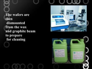
- 12. The wafers are then dismounted from the wax and graphite beam to prepare for cleaning
- 13. After cleaning, the wafers are wax-mounted to a lapping machine . After lapping, the wafers are dismounted on a hot plate, rinsed in a soap solution, and wiped dry.
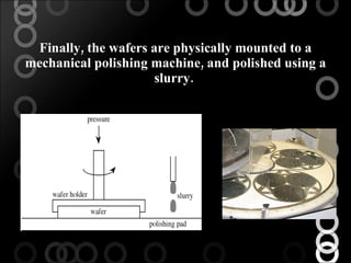
- 14. Finally, the wafers are physically mounted to a mechanical polishing machine, and polished using a slurry.
- 15. Cleaning During the processes described above, semiconductor wafers are subjected to physical handling that leads to significant contamination. Possible sources of physical contamination include: airborne bacteria, grease and wax from cutting oils and physical handling, abrasive particulates from lapping, grinding or sawing operations, plasticizers which are derived from containers and wrapping in which the wafers are handled and shipped.
- 16. Oxidation What is Wafer Oxidation? Oxidation is a process of formation of oxide layer on a wafer. Importance of Wafer Oxidation Surface Passivation Doping Barrier Surface Dielectric
- 17. Surface Passivation - Protection from contamination and physical surface scratches during fabrication process. Doping Barrier - Blocks the dopants from reaching the Si surface of the wafer. Surface Dielectric - SiO 2 layer prevents shorting of metal layer to underlying metal.
- 18. Types of Oxidation Thermal Oxidation Chemical reaction of thermal oxide growth Si (solid) + O 2 (gas) SiO 2 (solid) Temperature Ranges from 800 – 1200 C Si wafer placed in a furnace exposed to oxygen gas. Can be Wet or Dry Oxidation Si (solid) + O 2 (gas) SiO 2 (solid) (dry oxidation) or Si (solid) + 2H 2 O (gas) SiO 2 (solid) + 2H 2 (gas) (wet oxidation)
- 19. High Pressure Oxidation High pressure oxidation has a faster oxidation rate than thermal oxidation Higher dielectric strength than thermal oxidation High pressure system similar to conventional horizontal tube furnace Oxidant is pumped into the tube at pressure 10-25 atm 1 atm causes temperature drop of 30 C
- 20. Two Types of Furnaces
- 21. Photolithography The process of transferring geometric shapes on a mask to the surface of a silicon wafer Steps in Photolithographic process Wafer cleaning Barrier layer information Photoresist application Soft baking Mask alignment Exposure and development Hard baking
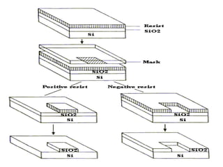
- 22. Wafer Cleaning, Barrier Formation and Photoresist Application Wafers are chemically cleaned to remove particles and impurities Silicon Dioxide is applied to the surface of the wafer as a barrier layer Photoresist is applied to the surface of the wafer by a technique known as “Spin Coating”
- 23. Positive and Negative Photoresist Positive Photoresist the resist is exposed with UV light wherever the underlying material is to be removed Exposure to the UV light changes the chemical structure that it becomes more soluble in the developer Negative Photoresist Exposure to UV light causes resist to be polymerized Resulting masks used for negative photoresists contain “photographic negative” of pattern to be transferred
- 25. Soft-Baking Step during which almost all of the solvents are removed from the photoresist coating The photoresist coatings become photosensitive, or imageable, only after softbaking
- 26. Mask Alignment and Exposure A mask or "photomask" is a square glass plate with a patterned emulsion of metal film on one side Once the mask has been accurately aligned with the pattern on the wafer's surface, the photoresist is exposed through the pattern on the mask with a high intensity ultraviolet light
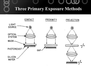
- 27. Three Primary Exposure Methods
- 28. Contact and Proximity Printing The resist-coated silicon wafer is brought into physical contact with the glass photomask The photoresist is exposed with UV light while the wafer is in contact position with the mask
- 29. Projection Printing Avoids mask damage entirely An image of the patterns on the mask is projected onto the resist-coated wafer Small image field is scanned or stepped over the surface of the wafer
- 31. Development At low-exposure energies, the negative resist remains completely soluble in the developer solution. As the exposure is increased above a threshold energy Et, more of the resist film remains after development. At exposures two or three times the threshold energy, very little of the resist film is dissolved. For positive resists, the resist solubility in its developer is finite even at zero-exposure energy. The solubility gradually increases until, at some threshold, it becomes completely soluble. These curves are affected by all the resist processing variables: initial resist thickness, prebake conditions, developer chemistry, developing time, and others
- 32. Hard-Baking Hard-baking is the final step in the photolithographic process. This step is necessary in order to harden the photoresist and improve adhesion of the photoresist to the wafer surface.
- 33. Doping The operation of semiconductor devices requires that specific regions of the substrate be doped n-type of p-type with specific dopant concentrations. Diffusion Ion Implantation
- 34. Diffusion Movement of a chemical species from an area of high concentration to an area of lower concentration. Alter the type and level of conductivity of semiconductor materials. Types of Diffusion: Gas-state Diffusion Liquid-state Diffusion Solid-state Diffusion
- 35. Major Steps of Diffusion: Deposition/Predeposition A flux of impurities continuously arrives at the surface of the substrate. Drive-In / Oxidation A thin layer of the impurity material is deposited on the substrate.
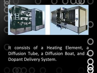
- 36. Typical Diffusion System It consists of a Heating Element, a Diffusion Tube, a Diffusion Boat, and a Dopant Delivery System.
- 37. Variables in Deposition: Surface Concentration Diffusivity Time of Diffusion Junction Depth Quantity of Atoms Diffused
- 38. Fick’s Laws Fick’s First Law An equation describing the flow of an impurity in a substance. Fick’s Second Law The concentration gradient of an impurity in a finite volume of material decreases with time.
- 39. Ion Implantation Process by which ions of a material can be implanted into another solid. An impurity is introduced into the semiconductor by creating ions of the impurity.
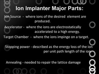
- 41. Ion Source - where ions of the desired element are produced. Accelerator - where the ions are electrostatically accelerated to a high energy. Target Chamber - where the ions impinge on a target. Ion Implanter Major Parts: Stopping power - described as the energy loss of the ion per unit path length of the ion. Annealing - needed to repair the lattice damage
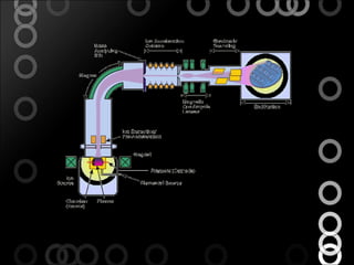
- 42. Ion Implantation Setup with Mass Separator
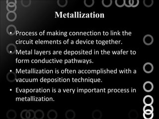
- 43. Metallization Process of making connection to link the circuit elements of a device together. Metal layers are deposited in the wafer to form conductive pathways. Metallization is often accomplished with a vacuum deposition technique. Evaporation is a very important process in metallization.
- 44. The evaporation process Step 1 – the solid metal must be changed into a gaseous vapor by heating. Step 2 – the gaseous vapor must be transported to the substrate containing the wafer. Step 3 – the gas must condense onto the substrate to form a metallic layer .
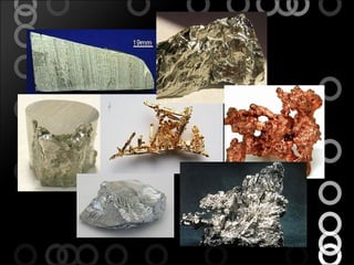
- 45. Metals used in metallization Aluminum Nickel Chromium Gold Germanium Copper Silver Titanium Tungsten Platinum Tantalum
- 47. Filament Evaporation Also called resistive evaporation It is the simplest method of metal deposition. It is accomplished by gradually heating the filament of a metal to be evaporated. The metal is placed on a “bell jar”, in which a filament is heated by increasing the current through the filament.
- 48. Flash Evaporation A ceramic material, usually in a form of a bar, is heated by thermal resistance. Metal wires are continuously passed to the heated ceramic material to be evaporated. After the evaporation, the metal vapor is deposited on the substrate.
- 49. Electron-Beam Evaporation Electron beams are used to evaporate the material to be used. The benefits of this technique is speed and low contamination. The metal is kept in a water-cooled crucible while being exposed to the e-beam causing it to vaporize and then condense immediately on to the substrate.
- 50. Sputtering Commonly used technique in IC metallization. It is popular because the adhesion of the deposited metals is excellent. Inert gases (such as argon) are ionized in an electric field. The ionized atoms of the gas are drawn to one place called the target.
- 51. The target is comprised of metal used for deposition. As the ions strike the target, they dislodge, or “sputter”, the metal atoms. The dislodge atoms are then deposited on the substrate facing the target to form the desired metallic layer.
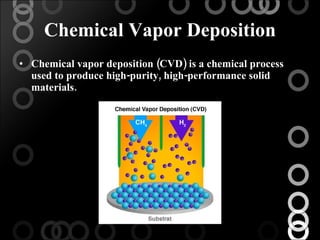
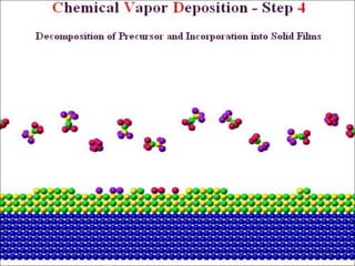
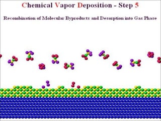
- 52. Chemical Vapor Deposition Chemical vapor deposition (CVD) is a chemical process used to produce high-purity, high-performance solid materials.
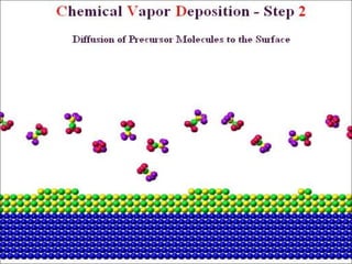
- 53. Step 1: Vaporization and Transport of
- 58. Applications of CVD: integrated circuits optoelectronic devices and sensors catalysts micro machines fine metal ceramic powders protective coatings
- 59. Wafer Testing Done during the final steps of a semiconductor device fabrication. Devices are subjected to a variety of tests to determine if they function properly. Test program Other terms for wafer test: Wafer Sort (WS) Wafer Final Test (WFT) Electronic Die Sort (EDS) Circuit Probe (CP)
- 60. Kinds of Test Probe Test The wafer testing is performed by a piece of test equipment called a wafer prober. The wafer prober also exercises any test circuitry on the wafer scribe lines. Electrical Testing the identification and segregation of electrical failures from a population of devices. An electrical failure is any unit that does not meet the electrical specifications defined for the device. test is done on an Automatic Test Equipment (ATE) which consists of a tester and a handler. Consist of several test blocks which tests the DUT for a certain parameter
- 61. 2 verisions of test program: Production version Quality assurance version 2 types of test blocks in the test program: Parametric Functional Burn-in an electrical stress test that employs voltage and temperature to accelerate the electrical failure of a device. simulates the operating life of the device. 2 kinds of burn-ins: Early life failure (ELF) monitor burn-in High Temperature Operating Life (HTOL) Test
- 62. Strip/Matrix Testing the process wherein semiconductor devices are electrically tested while they are still in their lead frame strips (before they are singulated). a relatively new test process that is not applicable to all semiconductor packages. This is because it inserts the test process even before the devices are sigulated wherein what usually happens is that the singulation occurs first before the test. Benefits of Split Testing: Solves the difficulties of handling very small packages after these have been singulated. With this kind of test, significant reduction in test cycle time.
- 63. Wafer Evaluation
- 64. Marking The process of putting identification, traceability, and distinguishing marks on the package of an IC. 2 marking processes: Ink Marking Pad Printing Most common ink marking process for semiconductor products is pad printing. Consists of transferring an ink pattern from the plate, which is a flat block with pattern depressions that are filled with ink, to the package, using a silicone rubber stamp pad. Follows certain steps. Laser Marking
- 65. Common marking failure missing mark missing character misoriented mark wrong mark format misplaced mark mark permanency failure inadequate mark contrast
- 66. Packaging Tape & Reel A process of packing surface mount devices (SMD's) by loading them into individual pockets comprising what is known as a pocket tape or carrier tape. Dry Packing The process of putting moisture-sensitive plastic surface-mount devices in moisture-resistant bags or moisture barrier bags to prevent them from absorbing moisture from the atmosphere.
- 67. Boxing & Labelling The process of packing the lot in its box and attaching the required lot identification labels for storage in the finished goods warehouse or shipment to the customer.


