GRAPHENE PRESENTATION
•
14 likes•11,589 views

For free download Subscribe to https://www.youtube.com/channel/UCTfiZ8qwZ_8_vTjxeCB037w and Follow https://www.instagram.com/fitrit_2405/ then please contact +91-9045839849 over WhatsApp. Graphene Presentation
Report
Share

GRAPHENE PRESENTATION
- 1. Amity School of Engineering & Technology Graphene: From fundamental to future applications Aman Gupta B.Tech ECE 3 Sem
- 2. Amity School of Engineering & Technology Content Introduction to graphene. Preparation and characterization graphene Potential application of graphene Conclusions
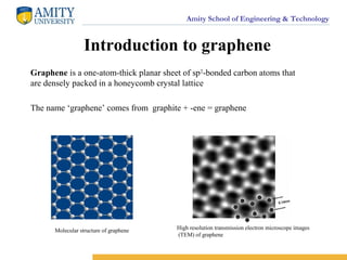
- 3. Amity School of Engineering & Technology Graphene is a one-atom-thick planar sheet of sp2 -bonded carbon atoms that are densely packed in a honeycomb crystal lattice The name ‘graphene’ comes from graphite + -ene = graphene High resolution transmission electron microscope images (TEM) of graphene Introduction to graphene Molecular structure of graphene
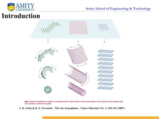
- 4. Amity School of Engineering & Technology A. K. Geim & K. S. Novoselov. The rise of graphene. Nature Materials Vol . 6 ,183-191 (2007). Introduction
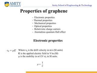
- 5. Amity School of Engineering & Technology - Electronic properties - Thermal properties - Mechanical properties - Optical properties - Relativistic charge carriers - Anomalous quantum Hall effect Properties of graphene Electronic properties Where υd is the drift velocity in m/s (SI units) E is the applied electric field in V/m (SI) µ is the mobility in m2 /(V·s), in SI units.
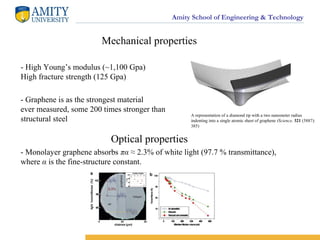
- 6. Amity School of Engineering & Technology - High Young’s modulus (~1,100 Gpa) High fracture strength (125 Gpa) - Monolayer graphene absorbs πα ≈ 2.3% of white light (97.7 % transmittance), where α is the fine-structure constant. Mechanical properties Optical properties A representation of a diamond tip with a two nanometer radius indenting into a single atomic sheet of graphene (Science, 321 (5887): 385) - Graphene is as the strongest material ever measured, some 200 times stronger than structural steel
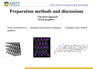
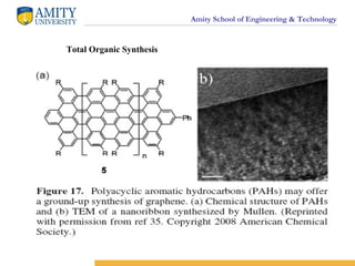
- 7. Amity School of Engineering & Technology Preparation of graphene Preparation methods Top-down approach (From graphite) Bottom up approach (from carbon precursors) - By chemical vapour deposition (CVD) of hydrocarbon - By epitaxial growth on electrically insulating surfaces such as SiC - Total Organic Synthesis - Micromechanical exfoliation of graphite (Scotch tape or peel-off method) - Creation of colloidal suspensions from graphite oxide or graphite intercalation compounds (GICs)
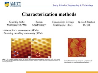
- 8. Amity School of Engineering & Technology Characterization methods Scanning Probe Microscopy (SPM): - Atomic force microscopes (AFMs) - Scanning tunneling microscopy (STM) Raman Spectroscopy Transmission electron Microscopy (TEM) X-ray diffraction (XRD) Atomic force microscopy images of a graphite oxide film deposited by Langmuir-Blodgett assembly
- 9. Amity School of Engineering & Technology Top-down approach (From graphite) Graphite oxide methodGraphite intercalation compoundDirect exfoliation of graphite Preparation methods and discussions
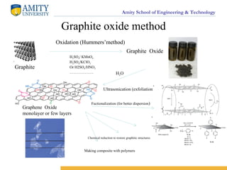
- 10. Amity School of Engineering & Technology Graphite oxide method Graphite Oxidation (Hummers’method) H2SO4/ KMnO4 H2SO4/KClO3 Or H2SO4/HNO3 ………………. H2O Ultrasonication (exfoliation) Graphite Oxide Graphene Oxide monolayer or few layers Fuctionalization (for better dispersion) Making composite with polymers Chemical reduction to restore graphitic structures
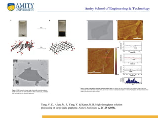
- 11. Amity School of Engineering & Technology Tung, V. C., Allen, M. J., Yang, Y. & Kaner, R. B. High-throughput solution processing of large-scale graphene. Nature Nanotech. 4, 25–29 (2008).
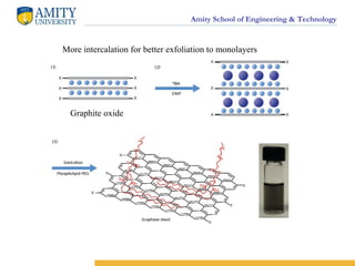
- 12. Amity School of Engineering & Technology More intercalation for better exfoliation to monolayers Graphite oxide
- 13. Amity School of Engineering & Technology Total Organic Synthesis
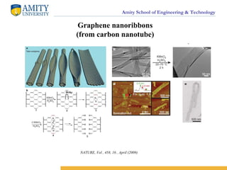
- 14. Amity School of Engineering & Technology Graphene nanoribbons (from carbon nanotube) NATURE, Vol , 458, 16 , April (2009)
- 15. Amity School of Engineering & Technology Potential application of graphene - Single molecule gas detection - Graphene transistors - Integrated circuits - Transparent conducting electrodes for the replacement of ITO - Ultracapacitors - Graphene biodevices - Reinforcement for polymer nanocomposites: Electrical, thermally conductive nanocomposites, antistatic coating, transparent conductive composites.
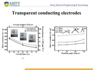
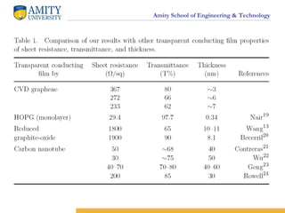
- 16. Amity School of Engineering & Technology Transparent conducting electrodes
- 17. Amity School of Engineering & Technology
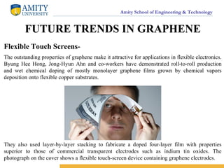
- 18. Amity School of Engineering & Technology FUTURE TRENDS IN GRAPHENE Flexible Touch Screens- The outstanding properties of graphene make it attractive for applications in flexible electronics. Byung Hee Hong, Jong-Hyun Ahn and co-workers have demonstrated roll-to-roll production and wet chemical doping of mostly monolayer graphene films grown by chemical vapors deposition onto flexible copper substrates. They also used layer-by-layer stacking to fabricate a doped four-layer film with properties superior to those of commercial transparent electrodes such as indium tin oxides. The photograph on the cover shows a flexible touch-screen device containing graphene electrodes.
- 19. Amity School of Engineering & Technology Magnetism and Graphene- Given the great versatility of graphene’s properties and especially the ability to control many of its characteristics by external electric field (gate voltage), graphene has a potential to become an excellent material for spintronics. Our current efforts concentrate on ‘making graphene magnetic’ by introducing point defects, such as vacancies or adatoms. We have already demonstrated that vacancies in graphene act as individual magnetic moments and lead to pronounced paramagnetism.
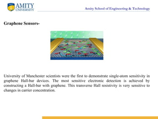
- 20. Amity School of Engineering & Technology Graphene Sensors- University of Manchester scientists were the first to demonstrate single-atom sensitivity in graphene Hall-bar devices. The most sensitive electronic detection is achieved by constructing a Hall-bar with graphene. This transverse Hall resistivity is very sensitive to changes in carrier concentration.
- 21. Amity School of Engineering & Technology CONCLUSION Graphene has an interesting history, but many now wonder about its future. The subject of considerable scholarly debate, it does seem reasonable to assert a few things looking ahead: First, the quality and availability of “synthetic” graphene will continue to improve. Whether high quality material comes in the form of an alternative chemical route to the complete exfoliation of graphite or from optimization of the thermal processes required for substrate-based methods, there is no sign that synthetic techniques are nearing their upper limit. This means that device engineers will have ample access to improved materials for developing novel structures and finding ways to integrate graphene into present-day electronic devices.
- 22. Amity School of Engineering & Technology Second, chemical modification of graphene’s basal plane or its edges will substantially influence graphene-based devices. For electronic applications, one can imagine the attachment of functional groups aimed at self-assembly of simple circuits or the incorporation of chemical dopants to limit leakage current under zero gate bias. For sensors, lock and-key type binding sites could provide selective sensitivity to a wide variety of analytes. These might include chemical warfare agents or even biological species. Third, industrial use of graphene as a transparent conductor could have huge implications for the solar industry. As synthetic routes improve, the prospect of replacing ITO with a low-cost carbon-based coating seems feasible. This would not only remove significant uncertainty about the availability and cost of indium but also enable non evaporative roll-to roll processing of transparent conductors.
- 23. Amity School of Engineering & Technology