AVR_Course_Day1 basic electronics
•
259 likes•32,534 views

This is a microcontroller course for atmega328 (the chip used in Arduino Uno) explained very simply .
Report
Share
Related slideshows


AVR_Course_Day1 basic electronics
- 1. Basic Electronics Eng. Mohamed Loay Ali Eng:Mohamed Loay Ali Basic Electronics 1
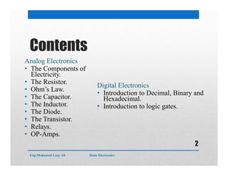
- 2. Contents Analog Electronics • The Components of Electricity. • The Resistor. • Ohm’s Law. • The Capacitor. • The Inductor. • The Diode. • The Transistor. • Relays. • OP-Amps. Digital Electronics • Introduction to Decimal, Binary and Hexadecimal. • Introduction to logic gates. Eng:Mohamed Loay Ali Basic Electronics 2
- 3. Analogue Electronics The Components of Electricity. • The Resistor. • The Capacitor. • The Inductor. • The Diode. • The Transistor. • Relays. • OP-Amps. Eng:Mohamed Loay Ali Basic Electronics 3
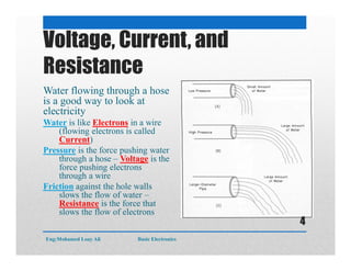
- 4. Voltage, Current, and Resistance Water flowing through a hose is a good way to look at electricity Water is like Electrons in a wire (flowing electrons is called Current) Pressure is the force pushing water through a hose – Voltage is the force pushing electrons through a wire Friction against the hole walls slows the flow of water – Resistance is the force that slows the flow of electrons Eng:Mohamed Loay Ali Basic Electronics 4
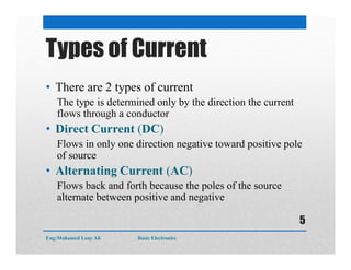
- 5. Types of Current • There are 2 types of current The type is determined only by the direction the current flows through a conductor • Direct Current (DC) Flows in only one direction negative toward positive pole of source • Alternating Current (AC) Flows back and forth because the poles of the source alternate between positive and negative Eng:Mohamed Loay Ali Basic Electronics 5
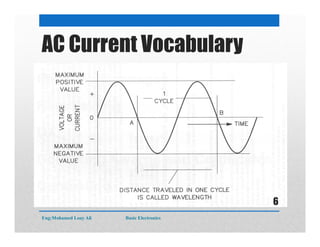
- 6. AC Current Vocabulary Eng:Mohamed Loay Ali Basic Electronics 6
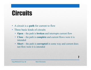
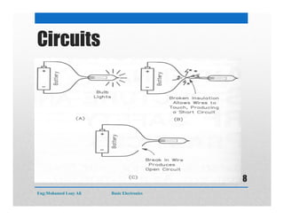
- 7. Circuits • A circuit is a path for current to flow • Three basic kinds of circuits • Open – the path is broken and interrupts current flow • Close – the path is complete and current flows were it is intended • Short – the path is corrupted in some way and current does not flow were it is intended Eng:Mohamed Loay Ali Basic Electronics 7
- 8. Circuits Eng:Mohamed Loay Ali Basic Electronics 8
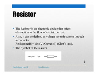
- 9. Resistor • The Resistor is an electronic device that offers obstruction to the flow of electric current. • Also, it can be defined as voltage per unit current through a conductor Resistance(R)= Volt(V)/Current(I) (Ohm’s law). • The Symbol of the resistor Eng:Mohamed Loay Ali Basic Electronics 9
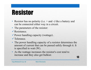
- 10. Resistor • Resistor has no polarity (i.e. + and -) like a battery and can be connected either way in a circuit. • The parameters of the resistor: Resistance. Power handling capacity (wattage) . Tolerance. • The power handling capacity of a resistor determines the amount of current that can be passed safely through it. It is specified in watt (W). • As the wattage increases the resistor's cost tend to increase and they also get bulkier. Eng:Mohamed Loay Ali Basic Electronics 10
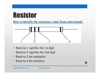
- 11. Resistor How to identify the resistance value from color bands: • Band no.1 signifies the 1st digit • Band no.2 signifies the 2nd digit • Band no.3 the multiplier. • Band no.4 the tolerance Eng:Mohamed Loay Ali Basic Electronics 11
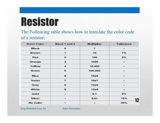
- 12. Resistor The Following table shows how to translate the color code of a resistor: Eng:Mohamed Loay Ali Basic Electronics 12
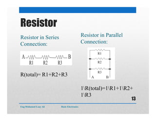
- 13. Resistor Resistor in Series Connection: R(total)= R1+R2+R3 Resistor in Parallel Connection: 1R(total)=1R1+1R2+ 1R3 Eng:Mohamed Loay Ali Basic Electronics 13
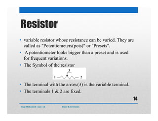
- 14. Resistor • variable resistor whose resistance can be varied. They are called as "Potentiometers(pots)" or "Presets". • A potentiometer looks bigger than a preset and is used for frequent variations. • The Symbol of the resistor • The terminal with the arrow(3) is the variable terminal. • The terminals 1 & 2 are fixed. Eng:Mohamed Loay Ali Basic Electronics 14
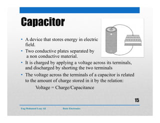
- 15. Capacitor • A device that stores energy in electric field. • Two conductive plates separated by a non conductive material. • It is charged by applying a voltage across its terminals, and discharged by shorting the two terminals • The voltage across the terminals of a capacitor is related to the amount of charge stored in it by the relation: Voltage = Charge/Capacitance Eng:Mohamed Loay Ali Basic Electronics 15
- 16. Capacitor Types of Capacitor: 1. Non-electrolytic capacitors are non-polarized, i.e they can be connected either way in a circuit without having to worry about + &-. Its value ranges between about a few pF to as high as 1 uF. 2. Electrolytic capacitors are polarized and they are supposed to be connected in a specific way in the circuit. Its value ranges between 1 uF and upwards up to about 4700uF. Eng:Mohamed Loay Ali Basic Electronics 16
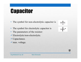
- 17. Capacitor • The symbol for non-electrolytic capacitor is • The symbol for electrolytic capacitor is • The parameters of the resistor: Electrolytic/non-electrolytic. Capacitance. max. voltage. Eng:Mohamed Loay Ali Basic Electronics 17
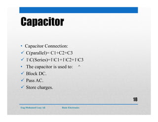
- 18. Capacitor • Capacitor Connection: C(parallel)= C1+C2+C3 1C(Series)=1C1+1C2+1C3 • The capacitor is used to: ^ Block DC. Pass AC. Store charges. Eng:Mohamed Loay Ali Basic Electronics 18
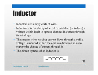
- 19. Inductor • Inductors are simply coils of wire. • Inductance is the ability of a coil to establish (or induce) a voltage within itself to oppose changes in current through its windings. • That means when varying current flows through a coil, a voltage is induced within the coil in a direction so as to oppose the change of current through it • The circuit symbol of an inductor is Eng:Mohamed Loay Ali Basic Electronics 19
- 20. Inductor • Inductance is measured in Henry(s). • A Henry is a measure of the intensity of the magnetic field that is produced. • Typical inductor values used in electronics are in the range of milli Henry (1/1000) and micro Henry (1/1,000,000) Eng:Mohamed Loay Ali Basic Electronics 20
- 21. Inductor • Like capacitors, inductors temporarily store energy. • Unlike capacitors: • Inductors store energy in a magnetic field, not an electric field. • When the source of electrons is removed, the magnetic field collapses immediately. Eng:Mohamed Loay Ali Basic Electronics 21
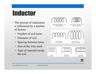
- 22. Inductor • The amount of inductance is influenced by a number of factors: • Number of coil turns. • Diameter of coil. • Spacing between turns. • Size of the wire used. • Type of material inside the coil. Eng:Mohamed Loay Ali Basic Electronics 22
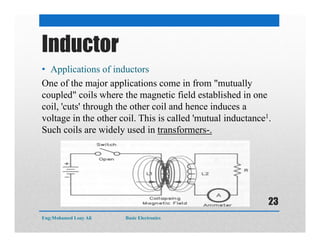
- 23. Inductor • Applications of inductors One of the major applications come in from "mutually coupled" coils where the magnetic field established in one coil, 'cuts' through the other coil and hence induces a voltage in the other coil. This is called 'mutual inductance1. Such coils are widely used in transformers-. Eng:Mohamed Loay Ali Basic Electronics 23
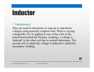
- 24. Inductor • Transformers: They are used in electronics to step-up or step-down voltages using mutually coupled coils. When a varying voltage(like AC) is applied to one of the coils of the transformer(called the Primary winding), a voltage is 'induced' in the other coil due to mutual inductance. The second coil in which the voltage is induced is called the Secondary winding. Eng:Mohamed Loay Ali Basic Electronics 24
- 25. Inductor • Transformers are specified bythe following: Primary and secondary voltages. Current rating. • For example, a 230V /12-0-12V and 1A transformer means, the primary voltage is 230V and secondary voltages are 12V,0V,12V of the 3 tapings and can supply a maximum of 1A (this is the root-mean-square , rms value). If you want to 12V from the transformer, then you can use the center tap and either of the other 2 end terminals. Eng:Mohamed Loay Ali Basic Electronics 25
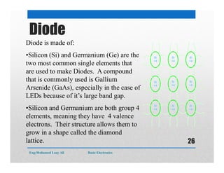
- 26. Diode Diode is made of: •Silicon (Si) and Germanium (Ge) are the two most common single elements that are used to make Diodes. A compound that is commonly used is Gallium Arsenide (GaAs), especially in the case of LEDs because of it’s large band gap. •Silicon and Germanium are both group 4 elements, meaning they have 4 valence electrons. Their structure allows them to grow in a shape called the diamond lattice. Si +4 Si +4 Si +4 Si +4 Si +4 Si +4 Si +4 Si +4 Si +4 Eng:Mohamed Loay Ali Basic Electronics 26
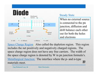
- 27. Steady State P n - - - - - - - - - - - - - - - - - - - - + + + + + + + + + + + + + + + + + + + + Na Nd Metallurgical Junction Space Charge Regionionized acceptors ionized donors E-Field ++ _ _ h+ drift h+ diffusion e- diffusion e- drift= == = When no external source is connected to the pn junction, diffusion and drift balance each other out for both the holes and electrons Space Charge Region: Also called the depletion region. This region includes the net positively and negatively charged regions. The space charge region does not have any free carriers. The width of the space charge region is denoted by W in pn junction formula’s. Metallurgical Junction: The interface where the p- and n-type materials meet. Diode Eng:Mohamed Loay Ali Basic Electronics 27
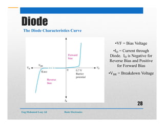
- 28. Diode The Diode Characteristics Curve •VF = Bias Voltage •ID = Current through Diode. ID is Negative for Reverse Bias and Positive for Forward Bias •VBR = Breakdown Voltage Eng:Mohamed Loay Ali Basic Electronics 28
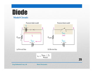
- 29. Diode Model Circuit: Eng:Mohamed Loay Ali Basic Electronics 29
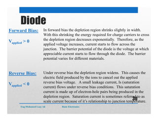
- 30. Forward Bias: In forward bias the depletion region shrinks slightly in width. With this shrinking the energy required for charge carriers to cross the depletion region decreases exponentially. Therefore, as the applied voltage increases, current starts to flow across the junction. The barrier potential of the diode is the voltage at which appreciable current starts to flow through the diode. The barrier potential varies for different materials. Reverse Bias: Under reverse bias the depletion region widens. This causes the electric field produced by the ions to cancel out the applied reverse bias voltage. A small leakage current, Is (saturation current) flows under reverse bias conditions. This saturation current is made up of electron-hole pairs being produced in the depletion region. Saturation current is sometimes referred to as scale current because of it’s relationship to junction temperature. Vapplied > 0 Vapplied < 0 Diode Eng:Mohamed Loay Ali Basic Electronics 30
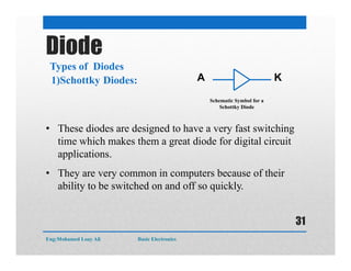
- 31. Diode Types of Diodes 1)Schottky Diodes: • These diodes are designed to have a very fast switching time which makes them a great diode for digital circuit applications. • They are very common in computers because of their ability to be switched on and off so quickly. A K Schematic Symbol for a Schottky Diode Eng:Mohamed Loay Ali Basic Electronics 31
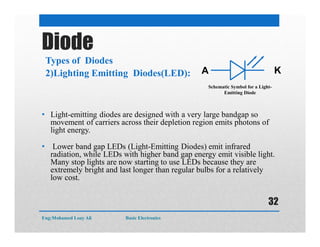
- 32. Diode • Light-emitting diodes are designed with a very large bandgap so movement of carriers across their depletion region emits photons of light energy. • Lower band gap LEDs (Light-Emitting Diodes) emit infrared radiation, while LEDs with higher band gap energy emit visible light. Many stop lights are now starting to use LEDs because they are extremely bright and last longer than regular bulbs for a relatively low cost. 2)Lighting Emitting Diodes(LED): A Schematic Symbol for a Light- Emitting Diode K Types of Diodes Eng:Mohamed Loay Ali Basic Electronics 32
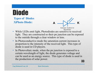
- 33. Diode • While LEDs emit light, Photodiodes are sensitive to received light. They are constructed so their pn junction can be exposed to the outside through a clear window or lens. • In Photoconductive mode the saturation current increases in proportion to the intensity of the received light. This type of diode is used in CD players. • In Photovoltaic mode, when the pn junction is exposed to a certain wavelength of light, the diode generates voltage and can be used as an energy source. This type of diode is used in the production of solar power. Types of Diodes 3)Photo Diode: KA Schematic Symbols for Photodiodes Eng:Mohamed Loay Ali Basic Electronics 33
- 34. Diode • Photo diode diagram: • The Circuit: Eng:Mohamed Loay Ali Basic Electronics 34
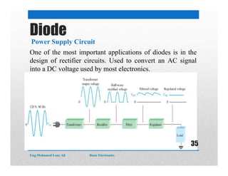
- 35. Power Supply Circuit Diode One of the most important applications of diodes is in the design of rectifier circuits. Used to convert an AC signal into a DC voltage used by most electronics. Eng:Mohamed Loay Ali Basic Electronics 35
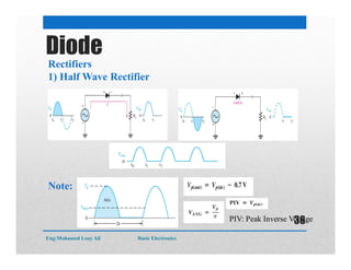
- 36. Rectifiers 1) Half Wave Rectifier Diode Note: PIV: Peak Inverse Voltage Eng:Mohamed Loay Ali Basic Electronics 36
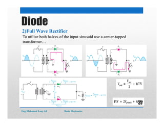
- 37. To utilize both halves of the input sinusoid use a center-tapped transformer… Diode 2)Full Wave Rectifier Eng:Mohamed Loay Ali Basic Electronics 37
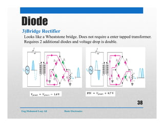
- 38. 3)Bridge Rectifier Diode Looks like a Wheatstone bridge. Does not require a enter tapped transformer. Requires 2 additional diodes and voltage drop is double. Eng:Mohamed Loay Ali Basic Electronics 38
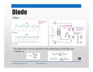
- 39. Diode Filter The ripple factor (r)is an indication of the effectiveness of the filter and is defined as Eng:Mohamed Loay Ali Basic Electronics 39
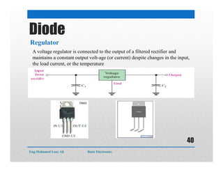
- 40. Diode Regulator A voltage regulator is connected to the output of a filtered rectifier and maintains a constant output volt-age (or current) despite changes in the input, the load current, or the temperature Eng:Mohamed Loay Ali Basic Electronics 40
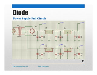
- 41. Diode Power Supply Full Circuit Eng:Mohamed Loay Ali Basic Electronics 41
- 42. Transistor (BJT) Structure: Eng:Mohamed Loay Ali Basic Electronics 42
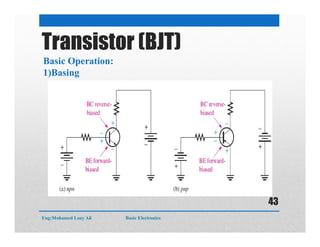
- 43. Transistor (BJT) Basic Operation: 1)Basing Eng:Mohamed Loay Ali Basic Electronics 43
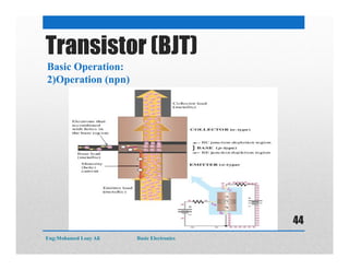
- 44. Basic Operation: 2)Operation (npn) Transistor (BJT) Eng:Mohamed Loay Ali Basic Electronics 44
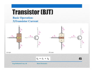
- 45. Basic Operation: 3)Transistor Current Transistor (BJT) Eng:Mohamed Loay Ali Basic Electronics 45
- 46. • DC Beta ( DC) : The dc current gain of a transistor is the ratio of the dc collector current (IC) to the dc base current (IB) and is designated dc beta( beta=ICIB) range from less than 20 to 200 or higher. • DC alpha : The ratio of the dc collector current (IC) to the dc emitter current (IE) (alpha=ICIE) range from 0.95 to 0.99 or greater, always less than 1. Important Parameters: Transistor (BJT) Eng:Mohamed Loay Ali Basic Electronics 46
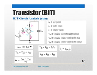
- 47. BJT Circuit Analysis (npn): Transistor (BJT) Eng:Mohamed Loay Ali Basic Electronics 47
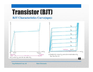
- 48. BJT Characteristics Curve(npn): Transistor (BJT) Eng:Mohamed Loay Ali Basic Electronics 48
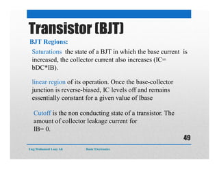
- 49. BJT Regions: Transistor (BJT) Saturations the state of a BJT in which the base current is increased, the collector current also increases (IC= bDC*IB). linear region of its operation. Once the base-collector junction is reverse-biased, IC levels off and remains essentially constant for a given value of Ibase Cutoff is the non conducting state of a transistor. The amount of collector leakage current for IB= 0. Eng:Mohamed Loay Ali Basic Electronics 49
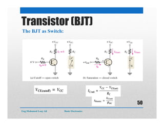
- 50. The BJT as Switch: Transistor (BJT) Eng:Mohamed Loay Ali Basic Electronics 50
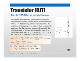
- 51. The BJT(2N3904) as Switch Example: Transistor (BJT) The LED in 30 mA to emit a sufficient level of light. Therefore,the collector current should be approximately 30 mA. For the following circuit values,determine the amplitude of the square wave input voltage necessary to make sure that the transistor saturates. Use double the minimum value of base current as a safety margin to ensure saturation. VCC 9 V, VCE(sat) 0.3 V, RC 220 Æ, RB 3.3 kÆ, bDC =50, and VLED 1.6 =V. Eng:Mohamed Loay Ali Basic Electronics 51
- 52. The Photo transistor: Transistor (BJT) In a phototransisto rthe base current is produced when light strikes the photosensitive semiconductor base region. Eng:Mohamed Loay Ali Basic Electronics 52
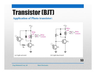
- 53. Application of Photo transistor: Transistor (BJT) Eng:Mohamed Loay Ali Basic Electronics 53
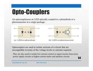
- 54. Opto-Couplers An optocoupleruses an LED optically coupled to a photodiode or a phototransistor in a single package. Optocouplers are used to isolate sections of a circuit that are incompatible in terms of the voltage levels or currents required. They are also used to isolate low-current control or signal circuits from noisy power supply circuits or higher-current motor and machine circuits Eng:Mohamed Loay Ali Basic Electronics 54
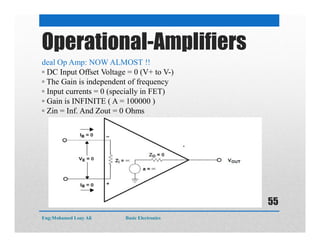
- 55. Operational-Amplifiers deal Op Amp: NOW ALMOST !! ▫ DC Input Offset Voltage = 0 (V+ to V-) ▫ The Gain is independent of frequency ▫ Input currents = 0 (specially in FET) ▫ Gain is INFINITE ( A = 100000 ) ▫ Zin = Inf. And Zout = 0 Ohms Eng:Mohamed Loay Ali Basic Electronics 55
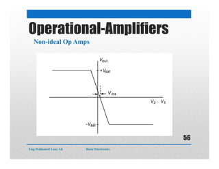
- 56. Operational-Amplifiers Non-ideal Op Amps Eng:Mohamed Loay Ali Basic Electronics 56
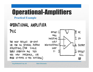
- 57. Operational-Amplifiers Practical Example Eng:Mohamed Loay Ali Basic Electronics 57
- 58. Operational-Amplifiers Practical Example Eng:Mohamed Loay Ali Basic Electronics 58
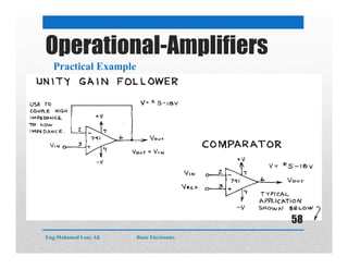
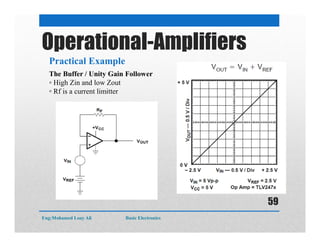
- 59. Operational-Amplifiers Practical Example The Buffer / Unity Gain Follower ▫ High Zin and low Zout ▫ Rf is a current limitter Eng:Mohamed Loay Ali Basic Electronics 59
- 60. Operational-Amplifiers Practical Example The Current to Voltage Converter Eng:Mohamed Loay Ali Basic Electronics 60
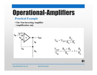
- 61. Operational-Amplifiers Practical Example • The Non-Inverting Amplifier ▫ Amplification only Eng:Mohamed Loay Ali Basic Electronics 61
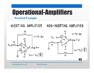
- 62. Operational-Amplifiers Practical Example The Inverting Amplifier ▫ Amplification AND Attenuation Eng:Mohamed Loay Ali Basic Electronics 62
- 63. Operational-Amplifiers Practical Example Eng:Mohamed Loay Ali Basic Electronics 63
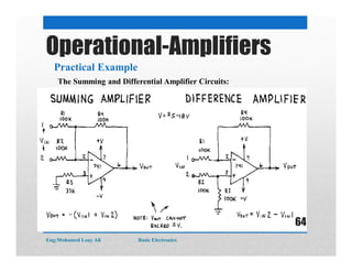
- 64. Operational-Amplifiers Practical Example The Summing and Differential Amplifier Circuits: Eng:Mohamed Loay Ali Basic Electronics 64
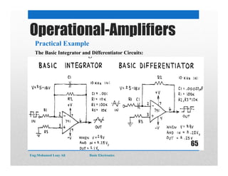
- 65. Operational-Amplifiers Practical Example The Basic Integrator and Differentiator Circuits: Eng:Mohamed Loay Ali Basic Electronics 65
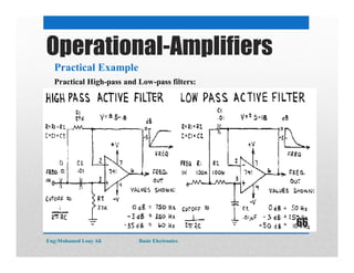
- 66. Operational-Amplifiers Practical Example Practical High-pass and Low-pass filters: Eng:Mohamed Loay Ali Basic Electronics 66
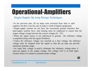
- 67. Operational-Amplifiers Single-Supply Op Amp Design Techniques • In the previous part, all op amps were powered from dual or split supplies, but this is not the case in today’s world of digital equipments. • Single-supply systems do not have the convenient ground reference that dual-supply systems have, thus biasing must be employed to ensure that the output voltage swings between the correct voltages (0 – 5V). • When the signal source is not referenced to ground , the reference voltage is amplified along with the signal (Problem). • Unless the reference voltage was inserted as a bias voltage, the reference voltage must be stripped from the signal so that the op amp can provide maximum dynamic range. • An input bias voltage is used to eliminate the reference voltage when it must not appear in the output voltage. The voltage Vref is in both input circuits, hence it is named a common-mode voltage. Eng:Mohamed Loay Ali Basic Electronics 67
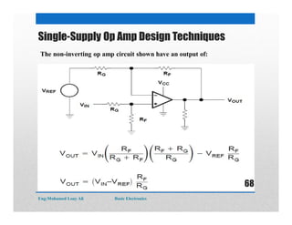
- 68. Single-Supply Op Amp Design Techniques The non-inverting op amp circuit shown have an output of: Eng:Mohamed Loay Ali Basic Electronics 68
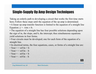
- 69. Single-Supply Op Amp Design Techniques Taking an orderly path to developing a circuit that works the first time starts here; Follow these steps until the equation of the op amp is determined. • A linear op amp transfer function is limited to the equation of a straight line Equation: y = ±mx ± b. • The equation of a straight line has four possible solutions depending upon the sign of m, the slope, and b, the intercept; thus simultaneous equations yield solutions in four forms. • Four circuits must be developed; one for each form of the equation of a straight line. • In electrical terms, the four equations, cases, or forms of a straight line are: ▫ Vout = + mVin + b ▫ Vout = + mVin – b ▫ Vout = – mVin + b ▫ Vout = – mVin – b Eng:Mohamed Loay Ali Basic Electronics 69
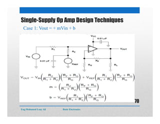
- 70. Single-Supply Op Amp Design Techniques Case 1: Vout = + mVin + b Eng:Mohamed Loay Ali Basic Electronics 70
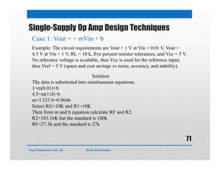
- 71. Single-Supply Op Amp Design Techniques Case 1: Vout = + mVin + b Example: The circuit requirements are Vout = 1 V at Vin = 0.01 V, Vout = 4.5 V at Vin = 1 V, RL = 10 k, five percent resistor tolerances, and Vcc = 5 V. No reference voltage is available, thus Vcc is used for the reference input, thus Vref = 5 V (space and cost savings vs noise, accuracy, and stability). Solution The data is substituted into simultaneous equations. 1=m(0.01)+b 4.5=m(1.0)+b m=3.533 b=0.9646 Select RG=10K and R1=10K Then from m and b equation calculate RF and R2. R2=183.16K but the standard is 180k RF=27.3k and the standard is 27k Eng:Mohamed Loay Ali Basic Electronics 71
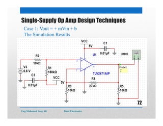
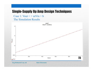
- 72. Single-Supply Op Amp Design Techniques Case 1: Vout = + mVin + b The Simulation Results Eng:Mohamed Loay Ali Basic Electronics 72
- 73. Single-Supply Op Amp Design Techniques Case 1: Vout = + mVin + b The Simulation Results Eng:Mohamed Loay Ali Basic Electronics 73
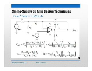
- 74. Single-Supply Op Amp Design Techniques Case 2: Vout = + mVin - b Eng:Mohamed Loay Ali Basic Electronics 74
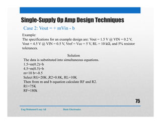
- 75. Single-Supply Op Amp Design Techniques Example: The specifications for an example design are: Vout = 1.5 V @ VIN = 0.2 V, Vout = 4.5 V @ VIN = 0.5 V, Vref = Vcc = 5 V, RL = 10 kΩ, and 5% resistor tolerances. Solution The data is substituted into simultaneous equations. 1.5=m(0.2)+b 4.5=m(0.5)+b m=10 b=-0.5 Select RG=20K ,R2=0.8K, RL=10K Then from m and b equation calculate RF and R2. R1=75K RF=180k Case 2: Vout = + mVin - b Eng:Mohamed Loay Ali Basic Electronics 75
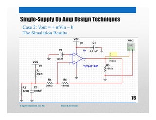
- 76. Single-Supply Op Amp Design Techniques Case 2: Vout = + mVin – b The Simulation Results Eng:Mohamed Loay Ali Basic Electronics 76
- 77. Single-Supply Op Amp Design Techniques Case 2: Vout = + mVin – b The Simulation Results Eng:Mohamed Loay Ali Basic Electronics 77
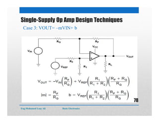
- 78. Single-Supply Op Amp Design Techniques Case 3: VOUT= –mVIN+ b Eng:Mohamed Loay Ali Basic Electronics 78
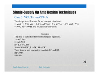
- 79. Single-Supply Op Amp Design Techniques Case 3: VOUT= –mVIN+ b The design specifications for an example circuit are: Vout = 1 V @ Vin = -0.1 V and Vout = 6 V @ Vin = -1 V, Vref = Vcc = 10 V, RL= 100 Ω, and 5% resistor tolerances. Solution The data is substituted into simultaneous equations. 1=m(-0.1)+b 5=m(0.5)+b m=-5.6 b=0.444 Select RG=10K ,R1=2K, RL=10K Then from m and b equation calculate RF and R2. R1=300K RF=56k Eng:Mohamed Loay Ali Basic Electronics 79
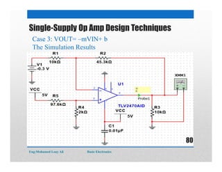
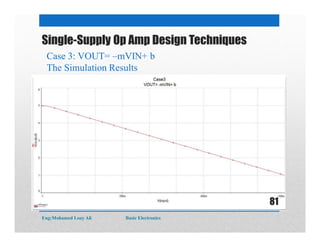
- 80. Single-Supply Op Amp Design Techniques Case 3: VOUT= –mVIN+ bCase 3: VOUT= –mVIN+ b The Simulation Results Eng:Mohamed Loay Ali Basic Electronics 80
- 81. Single-Supply Op Amp Design Techniques Case 3: VOUT= –mVIN+ b The Simulation Results Eng:Mohamed Loay Ali Basic Electronics 81
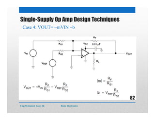
- 82. Single-Supply Op Amp Design Techniques Case 4: VOUT= –mVIN –b Eng:Mohamed Loay Ali Basic Electronics 82
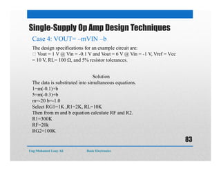
- 83. Single-Supply Op Amp Design Techniques The design specifications for an example circuit are: Vout = 1 V @ Vin = -0.1 V and Vout = 6 V @ Vin = -1 V, Vref = Vcc = 10 V, RL= 100 Ω, and 5% resistor tolerances. Solution The data is substituted into simultaneous equations. 1=m(-0.1)+b 5=m(-0.3)+b m=-20 b=-1.0 Select RG1=1K ,R1=2K, RL=10K Then from m and b equation calculate RF and R2. R1=300K RF=20k RG2=100K Case 4: VOUT= –mVIN –b Eng:Mohamed Loay Ali Basic Electronics 83
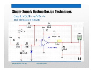
- 84. Single-Supply Op Amp Design Techniques Case 4: VOUT= –mVIN –b The Simulation Results Eng:Mohamed Loay Ali Basic Electronics 84
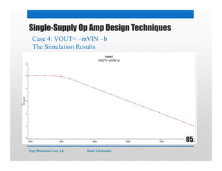
- 85. Single-Supply Op Amp Design Techniques Case 4: VOUT= –mVIN –b The Simulation Results Eng:Mohamed Loay Ali Basic Electronics 85
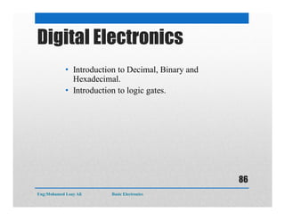
- 86. • Introduction to Decimal, Binary and Hexadecimal. • Introduction to logic gates. Digital Electronics Eng:Mohamed Loay Ali Basic Electronics 86
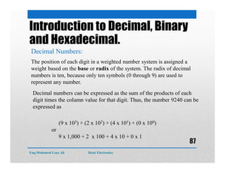
- 87. Introduction to Decimal, Binary and Hexadecimal. Decimal Numbers: The position of each digit in a weighted number system is assigned a weight based on the base or radix of the system. The radix of decimal numbers is ten, because only ten symbols (0 through 9) are used to represent any number. (9 x 10³) + (2 x 10²) + (4 x 101) + (0 x 100) or 9 x 1,000 + 2 x 100 + 4 x 10 + 0 x 1 Decimal numbers can be expressed as the sum of the products of each digit times the column value for that digit. Thus, the number 9240 can be expressed as Eng:Mohamed Loay Ali Basic Electronics 87
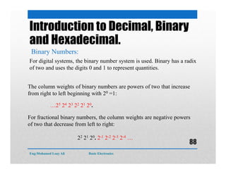
- 88. Introduction to Decimal, Binary and Hexadecimal. Binary Numbers: For digital systems, the binary number system is used. Binary has a radix of two and uses the digits 0 and 1 to represent quantities. The column weights of binary numbers are powers of two that increase from right to left beginning with 20 =1: …25 24 23 22 21 20. For fractional binary numbers, the column weights are negative powers of two that decrease from left to right: 22 21 20. 2-1 2-2 2-3 2-4 … Eng:Mohamed Loay Ali Basic Electronics 88
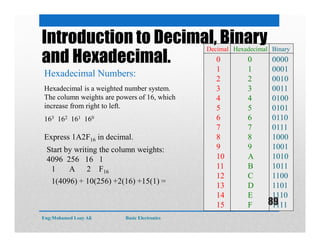
- 89. 1 A 2 F16 Express 1A2F16 in decimal. Start by writing the column weights: 4096 256 16 1 1(4096) + 10(256) +2(16) +15(1) = 0 1 2 3 4 5 6 7 8 9 10 11 12 13 14 15 0 1 2 3 4 5 6 7 8 9 A B C D E F 0000 0001 0010 0011 0100 0101 0110 0111 1000 1001 1010 1011 1100 1101 1110 1111 Decimal Hexadecimal Binary Introduction to Decimal, Binary and Hexadecimal. Hexadecimal Numbers: Hexadecimal is a weighted number system. The column weights are powers of 16, which increase from right to left. 163 162 161 160 Eng:Mohamed Loay Ali Basic Electronics 89
- 90. Introduction to logic gates Not Gate or Inverter Eng:Mohamed Loay Ali Basic Electronics 90
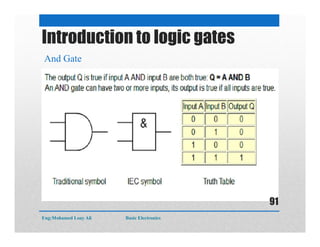
- 91. Introduction to logic gates And Gate Eng:Mohamed Loay Ali Basic Electronics 91
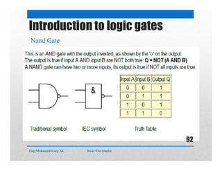
- 92. Introduction to logic gates Nand Gate Eng:Mohamed Loay Ali Basic Electronics 92
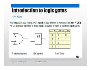
- 93. Introduction to logic gates OR Gate Eng:Mohamed Loay Ali Basic Electronics 93
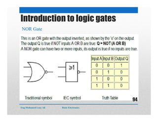
- 94. Introduction to logic gates NOR Gate Eng:Mohamed Loay Ali Basic Electronics 94