Ic technology- Crystal structure and Crystal growth
•Download as PPTX, PDF•
7 likes•4,670 views

ICs integrate thousands or millions of tiny transistors on a semiconductor wafer. They have advantages over discrete components like being smaller, faster, using less power. Moore's law observes that the number of transistors on an IC doubles every 18 months. Semiconductor substrates are wafers used to fabricate ICs. Crystal defects in wafers like point defects and dislocations can occur during manufacturing and affect processing.
Report
Share


Ic technology- Crystal structure and Crystal growth
- 1. IC TECHNOLOGY INTRODUCTION TO IC TECHNOLOGY By: Kritica Sharma Assistant Professor (ECE)
- 2. CONTENTS 2 Understanding IC Moore’s law Semiconductor Substrate Crystal defects Czochralski Growth Float Zone Wafer Preparation- Silicon Shaping, Etching and Polishing, Chemical cleaning.
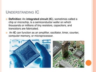
- 3. UNDERSTANDING IC Definition: An integrated circuit (IC), sometimes called a chip or microchip, is a semiconductor wafer on which thousands or millions of tiny resistors, capacitors, and transistors are fabricated. An IC can function as an amplifier, oscillator, timer, counter, computer memory, or microprocessor.
- 4. What advantages do ICs have over discrete components? Size: Sub-micron vs. millimeter/centimeter. Speed and Power: Smaller size of IC components yields higher speed and lower power consumption due to smaller parasitic resistances, capacitances and inductances. Switching between ‘0’ and ‘1’ much faster on chip than between chips. Lower power consumption => less heat => cheaper power supplies => reduced system cost. Integrated circuit manufacturing is versatile. Simply change the mask to change the design. However, designing the layout (changing the masks) is usually the most time consuming task in IC design.
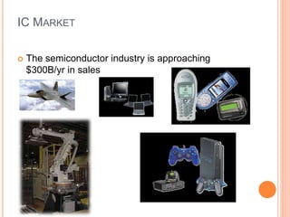
- 5. IC MARKET The semiconductor industry is approaching $300B/yr in sales
- 6. IC TECHNOLOGY INVENTION Early developments of the Integrated Circuit (IC) go back to 1949. German engineer Werner Jacobi filed a patent for an IC like semiconductor amplifying device showing five transistors on a common substrate in a 2- stage amplifier arrangement. Jacobi disclosed small cheap of hearing aids.
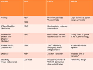
- 7. Inventor Year Circuit Remark Fleming 1904 1906 Vacuum tube diode Vacuum triode Large expensive, power- hungry, unreliable William Shockley (Bell Labs) 1945 Semiconductor replacing vacuum tube Bardeen and Brattain and Shockley (Bell labs) 1947 Point Contact transfer resistance device “BJT” Driving factor of growth of the VLSI technology Werner Jacobi (Siemens AG) 1949 1st IC containing amplifying Device 2stage amplifier No commercial use reported Shockley 1951 Junction Transistor “Practical form of transistor” Jack Kilby (Texas Instruments) July 1958 Integrated Circuits F/F With 2-T Germanium slice and gold wires Father of IC design
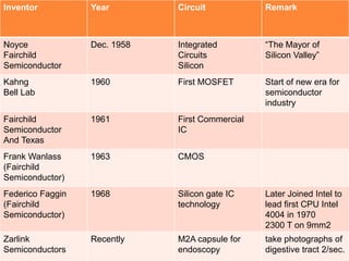
- 8. Inventor Year Circuit Remark Noyce Fairchild Semiconductor Dec. 1958 Integrated Circuits Silicon “The Mayor of Silicon Valley” Kahng Bell Lab 1960 First MOSFET Start of new era for semiconductor industry Fairchild Semiconductor And Texas 1961 First Commercial IC Frank Wanlass (Fairchild Semiconductor) 1963 CMOS Federico Faggin (Fairchild Semiconductor) 1968 Silicon gate IC technology Later Joined Intel to lead first CPU Intel 4004 in 1970 2300 T on 9mm2 Zarlink Semiconductors Recently M2A capsule for endoscopy take photographs of digestive tract 2/sec.
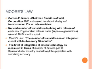
- 9. MOORE’S LAW Gordon E. Moore - Chairman Emeritus of Intel Corporation 1965 - observed trends in industry - of transistors on ICs vs. release dates: Noticed number of transistors doubling with release of each new IC generation release dates (separate generations) were all 18-24 months apart Moore’s Law: “The number of transistors on an integrated circuit will double every 18 months” The level of integration of silicon technology as measured in terms of number of devices per IC Semiconductor industry has followed this prediction with surprising accuracy.
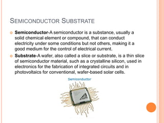
- 10. SEMICONDUCTOR SUBSTRATE Semiconductor-A semiconductor is a substance, usually a solid chemical element or compound, that can conduct electricity under some conditions but not others, making it a good medium for the control of electrical current. Substrate-A wafer, also called a slice or substrate, is a thin slice of semiconductor material, such as a crystalline silicon, used in electronics for the fabrication of integrated circuits and in photovoltaics for conventional, wafer-based solar cells.
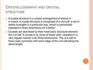
- 11. CRYSTALLOGRAPHY AND CRYSTAL STRUCTURE A crystal structure is a unique arrangement of atoms in a crystal. A crystal structure is composed of a unit cell, a set of atoms arranged in a particular way; which is periodically repeated in three dimensions on a lattice. Crystals are described by their most basic structural element: the unit cell. A crystal is an array of these cells, repeated in a very regular manner over three dimensions. The unit cell of have cubic symmetry with each edge of the unit cell being the same length.
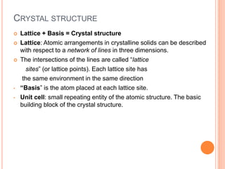
- 12. CRYSTAL STRUCTURE Lattice + Basis = Crystal structure Lattice: Atomic arrangements in crystalline solids can be described with respect to a network of lines in three dimensions. The intersections of the lines are called “lattice sites” (or lattice points). Each lattice site has the same environment in the same direction • “Basis” is the atom placed at each lattice site. • Unit cell: small repeating entity of the atomic structure. The basic building block of the crystal structure.
- 13. METALLIC CRYSTAL STRUCTURES Unit cell: small repeating entity of the atomic structure. The basic building block of the crystal structure. It defines the entire crystal structure with the atom positions within .
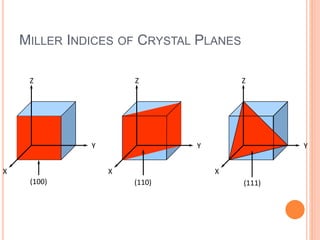
- 14. MILLER INDICES OF CRYSTAL PLANES Z X Y (100) Z X Y (110) Z X Y (111)
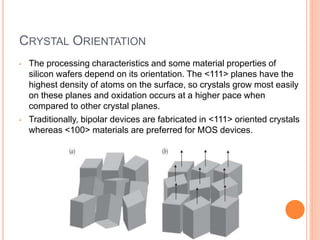
- 15. CRYSTAL ORIENTATION • The processing characteristics and some material properties of silicon wafers depend on its orientation. The <111> planes have the highest density of atoms on the surface, so crystals grow most easily on these planes and oxidation occurs at a higher pace when compared to other crystal planes. • Traditionally, bipolar devices are fabricated in <111> oriented crystals whereas <100> materials are preferred for MOS devices.
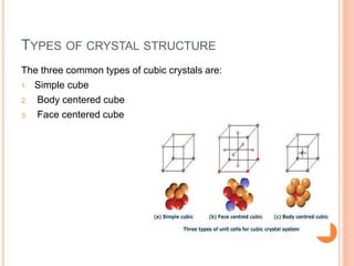
- 16. TYPES OF CRYSTAL STRUCTURE The three common types of cubic crystals are: 1. Simple cube 2. Body centered cube 3. Face centered cube
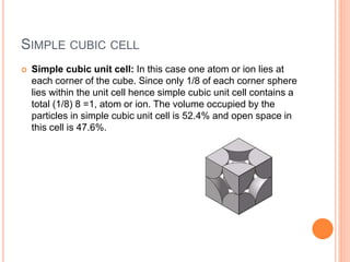
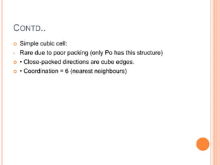
- 17. SIMPLE CUBIC CELL Simple cubic unit cell: In this case one atom or ion lies at each corner of the cube. Since only 1/8 of each corner sphere lies within the unit cell hence simple cubic unit cell contains a total (1/8) 8 =1, atom or ion. The volume occupied by the particles in simple cubic unit cell is 52.4% and open space in this cell is 47.6%.
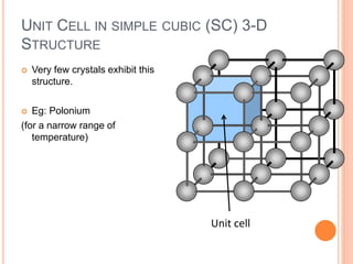
- 18. UNIT CELL IN SIMPLE CUBIC (SC) 3-D STRUCTURE Very few crystals exhibit this structure. Eg: Polonium (for a narrow range of temperature) Unit cell
- 19. CONTD.. Simple cubic cell: • Rare due to poor packing (only Po has this structure) • Close-packed directions are cube edges. • Coordination = 6 (nearest neighbours)
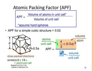
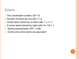
- 21. BODY CENTERED CUBIC CELL Body centred cubic unit cell: In this case one atom or ion lies at each comer of the cube and one atom (or ion) lies at the centre of the cube (unshared atom or ion). Thus the contribution of the 8 corners is (1 / 8 ) X 8 = 1, while that of the body centred (unshared atom) is 1 in the unit cell. The hard spheres touch one another along cube diagonal ⇒ the cube edge length, a= 4R/√3.
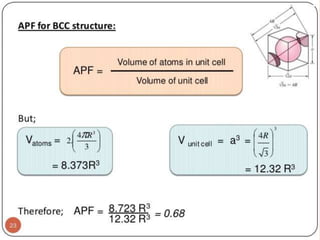
- 22. CONTD.. The coordination number, CN = 8. Number of atoms per unit cell, n = 2. Center atom shared by no other cells: 1 x 1 = 1. 8 corner atoms shared by eight cells: 8 x 1/8 = 1. Atomic packing factor, APF = 0.68. Corner and center atoms are equivalent
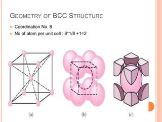
- 23. GEOMETRY OF BCC STRUCTURE Coordination No. 8 No of atom per unit cell : 8*1/8 +1=2
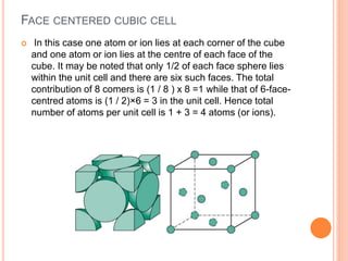
- 25. FACE CENTERED CUBIC CELL In this case one atom or ion lies at each corner of the cube and one atom or ion lies at the centre of each face of the cube. It may be noted that only 1/2 of each face sphere lies within the unit cell and there are six such faces. The total contribution of 8 comers is (1 / 8 ) x 8 =1 while that of 6-face- centred atoms is (1 / 2)×6 = 3 in the unit cell. Hence total number of atoms per unit cell is 1 + 3 = 4 atoms (or ions).
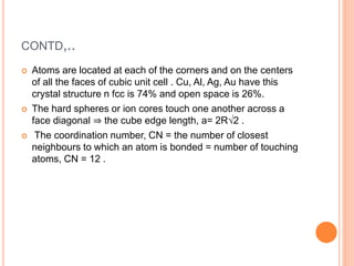
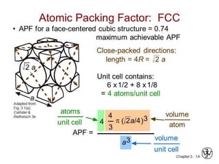
- 26. CONTD,.. Atoms are located at each of the corners and on the centers of all the faces of cubic unit cell . Cu, Al, Ag, Au have this crystal structure n fcc is 74% and open space is 26%. The hard spheres or ion cores touch one another across a face diagonal ⇒ the cube edge length, a= 2R√2 . The coordination number, CN = the number of closest neighbours to which an atom is bonded = number of touching atoms, CN = 12 .
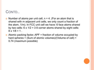
- 27. CONTD.. Number of atoms per unit cell, n = 4. (For an atom that is shared with m adjacent unit cells, we only count a fraction of the atom, 1/m). In FCC unit cell we have: 6 face atoms shared by two cells: 6 x 1/2 = 3 8 corner atoms shared by eight cells: 8 x 1/8 = 1 . Atomic packing factor, APF = fraction of volume occupied by hard spheres = (Sum of atomic volumes)/(Volume of cell) = 0.74 (maximum possible)
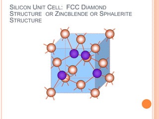
- 28. SILICON UNIT CELL: FCC DIAMOND STRUCTURE OR ZINCBLENDE OR SPHALERITE STRUCTURE
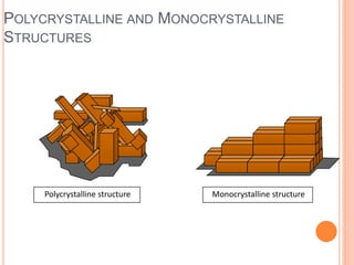
- 30. POLYCRYSTALLINE AND MONOCRYSTALLINE STRUCTURES Polycrystalline structure Monocrystalline structure
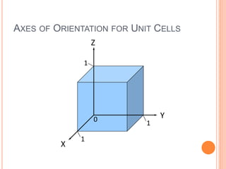
- 31. AXES OF ORIENTATION FOR UNIT CELLS Z X Y 1 1 1 0
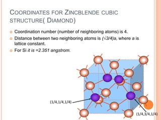
- 32. COORDINATES FOR ZINCBLENDE CUBIC STRUCTURE( DIAMOND) Coordination number (number of neighboring atoms) is 4. Distance between two neighboring atoms is (√3/4)a, where a is lattice constant. For Si it is =2.351 angstrom. (1/4,1/4,1/4) (1/4,3/4,1/4)
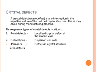
- 33. CRYSTAL DEFECTS A crystal defect (microdefect) is any interruption in the repetitive nature of the unit cell crystal structure. These may occur during manufacturing process. Three general types of crystal defects in silicon: 1. Point defects - Localized crystal defect at the atomic level 2. Dislocations - Displaced unit cells 3. Planar or - Defects in crystal structure area defects
- 34. CRYSTAL DEFECTS A perfect crystal is an idealization; there is no such thing in nature. Atom arrangements in real materials do not follow perfect crystalline patterns. Nonetheless, most of the materials that are useful in engineering are crystalline to a very good approximation. Crystalline solids exhibit a periodic crystal structure. The positions of atoms or molecules occur on repeating fixed distances, determined by the unit cell parameters. However, the arrangement of atoms or molecules in most crystalline materials is not perfect. The regular patterns are interrupted by crystallographic defects
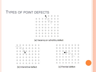
- 35. POINT DEFECTS
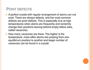
- 36. The three basic classes of defects in crystals: • Point defects - atoms missing or in irregular places in the lattice (lattice vacancies, substitutional and interstitial impurities, self- interstitials). • Linear defects - groups of atoms in irregular positions (e.g. screw and edge dislocations). • Planar defects – the interfaces between homogeneous regions of the material (grain boundaries, stacking faults, external surfaces).
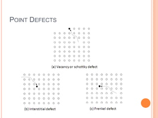
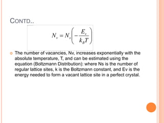
- 37. POINT DEFECTS A perfect crystal with regular arrangement of atoms can not exist. There are always defects, and the most common defects are point defects. This is especially true at high temperatures when atoms are frequently and randomly change their positions leaving behind empty lattice sites, called vacancies. How many vacancies are there: The higher is the temperature, more often atoms are jumping from one equilibrium position to another and larger number of vacancies can be found in a crystal.
- 38. CONTD.. The number of vacancies, Nv, increases exponentially with the absolute temperature, T, and can be estimated using the equation (Boltzmann Distribution): where Ns is the number of regular lattice sites, k is the Boltzmann constant, and Ev is the energy needed to form a vacant lattice site in a perfect crystal. Tk E NN B v sv
- 39. TYPES OF POINT DEFECTS
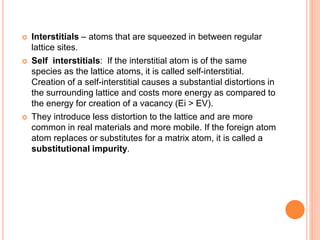
- 40. Interstitials – atoms that are squeezed in between regular lattice sites. Self interstitials: If the interstitial atom is of the same species as the lattice atoms, it is called self-interstitial. Creation of a self-interstitial causes a substantial distortions in the surrounding lattice and costs more energy as compared to the energy for creation of a vacancy (Ei > EV). They introduce less distortion to the lattice and are more common in real materials and more mobile. If the foreign atom atom replaces or substitutes for a matrix atom, it is called a substitutional impurity.
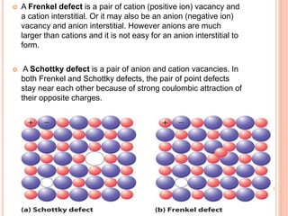
- 41. A Frenkel defect is a pair of cation (positive ion) vacancy and a cation interstitial. Or it may also be an anion (negative ion) vacancy and anion interstitial. However anions are much larger than cations and it is not easy for an anion interstitial to form. A Schottky defect is a pair of anion and cation vacancies. In both Frenkel and Schottky defects, the pair of point defects stay near each other because of strong coulombic attraction of their opposite charges.
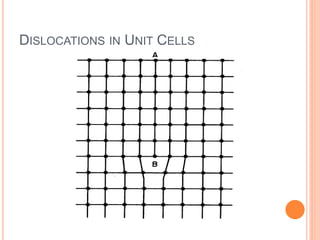
- 42. LINEAR DEFECTS- DISLOCATIONS Dislocations are another type of defect in crystals. Dislocations are areas were the atoms are out of position in the crystal structure. Dislocations are generated and move when a stress is applied. The motion of dislocations allows slip – plastic deformation to occur.
- 43. DISLOCATIONS IN UNIT CELLS
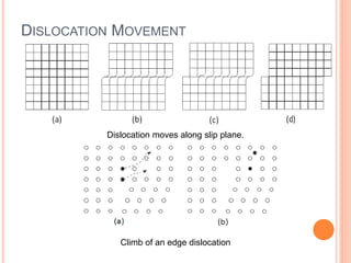
- 44. DISLOCATION MOVEMENT Dislocation moves along slip plane. Climb of an edge dislocation
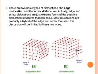
- 45. There are two basic types of dislocations, the edge dislocation and the screw dislocation. Actually, edge and screw dislocations are just extreme forms of the possible dislocation structures that can occur. Most dislocations are probably a hybrid of the edge and screw forms but this discussion will be limited to these two types.
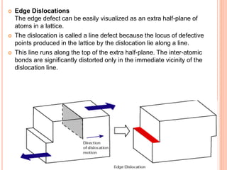
- 46. Edge Dislocations The edge defect can be easily visualized as an extra half-plane of atoms in a lattice. The dislocation is called a line defect because the locus of defective points produced in the lattice by the dislocation lie along a line. This line runs along the top of the extra half-plane. The inter-atomic bonds are significantly distorted only in the immediate vicinity of the dislocation line.
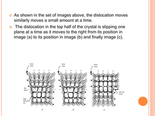
- 47. As shown in the set of images above, the dislocation moves similarly moves a small amount at a time. The dislocation in the top half of the crystal is slipping one plane at a time as it moves to the right from its position in image (a) to its position in image (b) and finally image (c).
- 48. CONTD.. In the process of slipping one plane at a time the dislocation propagates across the crystal. However, only a small fraction of the bonds are broken at any given time. Movement in this manner requires a much smaller force than breaking all the bonds across the middle plane simultaneously.
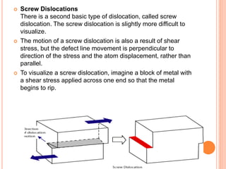
- 49. Screw Dislocations There is a second basic type of dislocation, called screw dislocation. The screw dislocation is slightly more difficult to visualize. The motion of a screw dislocation is also a result of shear stress, but the defect line movement is perpendicular to direction of the stress and the atom displacement, rather than parallel. To visualize a screw dislocation, imagine a block of metal with a shear stress applied across one end so that the metal begins to rip.
- 50. PLANAR DEFECT Stacking Faults and Twin Boundaries A disruption of the long-range stacking sequence can produce two other common types of crystal defects: 1) a stacking fault 2) a twin region.
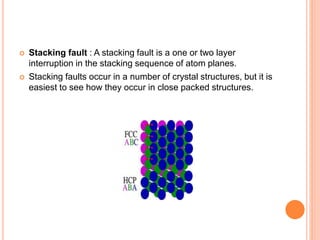
- 51. Stacking fault : A stacking fault is a one or two layer interruption in the stacking sequence of atom planes. Stacking faults occur in a number of crystal structures, but it is easiest to see how they occur in close packed structures.
- 52. Twin boundaries fault: If a stacking fault does not corrects itself immediately but continues over some number of atomic spacings. It will produce a second stacking fault that is the twin of the first one. Twin Boundaries fault
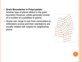
- 53. Grain Boundaries in Polycrystals: Another type of planer defect is the grain boundary However, solids generally consist of a number of crystallites or grains. Grains can range in size from nanometers to millimeters across and their orientations are usually rotated with respect to neighboring grains.
- 54. CONTD.. Where one grain stops and another begins is know as a grain boundary. .Grain boundaries limit the lengths and motions of dislocations. Therefore, having smaller grains (more grain boundary surface area) strengthens a material. The size of the grains can be controlled by the cooling rate when the material cast or heat treated.
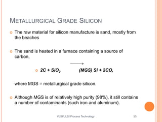
- 55. METALLURGICAL GRADE SILICON The raw material for silicon manufacture is sand, mostly from the beaches The sand is heated in a furnace containing a source of carbon, 2C + SiO2 (MGS) Si + 2CO, where MGS = metallurgical grade silicon. Although MGS is of relatively high purity (98%), it still contains a number of contaminants (such iron and aluminum). 55VLSI/ULSI Process Technology
- 56. Raw Material and Purification(EGS) -First, the MGS is reacted with HCl to form SiHCl3, (trichlorosilane) which is in liquid form at room temperature, Si (s) + 3HCl (g) SiHCl3 (g) + H2 (g) + heat -Fractional distillation results in impurity segregation, and extremely pure SiHCl3 is obtained. -To convert the SiHCl3 back into purified Si a CVD (Chemical Vapor Deposition) process is used (in a hydrogen atmosphere), 2SiHCl3 (gas)+2H2 (gas) 2Si (solid)+ 6HCl (gas), -The nucleation surface is thin poly-Si rod, with a final thickness of many inches in diameter, -All that is specified is impurity level, so fast deposition is possible . 56
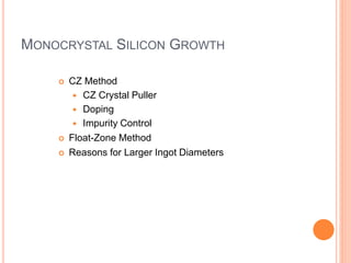
- 57. MONOCRYSTAL SILICON GROWTH CZ Method CZ Crystal Puller Doping Impurity Control Float-Zone Method Reasons for Larger Ingot Diameters
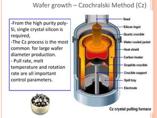
- 58. Wafer growth – Czochralski Method (Cz) -From the high purity poly- Si, single crystal silicon is required, -The Cz process is the most common for large wafer diameter production. - Pull rate, melt temperature and rotation rate are all important control parameters.
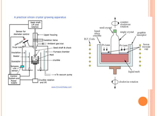
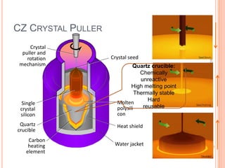
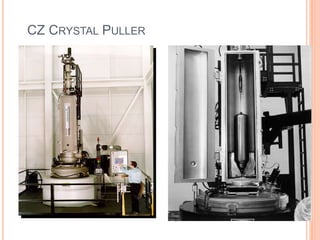
- 60. Crystal seed Molten polysili con Heat shield Water jacket Single crystal silicon Quartz crucible Carbon heating element Crystal puller and rotation mechanism CZ CRYSTAL PULLER Quartz crucible: Chemically unreactive High melting point Thermally stable Hard reusable 60
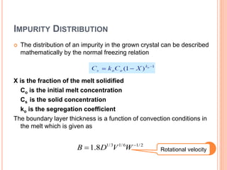
- 62. IMPURITY SEGREGATION Impurities: intentional and unintentional Equilibrium Segregation coefficient ko = Cs/Cl • Effective segregation constant, where V= growth velocity or pull rate D= diffusion coefficient of dopant in melt B= Boundary or stagnant layer thickness Cs=equilibrium concentration of impurity in solid Cl=equilibrium concentration of impurity in liquid Impurity Al As B C Cu Fe O P Sb ko 0.002 0.3 0.8 0.07 4x10⁻⁶ 8x10⁻⁶ 0.25 0.35 0.023 Segregation constants for common impurities 0 0 0(1 )exp( / ) e k k k k VB D
- 63. IMPURITY DISTRIBUTION The distribution of an impurity in the grown crystal can be described mathematically by the normal freezing relation X is the fraction of the melt solidified Co is the initial melt concentration Cs is the solid concentration ko is the segregation coefficient The boundary layer thickness is a function of convection conditions in the melt which is given as 1/3 1/6 1/ 2 1.8B D V W Rotational velocity
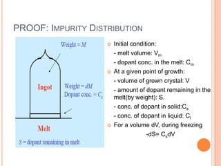
- 64. PROOF: IMPURITY DISTRIBUTION Initial condition: - melt volume: Vm - dopant conc. in the melt: Cm At a given point of growth: - volume of grown crystal: V - amount of dopant remaining in the melt(by weight): S. - conc. of dopant in solid:Cs - conc. of dopant in liquid: Cl For a volume dV, during freezing -dS= CsdV
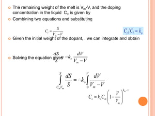
- 65. The remaining weight of the melt is Vm-V, and the doping concentration in the liquid Cl, is given by Combining two equations and substituting Given the initial weight of the dopant, , we can integrate and obtain Solving the equation gives l m S C V V o m dS dV k S V V 0m m S V o mC V dS dV k S V V 1 1 mk s o m m V C k C V
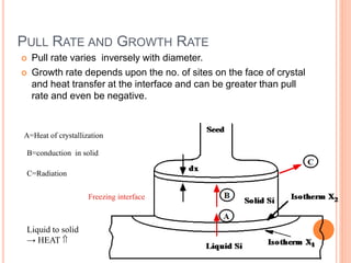
- 66. PULL RATE AND GROWTH RATE Pull rate varies inversely with diameter. Growth rate depends upon the no. of sites on the face of crystal and heat transfer at the interface and can be greater than pull rate and even be negative. A=Heat of crystallization B=conduction in solid C=Radiation Liquid to solid → HEAT Freezing interface
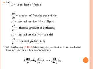
- 67. Let Then Heat balance (A B C): latent heat of crystallization + heat conducted from melt to crystal = heat conducted away. L latent heat of fusion dm dt amount of freezing per unit time kL thermal conductivity of liquid dT dx1 thermal gradient at isothermx1 kS thermal conductivity of solid dT dx2 thermal gradient at x2 L dm dt kL dT dx 1 A1 kS dT dx 2 A2
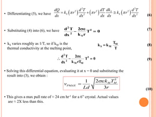
- 68. • If vP is pull rate and d is density, rate of growth of crystal is P dm v Ad dt (2) • Assuming thermal gradient in the melt be zero, eq. (1) gives: 2 S PMAX k dT v Ld dx (3) • In order to replace dT/dx2, we need to consider the heat transfer processes. • Heat radiation from the crystal (C) is given by the Stefan-Boltzmann law dQ 2rdx T4 (4) • Heat conduction up the crystal is given by Q kS r2 dT dx (5)
- 69. • Differentiating (5), we have 2 2 2 2 2 2 2 S S S dkdQ d T dT d T k r r k r dx dx dx dx dx (6) • Substituting (4) into (6), we have d2 T dx 2 2 kSr T4 0 (7) • kS varies roughly as 1/T, so if kM is the thermal conductivity at the melting point, kS kM TM T (8) d2 T dx 2 2 kM rTM T5 0 (9) • Solving this differential equation, evaluating it at x = 0 and substituting the result into (3), we obtain : 5 21 3 M M PMAX k T v Ld r (10) • This gives a max pull rate of ≈ 24 cm hr-1 for a 6” crystal. Actual values are ≈ 2X less than this.
- 70. ADVANTAGES: Growth from free surface (accommodates volume change). Crystal can be observed. Forced convection easy to impose. High throughput; large crystals can be obtained. High crystalline perfection can be achieved. Good radial homogeneity.
- 71. DRAWBACKS: Materials with high vapor pressure can not be grown. Batch process; hard to adapt for continuous growth; result: axial segregation. The crystal has to be rotated; rotation of the crucible is desirable. Process requires continuous attention (seeding, necking) and sophisticated control.
- 72. DRAWBACKS (CONTINUED): Melt is thermally upside down. Temperature gradients are high to control the crystal diameter. High thermal stresses. Shape and size of the crystal is hard to control if temperature gradients are low.
- 73. ADVANTAGES/DISADVANTAGES TO CZ METHOD Crystals grown by the CZ method are preferred for VLSI applications since they can withstand thermal stresses better than Float Zone material. The CZ method is also more cost effective, as it is capable of producing larger crystals (almost 2 meters long and with diameters of greater than 300 mm). A critical shortcoming of the CZ method is that oxygen from the silica crucible is transferred into the crystal. CZ wafers must undergo a special process to minimize the effect of oxygen on finished circuits.
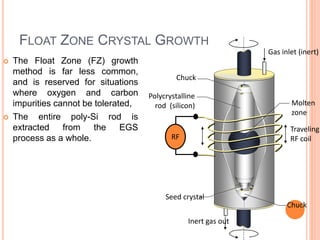
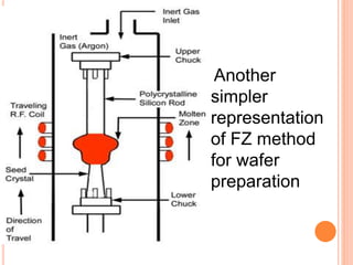
- 74. FLOAT ZONE CRYSTAL GROWTH The Float Zone (FZ) growth method is far less common, and is reserved for situations where oxygen and carbon impurities cannot be tolerated, The entire poly-Si rod is extracted from the EGS process as a whole. RF Gas inlet (inert) Molten zone Traveling RF coil Polycrystalline rod (silicon) Seed crystal Inert gas out Chuck Chuck
- 75. Another simpler representation of FZ method for wafer preparation
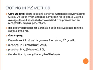
- 76. DOPING IN FZ METHOD Core Doping: refers to doping achieved with doped polycrystalline Si rod. On top of which undoped polysilicon rod is placed until the average desired concentration is reached. The process can be repeated for several generations. It is preferred process for Boron as it does not evaporate from the surface of the rod. Gas doping: Dopants are introduced in gaseous form during FZ growth. n-doping: PH3 (Phosphine), AsCl3 p-doping: B2H6 (Diborane), BCl3 Good uniformity along the length of the boule.
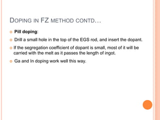
- 77. DOPING IN FZ METHOD CONTD… Pill doping: Drill a small hole in the top of the EGS rod, and insert the dopant. If the segregation coefficient of dopant is small, most of it will be carried with the melt as it passes the length of ingot. Ga and In doping work well this way.
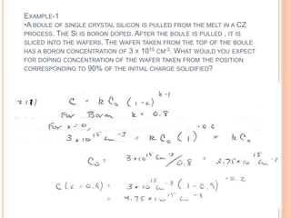
- 78. EXAMPLE-1 •A BOULE OF SINGLE CRYSTAL SILICON IS PULLED FROM THE MELT IN A CZ PROCESS. THE SI IS BORON DOPED. AFTER THE BOULE IS PULLED , IT IS SLICED INTO THE WAFERS. THE WAFER TAKEN FROM THE TOP OF THE BOULE HAS A BORON CONCENTRATION OF 3 X 10¹⁵ CM-3. WHAT WOULD YOU EXPECT FOR DOPING CONCENTRATION OF THE WAFER TAKEN FROM THE POSITION CORRESPONDING TO 90% OF THE INITIAL CHARGE SOLIDIFIED?
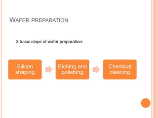
- 79. WAFER PREPARATION Silicon shaping Etching and polishing Chemical cleaning 3 basic steps of wafer preparation:
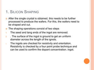
- 80. 1. SILICON SHAPING After the single crystal is obtained, this needs to be further processed to produce the wafers. For this, the wafers need to be shaped and cut. The shaping operations consist of two steps 1. The seed and tang ends of the ingot are removed. 2. . The surface of the ingot is ground to get an uniform diameter across the length of the ignots. o The ingots are checked for resistivity and orientation. Resistivity is checked by a four point probe technique and can be used to confirm the dopant concentration. ingot.
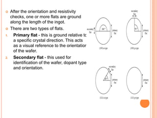
- 81. After the orientation and resistivity checks, one or more flats are ground along the length of the ingot. There are two types of flats. 1. Primary flat - this is ground relative to a specific crystal direction. This acts as a visual reference to the orientation of the wafer. 2. Secondary flat - this used for identification of the wafer, dopant type and orientation.
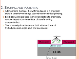
- 82. 2. ETCHING AND POLISHING After grinding the flats, the wafer is dipped in a chemical etchant to remove damage caused by mechanical grinding. Etching: Etching is used in microfabrication to chemically remove layers from the surface of a wafer during manufacturing. This is usually done in an acid bath with a mixture of hydrofluoric acid, nitric acid, and acetic acid.
- 83. Polishing: This process allows to attain the super-flat, mirrored surface with a remaining roughness on atomic scale. First a rough abrasive polish, followed by a chemical mechanical polishing (CMP) procedure. In CMP, a slurry of fine SiO2 particles suspended in aqueous NaOH solution is used. The pad is usually a polyester material. Polishing happens both due to mechanical abrasion and also reaction of the silicon with the NaOH solution.
- 84. CHEMICAL CLEANING Metal equipment must be cleaned from time to time to prevent damage and maintain efficiency of operation. Step 1 - Cleaning with alkali. Step 2 – Rinsing. Step 3 - Cleaning with acid. Step 4 – Rinsing. Step 5 - Passifying with alkali.