Nanophysics
- 1. Nanophysics Guidance by:- Mr. Goverdhan Yadu Submitted by:- Rahul Sahu M.Sc.- Physics 3rd Sem
- 2. Contents:- Nanophysics Nano Material Classification Example Synthesis Application
- 3. What is Nanophysics? Nanophysics is a physics which is applied at nanometer range. In nano range properties of materials are changed. Basically at nano range the surface properties of materials start dominating compare to bulk properties. In surface there are dangling bond which have high surface energy compared to bulk. 1 nanometer is equal to one billionth of meter, 1 nm= 1/1000000000 meters or 10-9 meters.
- 4. Nano Material Nano Materials could be defined as the materials with at least one of its dimensions in the range of nano meter. Thus the material need not be so small that it cannot be seen, it can be a large surface or a long wire whose thickness is in the scale of nano meters. Materials of which a single unit is sized (in at least one dimension) between 1 to 1000 nanometers (10−9 meter) but usually is 1 to 100 nm.
- 5. Classification Of Nano Materials Classification is based on the number of dimensions , which are not confined to the nanoscale range (<100 nm). (1). Zero-Dimensional Nano Materials- Materials wherein all the dimensions are measured within the nanoscale which means all three dimensions are in the range of 1 to 100 nm. Most common representation of zero-dimensional nano materials are nanoparticles . Ex- Quantum Dots
- 6. (2). One-Dimensional Nano Materials- In this type of nonmaterial, one of dimension that is outside of nanoscale. One dimensional nanomaterial has contain needle shaped nanomaterial. It is include Nanorods ,Nanowires etc. Ex – Carbon Nanotubes (3). Two-Dimensional Nano Materials- In this type of nanomaterial, two of the dimensions are not confined to the nanoscale. It is include Nanocoating, Nanolayers etc. Ex - Nanofilms
- 7. (4). Three-Dimensional Nano Materials- Bulk nanomaterials are materials that are not confined to the nanoscale in any dimension. These materials are thus characterized by having three arbitrarily dimensions above 100 nm. Materials possess a nanocrystalline structure or involve the presence of features at the nanoscale. In terms of nanocrystalline structure, bulk nanomaterials can be composed of a multiple arrangement of nanosize crystals most typically in different orientations. With respect to presence of features at the nanoscale, 3-D Nanomaterials can contain dispersions of nanoparticles, bundles of nanowires and nanotubes as well as multinanolayers. Ex - Graphite
- 8. Quantum dots A quantum dot is a nanoparticle made of any semiconductor material such as silicon, cadmium selenide, cadmium sulfide, or indium arsenide. Quantum dot has larger bandgap. A quantum dot gets its name because it's a tiny speck of matter so small that it's effectively concentrated into a single point (in other words, it's zero-dimensional)
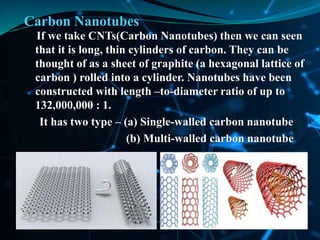
- 9. Carbon Nanotubes If we take CNTs(Carbon Nanotubes) then we can seen that it is long, thin cylinders of carbon. They can be thought of as a sheet of graphite (a hexagonal lattice of carbon ) rolled into a cylinder. Nanotubes have been constructed with length –to-diameter ratio of up to 132,000,000 : 1. It has two type – (a) Single-walled carbon nanotube (b) Multi-walled carbon nanotube
- 10. Nanofilms A thin film is a layer of material ranging from fractions of a nanometer (monolayer) to several micrometers in thickness. A familiar example is the household mirror, which typically has a thin metal coating on the back of a sheet of glass to form a reflective interface. The process of silvering was once commonly used to produce mirrors, while more recently the metal layer is deposited using techniques such as sputtering. It is also being applied to pharmaceuticals, via thin-film drug delivery. A stack of thin films is called a multilayer.
- 11. Graphite Layer structure with strong bonding within the planar layers and weak, vander-waals bonding between layers. It is good electrical conductor. Chemically stable even at high temperatures . It is a layered compound. In each layer, the carbon atoms are arranged in a hexagonal lattice with separation of 0.142 nm and the distance between planes is 0.335 nm.
- 12. Synthesis There are two approaches for synthesis of nanomaterials– (1) Top - Down approach:- This is a technique in which materials and devices are synthesized or constructed by removing existing material from larger entities. Top down approach refers to slicing or successive cutting of a bulk material to get nano sized particle. In this approach the starting material is solid state. Deposition over a large substrate is possible. Chemical purification is not required. Control over deposition parameters is difficult to achieve. Varied particle shapes or geometry.
- 13. (2) Bottom – Up approach This is a technique in which materials and devices are built up atom by atom i.e. a technique to collect, consolidate and fashion individual atoms and molecules into the structure. Atom by atom deposition leads to formation of self – assembly of atoms/molecules and clusters. These clusters come together to form self - assembled monolayer on the surface of substrate. All the bottom-up techniques, the starting material is either gaseous state or liquid state of matter. In this approach the deposition parameters can be controlled . Large scale production is difficult and chemical purification of nanoparticles is required.
- 14. Top – Down Bottom – Up Atoms Clusters
- 15. Applications Medicine Computers Electronics Textile Military
- 16. Video


