Location via proxy:   [ UP ]  
[Report a bug]   [Manage cookies]                
SlideShare a Scribd company logo
ECE614: Device
Modelling and Circuit
SimulationSimulation
Unit 2 Photolithography
By Dr. Ghanshyam Singh
Sharda University
Outline
ā€¢ Photolithography
ā€“ An introduction
ā€“ Photoresist (PR/resist)
ā€¢ PR applicationā€¢ PR application
ā€¢ Positive and Negative PR
ā€“ Soft and hard baking
ā€“ Alignment and Resist Exposure
ā€“ PR Development
Introduction
ā€¢ Photolithography literally meaning light-stone-
writing in Greek, is the process by which patterns
on a semiconductor material can be defined using
light.
ā€¢ Photolithography is an optical means for
transferring patterns onto a substrate.transferring patterns onto a substrate.
ā€¢ Patterns are first transferred to an imagable
photoresist layer.
ā€¢ Photoresist is a liquid that can be applied onto a
substrate, exposed with a desired pattern, and
developed into a selectively placed layer for
subsequent processing.
ā€¢ Photolithography is a binary pattern transfer: there
is no gray-scale, color, nor depth to the image.
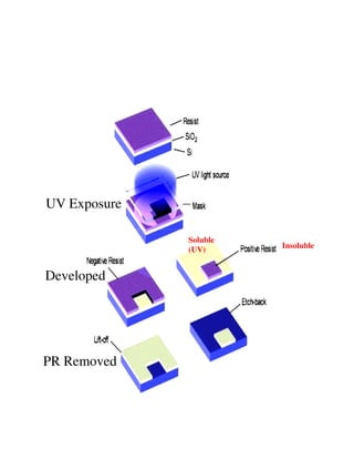
UV Exposure
Developed
PR Removed
Soluble
(UV) Insoluble
Basic of Photolithography
ā€¢ Microfabrication processes:
ā€¢ Additive (Deposition, Metallisation,
Oxidisation)
ā€¢ Subtractive (Etching)
ā€¢ Modifying (Doping, Annealing)ā€¢ Modifying (Doping, Annealing)
ā€¢ Two Primary Techniques for Additive and
subtractive processes:
ā€“ Etch-back
ā€“ Lift-off
Etch-Back
Q:What is the thickness of the substrate?
Lift-off
Making metal
contacts
Photolithography
processes
ā€¢ Surface Preparation
ā€¢ Coating
ā€¢ Soft baking
ā€¢ Alignment
ā€¢ Exposure
ā€¢ Resist Developmentā€¢ Resist Development
ā€¢ Hard Baking
ā€¢ Processing Using the Photoresist as a
Masking Film
ā€“ (Etching/Film Developing)
ā€¢ Stripping
ā€¢ Cleaning
Wafer Cleaning
ā€¢ RCA clean: use for new silicon wafers out
of the box
ā€“ 1. SC1 @70 ĀŗC for 15 min
ā€“ 2. DI water rinse for 5 min
ā€“ 3. SC2 @70 ĀŗC for 15 min
ā€“ 4. DI water rinse for 5 min
ā€“ 5. Spin and rinse dry
ā€¢ Standard degrease
ā€“ 5 min soak in Acetone > Methanol > DI water
with Ultrasonic > spin dry + N2 blow off
ā€¢ Others:
ā€“ Refer to the Cleaning section
Wafer Priming
ā€¢ To promote adhesion (PR)
ā€¢ Method:
ā€“ 15 min in 80-90ĀŗC in convention
ovenoven
Photoresist
ā€¢ It is a must for Photolithography
ā€¢ Photoresist is an organic polymer which
becomes soluble/insoluble when exposed to
ultraviolet light. It contains a light-sensitive
substance whose properties allow image
transfer onto a PCB board. Using photoresisttransfer onto a PCB board. Using photoresist
prevents etching or plating of the area it covers
(this is also known as resist).
ā€¢ Goals
ā€“ is to deposit a uniform, adherent,
defect-free and etch resistance
photoresist (PR) film on a wafer.
What is a Resist?
ā€¢ There are 4 basic ingredients in PR
ā€“ Polymers
ā€“ Designed to react with UV / laser sources / X-ray /e-
Beam
ā€“ Large and heavy molecules
ā€“ Photosensitive
ā€“ Solvents:
ā€“ As a form of liquid and allows application to waferā€“ As a form of liquid and allows application to wafer
surface by spinning
ā€“ Sensitisers
ā€“ to control the reaction (broaden or narrow)
ā€“ Additives
ā€“ to control light rays in the resist film(-PR), inhibit
dissolution of the non-exposed parts(+PR)
Positive and Negative
Resist
ā€¢ Positive PR
ā€¢ After exposure to the proper light
energy, the polymers are converted
into a more soluble state.
ā€¢ Advantages:ā€¢ Advantages:
Ā» The unexposed region do not swell
much
Ā» Higher resolution than -PR
Ā» Response to 300-400 nm spectral
range
Ā» More etch resistance, thermal
stability
Ā» Reliable
Ā» 1-3 micron thick (Typical after
baking 1 Āµm)
Positive and Negative
PR
ā€¢ Negative PR
ā€¢ The first photoresist to be used
ā€¢ After exposure to proper light
energy, the polymers are converted
into a less soluble stateinto a less soluble state
ā€¢ Limited resolution
ā€¢ Health/Environment hazard
ā€¢ Cheap
Performance factors for selection of
+PR and -PR
ā€¢ Resolution capability
ā€“ The smallest opening or line that can be
produced in a photoresist patterned layer
ā€“ Positive PR > Negative PR
ā€“ Polymer components are smaller
ā€¢ Adhesion capabilityā€¢ Adhesion capability
ā€“ A PR must have good adhesion property.
Lack of adhesion normally results in
distorted images.
ā€“ Positive PR < Negative PR
ā€“ Can use adhesion promoter (wafer priming)
Performance factors for selection of
+PR and -PR
ā€¢ Pin-holes
ā€“ Pin-holes are microscopically small voids
in the resist bulk layer which can allow the
etchants to seep through the resist layer and
etch small holes in the wafer surface.
ā€“ Use thicker PR coating. +PR has higher
aspect ratio.
ā€“ Positive PR > Negative PRā€“ Positive PR > Negative PR
ā€¢ Exposure speed
ā€“ An important selection factor for a PR is
the response time to an energy radiation.
ā€“ Faster means more productivity
ā€“ +PR: 20-60s, while -PR 3-4 times faster
ā€“ Positive PR < Negative PR
Aspect ratio is the ratio between the image opening to the resist thickness
Performance factors for selection of
+PR and -PR
ā€¢ Exposure sensitivity
ā€“ An energy required to initiate the
polymerisation (for -PR) or
photosolubilisation ( for +PR)
ā€“ Ensure all parts of resist are fully exposed
ā€“ Depend on wavelength/energy
ā€¢ Step coverageā€¢ Step coverage
ā€“ An ability of the PR to cover the side-edge
of the surface steps produced by previous
lithography process with enough thickness
for the PR to still act as an etch barrier
ā€“ the ratio of the thickness of a film over a
step edge to the thickness in a flat area.
Most metalization processes result in a
thinner metal layer over a step than in a flat
area.
ā€“ Positive PR > Negative PR
Performance factors for selection of
+PR and -PR
ā€¢ Thermal flow
ā€“ This refers to the fluidity of the PR during
heating process
ā€“ Must be able to maintain shape and
structure during baking
ā€¢ Contrastā€¢ Contrast
ā€“ The ability of a PR to distinguish between
the light and dark portion of a mask.
ā€“ The higher the contrast, the sharper the
edge profiles of developed lines
ā€“ D0 = incident dose, D100 = completion dose
(completely dissolved, +PR)
0
100
log
1
D
D
=Ī³
Contrast
Fraction of
resist remained
A B C
A: low exposure
where almost all
-PR is removed1
Depend on resist thickness, soft bake, hard bake, radiation,
development, water, surface reflectivity and etc.
D10
0
D0
Energy dose
(mJ/cm2)
1
0
0
1
0
B: Transition
C: High
exposure where
almost all -PR
remains
Performance factors for selection of
+PR and -PR
ā€¢ Etching resistance
ā€“ The ability of a resist to withstand etching
process.
Storage and Control of
PR
ā€¢ Light and heat
ā€“ Any light or heat can activate the
transformation
ā€“ Store in brown bottles
ā€“ UV-filtered room
ā€“ Temperature controlā€“ Temperature control
ā€¢ Viscosity control
ā€“ resist container must be kept capped to
prevent the evaporation of resist
solvent, which will result in high
viscosity
ā€¢ Cleanliness
ā€“ As clean as possible, filter
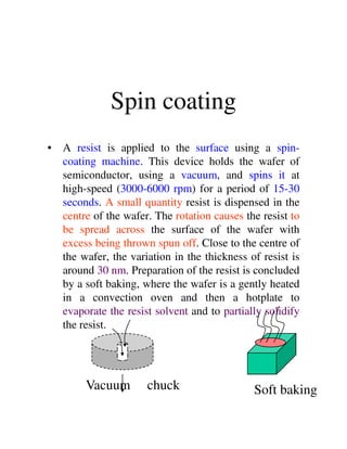
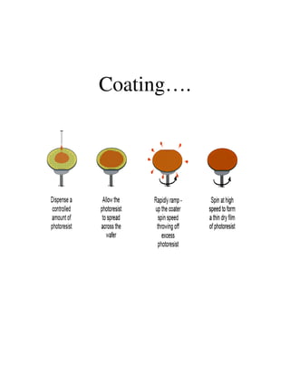
Spin coating
ā€¢ A resist is applied to the surface using a spin-
coating machine. This device holds the wafer of
semiconductor, using a vacuum, and spins it at
high-speed (3000-6000 rpm) for a period of 15-30
seconds. A small quantity resist is dispensed in the
centre of the wafer. The rotation causes the resist to
be spread across the surface of the wafer withbe spread across the surface of the wafer with
excess being thrown spun off. Close to the centre of
the wafer, the variation in the thickness of resist is
around 30 nm. Preparation of the resist is concluded
by a soft baking, where the wafer is a gently heated
in a convection oven and then a hotplate to
evaporate the resist solvent and to partially solidify
the resist.
Vacuum chuck Soft baking
Coatingā€¦.
PR spin-coating thickness
ā€¢ Resist thickness is set by
ā€¢ viscosity
ā€¢ rotational speed
ā€¢ Resist thickness is given by t=kp2/w1/2,
wherewhere
ā€¢ k=spinner constant (80-100)
ā€¢ p=resist solids content in percent
ā€¢ w=spinner rotational speed in
rpm/1000
ā€“ Typically 1-2 Āµm for Si processes
ā€“ Have to be measured
Problem? Edge
Bead
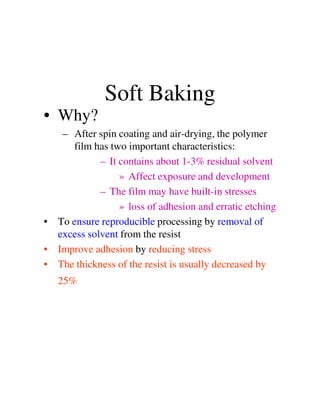
Soft Baking
ā€¢ Why?
ā€“ After spin coating and air-drying, the polymer
film has two important characteristics:
ā€“ It contains about 1-3% residual solvent
Ā» Affect exposure and development
ā€“ The film may have built-in stresses
Ā» loss of adhesion and erratic etchingĀ» loss of adhesion and erratic etching
ā€¢ To ensure reproducible processing by removal of
excess solvent from the resist
ā€¢ Improve adhesion by reducing stress
ā€¢ The thickness of the resist is usually decreased by
25%
Baking methods
Baking methods
Convention Oven: takes 30 min, good
temperature control (Tc), 400 wafer/hr,
Queuing (Q) (Solvent trapping)
Moving Belt: 5-7 min, Average Tc, 90
wafer/hr, No Qwafer/hr, No Q
Vacuum Oven: 30 min, Poor Tc, 200
wafer/hr, Queuing
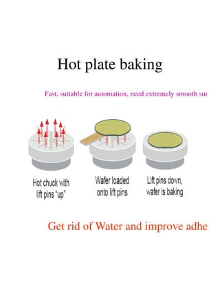
Hot Plate: 45 s, Good Tc, (No Solvent
trapping)
Microwave and IR lamps are also
available for commercial use.
Hot plate baking
Fast, suitable for automation, need extremely smooth surface
Get rid of Water and improve adhesio
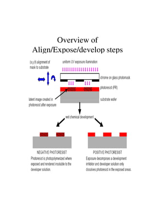
Overview of
Align/Expose/develop steps
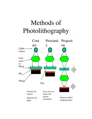
Methods of
Photolithography
Cont
act
Proximit
y
Projecti
on
Light
source
Lens
syste
m
Mask
PR
Wafer
Gap
Contact for
expose
Separate for
align
Less wear on
mask, but
poorer
resolution
Need excellent
imaging optics
Photolithography
Alignment and Exposure
ā€“ For simple contact, proximity and projection
systems, the mask is the same size and scale as
the printed wafer pattern. i.e. 1:1
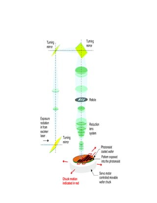
ā€“ Projection systems give the ability to change
the reproduction ratio. Going to 10:1 reduction
allows larger size patterns on the mask, whichallows larger size patterns on the mask, which
is more robust to mask defects.
ā€“ Mask size is a problem for large wafers
ā€“ Most wafers contain an array of the same
pattern, so only one cell of the array is needed
on the mask. This system is call Direct Step on
Wafer(DSW). These machines are also called
Steppers
ā€“ The mask must be perfect!
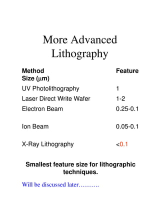
More Advanced
Lithography
Method Feature
Size (ĀµĀµĀµĀµm)
UV Photolithography 1
Laser Direct Write Wafer 1-2
Electron Beam 0.25-0.1
Ion Beam 0.05-0.1
X-Ray Lithography <0.1
Smallest feature size for lithographic
techniques.
Will be discussed laterā€¦ā€¦ā€¦.
Photomasks
ā€¢ Master patterns which are transferred to
wafers
ā€¢ Types:
ā€¢ Photographic emulsion, Fe2O3, Cr on glass
ā€¢ Cr on quartz glass (Expensive for deepā€¢ Cr on quartz glass (Expensive for deep
Uvlitho)
ā€¢ Dimensions:
ā€¢ 4ā€x4ā€x0.060ā€ for 3 inch wafers
ā€¢ 5ā€x5ā€x0.060ā€ for 4 inch wafers
ā€¢ Polarity:
ā€¢ Light field= mostly clear, drawn feature=opaque
ā€¢ Dark field=mostly opaque, drawn feature=clear
Alignment (contact type)
vacuum
mask
lev
el
lev
el
wafer
Levelling
lens
Alignin
g
lev
el
UV
Contacted+
Exposure
Resist Development
ā€¢ After exposure, the pattern is developed by the
chemical dissolution of the unpolymerised regions,
leaving the polymerised region intact on the wafer.
ā€¢ Important parameters:
ā€“ Developer strengthā€“ Developer strength
ā€“ pH
ā€“ Temperature
ā€“ Humidity
ā€¢ Problems: Resist Swelling and Distortion
ā€¢ Positive developer : KOH+H2O; Negative
developer: Organic Solvents
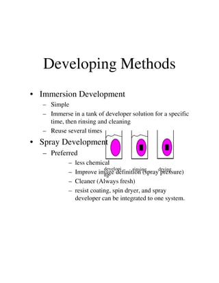
Developing Methods
ā€¢ Immersion Development
ā€“ Simple
ā€“ Immerse in a tank of developer solution for a specific
time, then rinsing and cleaning
ā€“ Reuse several times
ā€¢ Spray Developmentā€¢ Spray Development
ā€“ Preferred
ā€“ less chemical
ā€“ Improve image definition (spray pressure)
ā€“ Cleaner (Always fresh)
ā€“ resist coating, spin dryer, and spray
developer can be integrated to one system.
developi
ng
rinsing drying
Developers
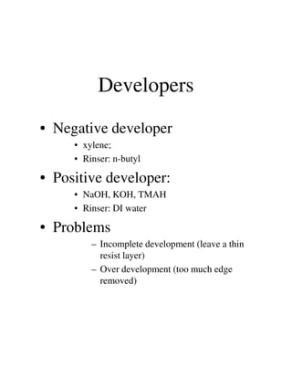
ā€¢ Negative developer
ā€¢ xylene;
ā€¢ Rinser: n-butyl
ā€¢ Positive developer:
ā€¢ NaOH, KOH, TMAHā€¢ NaOH, KOH, TMAH
ā€¢ Rinser: DI water
ā€¢ Problems
ā€“ Incomplete development (leave a thin
resist layer)
ā€“ Over development (too much edge
removed)
Development Inspection
ā€¢ The first quality check after the
photolithography process is performed
after developing and baking.
ā€¢ Checking:
ā€¢ Pattern Startā€¢ Pattern
ā€¢ Misaligned pattern
ā€¢ Surface problems
(contamination/holes/lines..)
ā€¢ Distorted pattern
Start
again!
After
developing
mask
Short,
contact
Hard Bake
ā€¢ Used to stabilise and harden the
developed photoresist.
ā€¢ Hard Bake removes any
remaining traces of the coatingremaining traces of the coating
solvent or developer
ā€¢ Introduces some stress into the
photoresist
ā€¢ Some shrinkage
ā€¢ Longer or hotter hard bake
makes resist removal much
more difficult
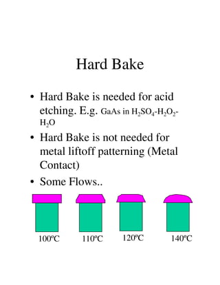
Hard Bake
ā€¢ Hard Bake is needed for acid
etching. E.g. GaAs in H2SO4-H2O2-
H2O
ā€¢ Hard Bake is not needed forā€¢ Hard Bake is not needed for
metal liftoff patterning (Metal
Contact)
ā€¢ Some Flows..
100ĀŗC 110ĀŗC 120ĀŗC 140ĀŗC
Photoresist Removal
ā€¢ Want to remove the photoresist and any of
its residues
ā€¢ Positive PR:
ā€¢ Acetone,
ā€¢ solventsā€¢ solvents
ā€¢ Negative PR:
ā€¢ CH3COC2H5(MEK),
ā€¢ CH4COC4H9 (MIBK)
Etching
ā€¢ Is to remove unwanted regions,
where are not protected by resist
ā€¢ Two main Etching Methods
ā€¢ Wet Chemical Etchingā€¢ Wet Chemical Etching
ā€“ Difficult to control
ā€“ Cheapest
ā€¢ Dry Etching
ā€“ Ion Beam
ā€“ RIE
ā€“ Plasma
More accurate, but
expensive
Final Inspection
ā€¢ Checking for
ā€¢ Dimensions
ā€¢ Misaligned pattern
ā€¢ Distorted shape
ā€¢ Surface problems
Ā» Contamination
Ā» holes
Ā» scratches
ā€¢ Electrical properties: resistivity
etc.

More Related Content

Photolithography

  • 1. ECE614: Device Modelling and Circuit SimulationSimulation Unit 2 Photolithography By Dr. Ghanshyam Singh Sharda University
  • 2. Outline ā€¢ Photolithography ā€“ An introduction ā€“ Photoresist (PR/resist) ā€¢ PR applicationā€¢ PR application ā€¢ Positive and Negative PR ā€“ Soft and hard baking ā€“ Alignment and Resist Exposure ā€“ PR Development
  • 3. Introduction ā€¢ Photolithography literally meaning light-stone- writing in Greek, is the process by which patterns on a semiconductor material can be defined using light. ā€¢ Photolithography is an optical means for transferring patterns onto a substrate.transferring patterns onto a substrate. ā€¢ Patterns are first transferred to an imagable photoresist layer. ā€¢ Photoresist is a liquid that can be applied onto a substrate, exposed with a desired pattern, and developed into a selectively placed layer for subsequent processing. ā€¢ Photolithography is a binary pattern transfer: there is no gray-scale, color, nor depth to the image.
  • 5. Basic of Photolithography ā€¢ Microfabrication processes: ā€¢ Additive (Deposition, Metallisation, Oxidisation) ā€¢ Subtractive (Etching) ā€¢ Modifying (Doping, Annealing)ā€¢ Modifying (Doping, Annealing) ā€¢ Two Primary Techniques for Additive and subtractive processes: ā€“ Etch-back ā€“ Lift-off
  • 6. Etch-Back Q:What is the thickness of the substrate?
  • 8. Photolithography processes ā€¢ Surface Preparation ā€¢ Coating ā€¢ Soft baking ā€¢ Alignment ā€¢ Exposure ā€¢ Resist Developmentā€¢ Resist Development ā€¢ Hard Baking ā€¢ Processing Using the Photoresist as a Masking Film ā€“ (Etching/Film Developing) ā€¢ Stripping ā€¢ Cleaning
  • 9. Wafer Cleaning ā€¢ RCA clean: use for new silicon wafers out of the box ā€“ 1. SC1 @70 ĀŗC for 15 min ā€“ 2. DI water rinse for 5 min ā€“ 3. SC2 @70 ĀŗC for 15 min ā€“ 4. DI water rinse for 5 min ā€“ 5. Spin and rinse dry ā€¢ Standard degrease ā€“ 5 min soak in Acetone > Methanol > DI water with Ultrasonic > spin dry + N2 blow off ā€¢ Others: ā€“ Refer to the Cleaning section
  • 10. Wafer Priming ā€¢ To promote adhesion (PR) ā€¢ Method: ā€“ 15 min in 80-90ĀŗC in convention ovenoven
  • 11. Photoresist ā€¢ It is a must for Photolithography ā€¢ Photoresist is an organic polymer which becomes soluble/insoluble when exposed to ultraviolet light. It contains a light-sensitive substance whose properties allow image transfer onto a PCB board. Using photoresisttransfer onto a PCB board. Using photoresist prevents etching or plating of the area it covers (this is also known as resist). ā€¢ Goals ā€“ is to deposit a uniform, adherent, defect-free and etch resistance photoresist (PR) film on a wafer.
  • 12. What is a Resist? ā€¢ There are 4 basic ingredients in PR ā€“ Polymers ā€“ Designed to react with UV / laser sources / X-ray /e- Beam ā€“ Large and heavy molecules ā€“ Photosensitive ā€“ Solvents: ā€“ As a form of liquid and allows application to waferā€“ As a form of liquid and allows application to wafer surface by spinning ā€“ Sensitisers ā€“ to control the reaction (broaden or narrow) ā€“ Additives ā€“ to control light rays in the resist film(-PR), inhibit dissolution of the non-exposed parts(+PR)
  • 13. Positive and Negative Resist ā€¢ Positive PR ā€¢ After exposure to the proper light energy, the polymers are converted into a more soluble state. ā€¢ Advantages:ā€¢ Advantages: Ā» The unexposed region do not swell much Ā» Higher resolution than -PR Ā» Response to 300-400 nm spectral range Ā» More etch resistance, thermal stability Ā» Reliable Ā» 1-3 micron thick (Typical after baking 1 Āµm)
  • 14. Positive and Negative PR ā€¢ Negative PR ā€¢ The first photoresist to be used ā€¢ After exposure to proper light energy, the polymers are converted into a less soluble stateinto a less soluble state ā€¢ Limited resolution ā€¢ Health/Environment hazard ā€¢ Cheap
  • 15. Performance factors for selection of +PR and -PR ā€¢ Resolution capability ā€“ The smallest opening or line that can be produced in a photoresist patterned layer ā€“ Positive PR > Negative PR ā€“ Polymer components are smaller ā€¢ Adhesion capabilityā€¢ Adhesion capability ā€“ A PR must have good adhesion property. Lack of adhesion normally results in distorted images. ā€“ Positive PR < Negative PR ā€“ Can use adhesion promoter (wafer priming)
  • 16. Performance factors for selection of +PR and -PR ā€¢ Pin-holes ā€“ Pin-holes are microscopically small voids in the resist bulk layer which can allow the etchants to seep through the resist layer and etch small holes in the wafer surface. ā€“ Use thicker PR coating. +PR has higher aspect ratio. ā€“ Positive PR > Negative PRā€“ Positive PR > Negative PR ā€¢ Exposure speed ā€“ An important selection factor for a PR is the response time to an energy radiation. ā€“ Faster means more productivity ā€“ +PR: 20-60s, while -PR 3-4 times faster ā€“ Positive PR < Negative PR Aspect ratio is the ratio between the image opening to the resist thickness
  • 17. Performance factors for selection of +PR and -PR ā€¢ Exposure sensitivity ā€“ An energy required to initiate the polymerisation (for -PR) or photosolubilisation ( for +PR) ā€“ Ensure all parts of resist are fully exposed ā€“ Depend on wavelength/energy ā€¢ Step coverageā€¢ Step coverage ā€“ An ability of the PR to cover the side-edge of the surface steps produced by previous lithography process with enough thickness for the PR to still act as an etch barrier ā€“ the ratio of the thickness of a film over a step edge to the thickness in a flat area. Most metalization processes result in a thinner metal layer over a step than in a flat area. ā€“ Positive PR > Negative PR
  • 18. Performance factors for selection of +PR and -PR ā€¢ Thermal flow ā€“ This refers to the fluidity of the PR during heating process ā€“ Must be able to maintain shape and structure during baking ā€¢ Contrastā€¢ Contrast ā€“ The ability of a PR to distinguish between the light and dark portion of a mask. ā€“ The higher the contrast, the sharper the edge profiles of developed lines ā€“ D0 = incident dose, D100 = completion dose (completely dissolved, +PR) 0 100 log 1 D D =Ī³
  • 19. Contrast Fraction of resist remained A B C A: low exposure where almost all -PR is removed1 Depend on resist thickness, soft bake, hard bake, radiation, development, water, surface reflectivity and etc. D10 0 D0 Energy dose (mJ/cm2) 1 0 0 1 0 B: Transition C: High exposure where almost all -PR remains
  • 20. Performance factors for selection of +PR and -PR ā€¢ Etching resistance ā€“ The ability of a resist to withstand etching process.
  • 21. Storage and Control of PR ā€¢ Light and heat ā€“ Any light or heat can activate the transformation ā€“ Store in brown bottles ā€“ UV-filtered room ā€“ Temperature controlā€“ Temperature control ā€¢ Viscosity control ā€“ resist container must be kept capped to prevent the evaporation of resist solvent, which will result in high viscosity ā€¢ Cleanliness ā€“ As clean as possible, filter
  • 22. Spin coating ā€¢ A resist is applied to the surface using a spin- coating machine. This device holds the wafer of semiconductor, using a vacuum, and spins it at high-speed (3000-6000 rpm) for a period of 15-30 seconds. A small quantity resist is dispensed in the centre of the wafer. The rotation causes the resist to be spread across the surface of the wafer withbe spread across the surface of the wafer with excess being thrown spun off. Close to the centre of the wafer, the variation in the thickness of resist is around 30 nm. Preparation of the resist is concluded by a soft baking, where the wafer is a gently heated in a convection oven and then a hotplate to evaporate the resist solvent and to partially solidify the resist. Vacuum chuck Soft baking
  • 24. PR spin-coating thickness ā€¢ Resist thickness is set by ā€¢ viscosity ā€¢ rotational speed ā€¢ Resist thickness is given by t=kp2/w1/2, wherewhere ā€¢ k=spinner constant (80-100) ā€¢ p=resist solids content in percent ā€¢ w=spinner rotational speed in rpm/1000 ā€“ Typically 1-2 Āµm for Si processes ā€“ Have to be measured Problem? Edge Bead
  • 25. Soft Baking ā€¢ Why? ā€“ After spin coating and air-drying, the polymer film has two important characteristics: ā€“ It contains about 1-3% residual solvent Ā» Affect exposure and development ā€“ The film may have built-in stresses Ā» loss of adhesion and erratic etchingĀ» loss of adhesion and erratic etching ā€¢ To ensure reproducible processing by removal of excess solvent from the resist ā€¢ Improve adhesion by reducing stress ā€¢ The thickness of the resist is usually decreased by 25%
  • 27. Baking methods Convention Oven: takes 30 min, good temperature control (Tc), 400 wafer/hr, Queuing (Q) (Solvent trapping) Moving Belt: 5-7 min, Average Tc, 90 wafer/hr, No Qwafer/hr, No Q Vacuum Oven: 30 min, Poor Tc, 200 wafer/hr, Queuing Hot Plate: 45 s, Good Tc, (No Solvent trapping) Microwave and IR lamps are also available for commercial use.
  • 28. Hot plate baking Fast, suitable for automation, need extremely smooth surface Get rid of Water and improve adhesio
  • 32. Alignment and Exposure ā€“ For simple contact, proximity and projection systems, the mask is the same size and scale as the printed wafer pattern. i.e. 1:1 ā€“ Projection systems give the ability to change the reproduction ratio. Going to 10:1 reduction allows larger size patterns on the mask, whichallows larger size patterns on the mask, which is more robust to mask defects. ā€“ Mask size is a problem for large wafers ā€“ Most wafers contain an array of the same pattern, so only one cell of the array is needed on the mask. This system is call Direct Step on Wafer(DSW). These machines are also called Steppers ā€“ The mask must be perfect!
  • 33. More Advanced Lithography Method Feature Size (ĀµĀµĀµĀµm) UV Photolithography 1 Laser Direct Write Wafer 1-2 Electron Beam 0.25-0.1 Ion Beam 0.05-0.1 X-Ray Lithography <0.1 Smallest feature size for lithographic techniques. Will be discussed laterā€¦ā€¦ā€¦.
  • 34. Photomasks ā€¢ Master patterns which are transferred to wafers ā€¢ Types: ā€¢ Photographic emulsion, Fe2O3, Cr on glass ā€¢ Cr on quartz glass (Expensive for deepā€¢ Cr on quartz glass (Expensive for deep Uvlitho) ā€¢ Dimensions: ā€¢ 4ā€x4ā€x0.060ā€ for 3 inch wafers ā€¢ 5ā€x5ā€x0.060ā€ for 4 inch wafers ā€¢ Polarity: ā€¢ Light field= mostly clear, drawn feature=opaque ā€¢ Dark field=mostly opaque, drawn feature=clear
  • 36. Resist Development ā€¢ After exposure, the pattern is developed by the chemical dissolution of the unpolymerised regions, leaving the polymerised region intact on the wafer. ā€¢ Important parameters: ā€“ Developer strengthā€“ Developer strength ā€“ pH ā€“ Temperature ā€“ Humidity ā€¢ Problems: Resist Swelling and Distortion ā€¢ Positive developer : KOH+H2O; Negative developer: Organic Solvents
  • 37. Developing Methods ā€¢ Immersion Development ā€“ Simple ā€“ Immerse in a tank of developer solution for a specific time, then rinsing and cleaning ā€“ Reuse several times ā€¢ Spray Developmentā€¢ Spray Development ā€“ Preferred ā€“ less chemical ā€“ Improve image definition (spray pressure) ā€“ Cleaner (Always fresh) ā€“ resist coating, spin dryer, and spray developer can be integrated to one system. developi ng rinsing drying
  • 38. Developers ā€¢ Negative developer ā€¢ xylene; ā€¢ Rinser: n-butyl ā€¢ Positive developer: ā€¢ NaOH, KOH, TMAHā€¢ NaOH, KOH, TMAH ā€¢ Rinser: DI water ā€¢ Problems ā€“ Incomplete development (leave a thin resist layer) ā€“ Over development (too much edge removed)
  • 39. Development Inspection ā€¢ The first quality check after the photolithography process is performed after developing and baking. ā€¢ Checking: ā€¢ Pattern Startā€¢ Pattern ā€¢ Misaligned pattern ā€¢ Surface problems (contamination/holes/lines..) ā€¢ Distorted pattern Start again! After developing mask Short, contact
  • 40. Hard Bake ā€¢ Used to stabilise and harden the developed photoresist. ā€¢ Hard Bake removes any remaining traces of the coatingremaining traces of the coating solvent or developer ā€¢ Introduces some stress into the photoresist ā€¢ Some shrinkage ā€¢ Longer or hotter hard bake makes resist removal much more difficult
  • 41. Hard Bake ā€¢ Hard Bake is needed for acid etching. E.g. GaAs in H2SO4-H2O2- H2O ā€¢ Hard Bake is not needed forā€¢ Hard Bake is not needed for metal liftoff patterning (Metal Contact) ā€¢ Some Flows.. 100ĀŗC 110ĀŗC 120ĀŗC 140ĀŗC
  • 42. Photoresist Removal ā€¢ Want to remove the photoresist and any of its residues ā€¢ Positive PR: ā€¢ Acetone, ā€¢ solventsā€¢ solvents ā€¢ Negative PR: ā€¢ CH3COC2H5(MEK), ā€¢ CH4COC4H9 (MIBK)
  • 43. Etching ā€¢ Is to remove unwanted regions, where are not protected by resist ā€¢ Two main Etching Methods ā€¢ Wet Chemical Etchingā€¢ Wet Chemical Etching ā€“ Difficult to control ā€“ Cheapest ā€¢ Dry Etching ā€“ Ion Beam ā€“ RIE ā€“ Plasma More accurate, but expensive
  • 44. Final Inspection ā€¢ Checking for ā€¢ Dimensions ā€¢ Misaligned pattern ā€¢ Distorted shape ā€¢ Surface problems Ā» Contamination Ā» holes Ā» scratches ā€¢ Electrical properties: resistivity etc.