


SDAccel Design Contest: Vivado
- 1. Courses @ NECST Lorenzo Di Tucci <lorenzo.ditucci@polimi.it> Emanuele Del Sozzo <emanuele.delsozzo@polimi.it> Marco D. Santambrogio <marco.santambrogio@polimi.it> Xilinx Vivado 25/01/2018
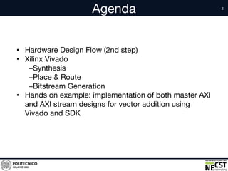
- 2. Agenda • Hardware Design Flow (2nd step) • Xilinx Vivado –Synthesis –Place & Route –Bitstream Generation • Hands on example: implementation of both master AXI and AXI stream designs for vector addition using Vivado and SDK
- 3. Reminder! Use this Google Doc to provide your data https://goo.gl/FRCG6y First, install the VPN we have provided you. (Mac: Tunnelblick - Windows/Linux: OpenVPN) To SSH to the machine: ssh <name>.<surname>@nags31.local.necst.it password: user
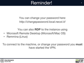
- 4. Reminder! You can change your password here: http://changepassword.local.necst.it/ You can also RDP to the instance using • Microsoft Remote Desktop (Microsoft/Mac OS) • Remmina (Linux) To connect to the machine, or change your password you must have started the VPN.
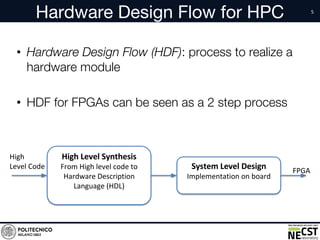
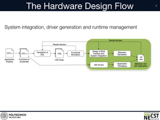
- 5. Hardware Design Flow for HPC • Hardware Design Flow (HDF): process to realize a hardware module • HDF for FPGAs can be seen as a 2 step process
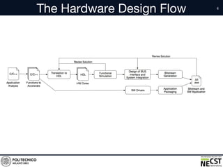
- 6. The Hardware Design Flow
- 7. The Hardware Design Flow System integration, driver generation and runtime management
- 8. The Hardware Design Flow System integration, driver generation and runtime management
- 9. The Hardware Design Flow System integration, driver generation and runtime management
- 10. Vivado Design Suite • Vivado Design Suite is a software suite for synthesis and analysis of HDL designs • Vivado enables developers to synthesize designs, perform timing analysis, examine RTL diagrams, simulate designs, and configure the target FPGA • Starting from HDL, Vivado performs several steps to eventually generate the bitstream
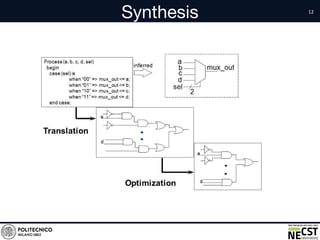
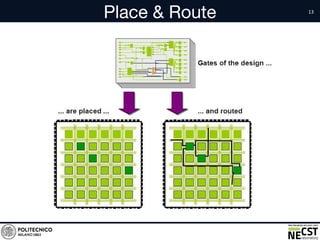
- 11. Vivado Main Steps • Synthesis: translation from HDL to gate level • Place: placing of all the logic components on the FPGA • Route: design of all the wires needed to connect the placed components • Bitstream: generation of FPGA configuration file
- 12. Synthesis
- 13. Place & Route
- 14. Bitstream
- 15. Launch Vivado Source settings64.sh file and launch vivado
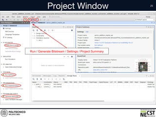
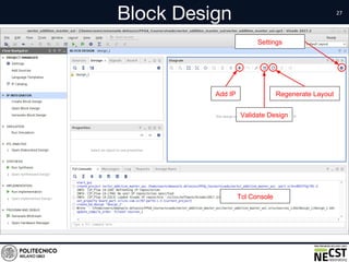
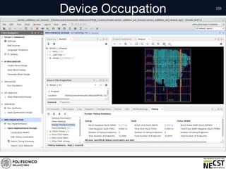
- 25. Project Window • text Run / Generate Bitstream / Settings / Project Summary
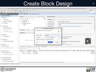
- 26. Create Block Design • text
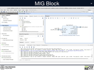
- 27. Block Design • text Add IP Validate Design Regenerate Layout Tcl Console Settings
- 28. Add IP • text
- 29. Add Memory Interface Generator • text
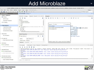
- 30. Run Block Automation • text
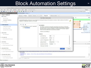
- 31. Block Automation Settings • text
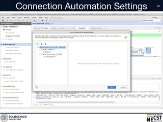
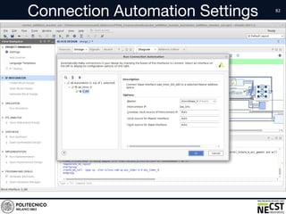
- 32. Run Connection Automation • text
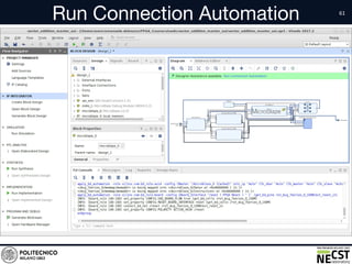
- 33. Connection Automation Settings • text
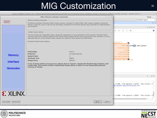
- 34. MIG Block • text
- 35. Customize MIG Block • text
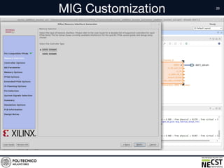
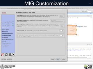
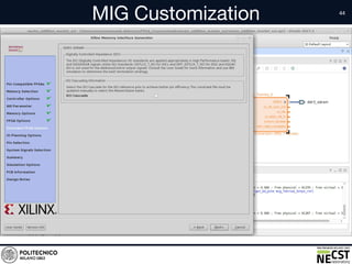
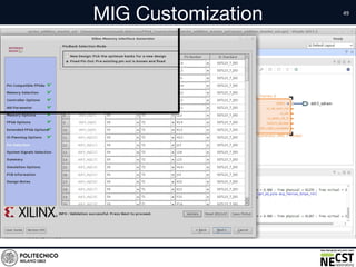
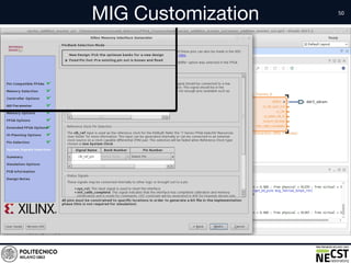
- 42. MIG Customization • text This page allows to add / customize clock signals MIG will generate two clocks: - ui_clk (200Mhz) - ui_addn_clk_0 (100Mhz)
- 55. Add IP • text
- 57. Run Block Automation • text
- 58. Block Automation Settings • text
- 59. Run Connection Automation • text
- 60. Connection Automation Settings • text
- 61. Run Connection Automation • text
- 62. Connection Automation Settings • text
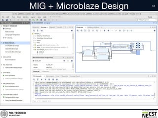
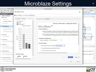
- 63. MIG + Microblaze Design • text
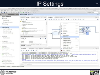
- 65. Settings • text
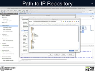
- 67. Add IP Repository • text
- 68. Path to IP Repository • text
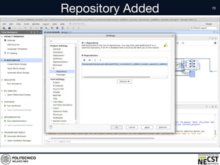
- 69. IP Found • text
- 71. Add IP • text
- 73. Connect Kernel Clock • text Connect Kernel Clock to Microblaze clock
- 74. Connection Automation Settings • text
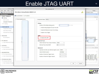
- 76. Enable JTAG UART • text
- 77. Run Connection Automation • text
- 78. Connection Automation Settings • text
- 79. Add IP • text
- 80. Add AXI Timer • text
- 81. Run Connection Automation • text
- 82. Connection Automation Settings • text
- 87. Sources • text
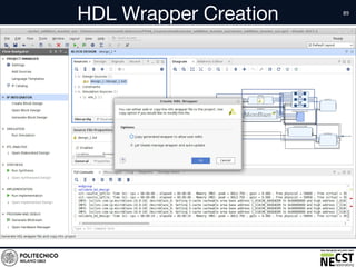
- 89. HDL Wrapper Creation • text
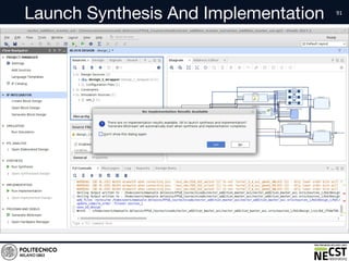
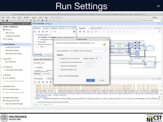
- 91. Launch Synthesis And Implementation • text
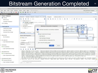
- 93. Bitstream Generation Completed • text
- 97. Export Hardware Settings • text This command will create an HDF archive containing the bitstream and drivers for SDK
- 99. Launch SDK Settings • text
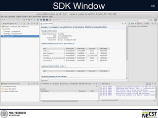
- 100. SDK Window • text
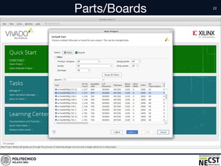
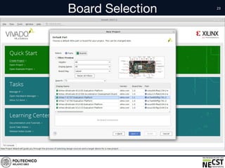
- 102. New Project • text
- 103. Templates • text
- 104. Program FPGA • text
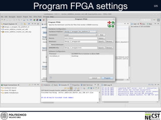
- 105. Program FPGA settings • text
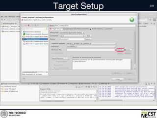
- 109. Target Setup • text
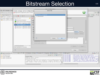
- 111. Target Setup done • text
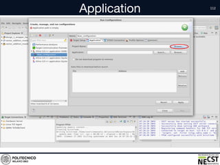
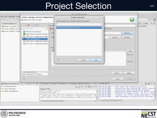
- 112. Application • text
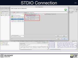
- 116. STDIO Connection done • text
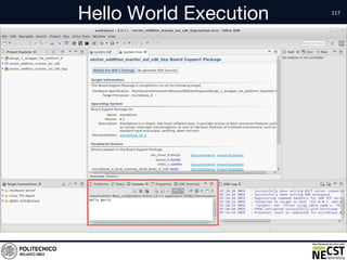
- 117. Hello World Execution • text
- 118. Lscript • text
- 119. Running Our Design • text
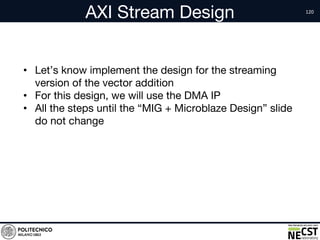
- 120. AXI Stream Design • Let’s know implement the design for the streaming version of the vector addition • For this design, we will use the DMA IP • All the steps until the “MIG + Microblaze Design” slide do not change
- 121. IP Settings • text
- 122. Settings • text
- 123. Repository • text
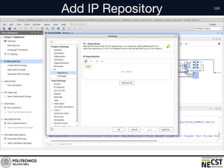
- 124. Add IP Repository • text
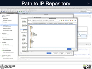
- 125. Path to IP Repository • text
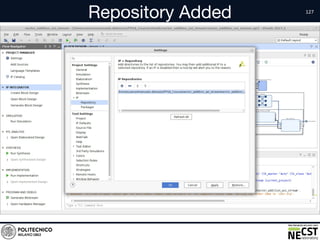
- 126. IP Found • text
- 128. Add IP • text
- 129. Add AXI DMA (0) • text
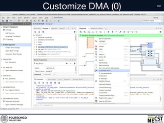
- 130. Customize DMA (0) • text
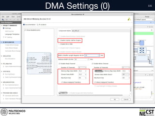
- 131. DMA Settings (0) • text
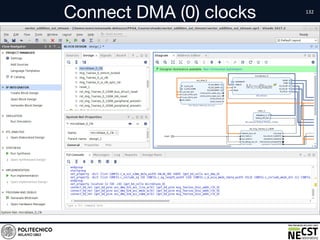
- 132. Connect DMA (0) clocks • text
- 133. Connection Automation Settings • text
- 134. Add IP • text
- 135. Add Kernel • text
- 136. Connect Kernel clock • text
- 137. Connect Kernel Reset • text
- 138. Connect port b to DMA (0) • text
- 139. Connect port a to DMA (0) • text
- 140. Add IP • text
- 141. Add AXI DMA (1) • text
- 142. Customize DMA (1) • text
- 143. DMA Settings (1) • text
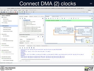
- 144. Connect DMA (1) clocks • text
- 145. Connection Automation Settings • text
- 146. Connect port c to DMA (1) • text
- 147. Add IP • text
- 148. Add AXI DMA (2) • text
- 149. Customize DMA (2) • text
- 150. DMA (2) Settings • text
- 151. Connect DMA (2) clocks • text
- 152. Connection Automation Settings • text
- 153. Connect port d to DMA (2) • text
- 154. Next steps It is now possible to repeat the steps done for the previous design: –enable JTAG UART on the MDM block –add AXI Timer IP –Run Validation –Create HDL Wrapper –Run Generate Bitstream –Export Hardware –Run SDK
- 157. SDK steps After exporting the hardware from Vivado: – Launch SDK – Create the project – Test the “helloworld” – Use the provided code to evaluate the design
- 158. Summary • Vivado toolchain allows developers to design both the IP they want to accelerate and the overall system • Vivado/Vivado HLS examples, and SDK code are available on nags31 server in /sdaccel_contest folder • Next lectures will focus on SDAccel toolchain
- 159. Feedbacks • We are working at improving this course, would you share your feedback for this lesson? https://goo.gl/tLcWQj
- 160. Thank You for the Attention! Lorenzo Di Tucci lorenzo.ditucci@polimi.it Emanuele Del Sozzo emanuele.delsozzo@polimi.it Marco D. Santambrogio marco.santambrogio@polimi.it