Location via proxy:   [ UP ]  
[Report a bug]   [Manage cookies]                
SlideShare a Scribd company logo
ARCHITECTURE
OF TMS320C5X
Deekshitha S
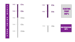
C1x1982
C2x1984
C2xx1984
C5x1989
C54x1989
C3x1988
C4x1988
C8x1994
F
I
X
E
D
P
O
I
N
T
D
S
P’
s
FLOATING
POINT
DSP’s
MULTIPROCESSOR
DSP’s
TMS320C5x Overview
● The ‘C5x generation consists of the ‘C50, ‘C51, ‘C52, ‘C53, ‘C53S,
‘C56, ‘C57 and ‘C57S DSPs, which are fabricated by CMOS
integrated-circuit technology.
● Their architectural design is based on the C25.
● The operational flexibility and speed of the ‘C5x are the result of
combining an advanced Harvard architecture.
● A CPU with application-specific hardware logic, on-chip peripherals,
on-chip memory, and a highly specialized instruction set.
● The ‘C5x is designed to execute up to 50 million instructions per
second (MIPS).
TMS320C5x Key Features
● Compatibility: Source-code compatible with C1x, C2x and
C2xx devices.
● Speed: 20-/25-/35-/50-ns single-cycle fixed-point instruction
execution time (50/40/28.6/20 MIPS)
● Power: 3.3V and 5V static CMOS technology with two power-
down modes. Power consumption control with IDLE1 and
IDLE2 instructions for power-down modes.
ARCHITECTURAL OVERVIEW
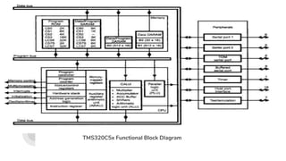
● TMS320C5x consists of buses, on-chip memory, central
processing unit (CPU), and on-chip peripherals.
● The C5x uses an advanced Harvard architecture based on
the C25 architecture and maximizes processing power with
separate buses for program memory and data memory.
● The instruction set supports data transfers between the
two memory spaces.
Architectural Overview
TMS320C5x Functional Block DIagram
Bus Structure
The C5x architecture is built around four major buses:
1. Program bus (PB)
2. Program address bus (PAB)
3. Data read bus (DB)
4. Data read address bus(DAB)
● The PAB provides addresses to program memory space for both reads and
writes.
● The PB also carrier the instruction code and immediate operands from program
memory space to the CPU.
● The DB interconnects various elements of the CPU to data memory space.
● The program and data buses can work together to transfer data from on-chip
data memory and internal or external program memory to the multiplier for
single-cycle multiply/accumulate operations.
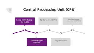
Central Processing Unit (CPU)
Memory-Mapped
Registers
Program Counter
Central Arithmetic Logic
Unit (CALU)
Parallel Logic Unit (PLU) Auxiliary Register Arithmetic
Unit(ARAU)
Auxiliary Register
Arithmetic Unit (ARAU)
Central Arithmetic Logic Unit (CALU)
The CPU uses the CALU to perform 2s-complement arithmetic.
The CALU consists of these elements:
● 16-bit x 16-bit multiplier
● 32-bit arithmetic logic unit (ALU)
● 32-bit accumulator (ACC)
● 32-bit accumulator buffer (ACCB)
● Additional shifters at the outputs of both the accumulator and
the product register (PREG)
Parallel Logic Unit (PLU)
● The CPU includes an independent PLU, which operates
separately from, but in parallel with, the ALU.
● The PLU performs Boolean operations or the bit manipulations
required of high-speed controllers.
● The PLU can set, clear, test or toggle bits in a status register,
control register, or any data memory location.
● The PLU provides a direct logic operation path to data memory
values without affecting the contents of the ACC or PREG.
Auxiliary Register Arithmetic Unit
(ARAU)
● The CPU includes an unsigned 16-bit arithmetic logic unit that
calculates indirect addresses by using inputs from the auxiliary
registers (ARs), index register (INDX) and auxiliary register compare
register (ARCR).
● The ARAU can auto index the current AR while the data memory
location is being addressed and can index either by +/-1 or by the
contents of the INDX.
● As a result, accessing data does not require the CALU for address
manipulation; therefore, the CALU is free for other operations in
parallel.
Memory-Mapped Registers
● The memory-mapped registers are used for indirect data
address pointers, temporary storage, CPU status and control
or integer arithmetic processing through the ARAU.
● Since the memory-mapped registers are a component of the
data memory space, they can be written to and read from in
the same way as any other memory location.
Program Controller
The program controller consists of these elements:
● Program Counter
● Status and Control Registers
● Hardware Stack
● Address Generation Logic
● Instruction Register
The program controller contains logic circuitry that decodes the
operational instructions, manages the CPU pipeline, stores the status
of CPU operations and decodes the conditional operations.
On-Chip Memory
On-Chip Memory
Vestibulum congue
tempus
Lorem ipsum dolor sit
amet, consectetur
adipiscing elit, sed do
eiusmod tempor.
Vestibulum congue
tempus
Lorem ipsum dolor sit
amet, consectetur
adipiscing elit, sed do
eiusmod tempor.
Vestibulum congue
tempus
Lorem ipsum dolor sit
amet, consectetur
adipiscing elit, sed do
eiusmod tempor.
Vestibulum congue tempus
Lorem ipsum dolor sit amet, consectetur adipiscing elit, sed do eiusmod tempor.
Ipsum dolor sit amet elit, sed do eiusmod tempor.
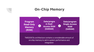
Program
Read-Only
Memory
(ROM)
Data/progra
m Dual-
Access RAM
(DARAM)
Data/program
Single-Access
RAM
(SARAM)
TMS320C5x architecture contains a considerable amount of
on-chip memory to aid in system performance and
integration
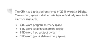
The C5x has a total address range of 224k words x 16 bits.
The memory space is divided into four individually selectable
memory segments:
● 64K-word program memory space
● 64K-word local data memory space
● 64K-word input/output ports
● 32K-word global data memory space
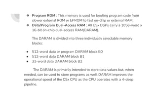
❖ Program ROM : This memory is used for booting program code from
slower external ROM or EPROM to fast on-chip or external RAM.
❖ Data/Program Dual-Access RAM : All C5x DSPs carry a 1056-word x
16-bit on-chip dual-access RAM(DARAM).
The DARAM is divided into three individually selectable memory
blocks:
● 512-word data or program DARAM block B0
● 512-word data DARAM block B1
● 32-word data DARAM block B2
The DARAM is primarily intended to store data values but, when
needed, can be used to store programs as well. DARAM improves the
operational speed of the C5x CPU as the CPU operates with a 4-deep
pipeline.
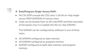
❖ Data/Program Single-Access RAM :
● All C5x DSPs except the C52 carry a 16-bit on-chip single-
access RAM (SARAM) of various sizes.
● Code can be booted from an off-chip ROM and then executed
at full speed, once it is loaded into the on-chip SARAM.
The SARAM can be configured by software in one of three
ways:
● All SARAM configured as data memory
● All SARAM configured as program memory
● SARAM configured as both data memory and program
memory
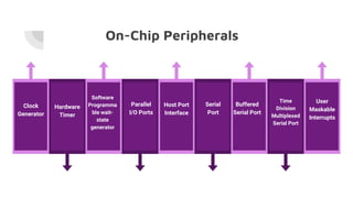
On-Chip Peripherals
On-Chip Peripherals
Hardware
Timer
Software
Programma
ble wait-
state
generator
Parallel
I/O Ports
Clock
Generator
Serial
Port
Buffered
Serial Port
Time
Division
Multiplexed
Serial Port
Host Port
Interface
User
Maskable
Interrupts
❖ Serial Port : Three different kinds of serial ports are available :
1. A general-purpose serial port
2. A Time-Division Multiplexed (TDM) serial port
3. A Buffered Serial Port (BSP)
● Each C5x contains at least one general-purpose, high-speed synchronous, full-
duplexed serial port interface that provides direct communication with serial
devices such as codes,serial analog-to-digital (A/D) converters and other serial
systems.
● The serial port is capable of operating at up to one-fourth the machine cycle rate
(CLKOUT1).
● The serial port transmitter and receiver are double-buffered and individually
controlled by maskable external interrupt signals. Data is framed either as bytes
or as words.
❖ Buffered Serial Port (BSP) :
● The BSP available on the C56 and C57 devices is a full-duplexed, double-buffered serial port
and an auto buffering unit (ABU).
● The ABU supports high-speed data transfer and reduces interrupt latencies.
❖ TDM Serial Port :
● The TDM serial port available on the C50, C51 and C53 devices is a full-duplexed serial port.
● It can be configured by software either for synchronous operations or for time-division
multiplexed operations.
● The TDM serial port is commonly used in multiprocessor applications.
❖ User-Maskable Interrupts :
1. Four external interrupt lines (INT1-INT4)
2. Five internal interrupts
3. A timer interrupt
4. Four serial port interrupts
❖ Test/Emulation : On the C50, LC50, C51, LC51, C53, LC53, C57S and LC57S an IEEE
standard 1149.1 (JTAG) interface with boundary scan capability is used for emulation
and test.
❖ Clock Generator : The clock generator consists of an internal oscillator and a phase-
locked loop (PLL) circuit. The clock generator can be driven internally by a crystal
resonator circuit or driven externally by a clock source.
❖ Hardware Timer : A 16-bit hardware timer with a 4-bit pre-scaler is
available. The timer can be stopped, restarted, reset or disabled by
specific status bits.
❖ Software-Programmable Wait-State Generators : Software-
Programmable wait-state logic is incorporated in C5x DSPs allowing
wait-state generation without any external hardware for interfacing
with slower off-chip memory and I/O devices.
❖ Parallel I/O Ports : A total of 64K ports are available, sixteen of these
ports are memory mapped in data memory space. Each of the I/O ports
can be addressed by the IN or the OUT instructions.
❖ Host Port Interface (HPI) : The HPI available on the C57S and LC57
is an 8-bit parallel I/O port that provides an interface to a host
processor.
Advantages of TMS320C5x
● Enhanced TMS320 architectural design for increased performance and
versatility.
● Modular integrated-circuit processing technology for increased
performance and low power consumption.
● Source code compatibility with C1x, C2x and C2xx DSPs for fast and
easy performance upgrades.
● Enhanced instruction set for faster algorithms and for optimized high-
level language operation.
● Reduced power consumption and increased radiation hardness
because of new static design techniques.
THANK YOU

More Related Content

TMS320C5x

  • 3. TMS320C5x Overview ● The ‘C5x generation consists of the ‘C50, ‘C51, ‘C52, ‘C53, ‘C53S, ‘C56, ‘C57 and ‘C57S DSPs, which are fabricated by CMOS integrated-circuit technology. ● Their architectural design is based on the C25. ● The operational flexibility and speed of the ‘C5x are the result of combining an advanced Harvard architecture. ● A CPU with application-specific hardware logic, on-chip peripherals, on-chip memory, and a highly specialized instruction set. ● The ‘C5x is designed to execute up to 50 million instructions per second (MIPS).
  • 4. TMS320C5x Key Features ● Compatibility: Source-code compatible with C1x, C2x and C2xx devices. ● Speed: 20-/25-/35-/50-ns single-cycle fixed-point instruction execution time (50/40/28.6/20 MIPS) ● Power: 3.3V and 5V static CMOS technology with two power- down modes. Power consumption control with IDLE1 and IDLE2 instructions for power-down modes.
  • 6. ● TMS320C5x consists of buses, on-chip memory, central processing unit (CPU), and on-chip peripherals. ● The C5x uses an advanced Harvard architecture based on the C25 architecture and maximizes processing power with separate buses for program memory and data memory. ● The instruction set supports data transfers between the two memory spaces. Architectural Overview
  • 8. Bus Structure The C5x architecture is built around four major buses: 1. Program bus (PB) 2. Program address bus (PAB) 3. Data read bus (DB) 4. Data read address bus(DAB) ● The PAB provides addresses to program memory space for both reads and writes. ● The PB also carrier the instruction code and immediate operands from program memory space to the CPU. ● The DB interconnects various elements of the CPU to data memory space. ● The program and data buses can work together to transfer data from on-chip data memory and internal or external program memory to the multiplier for single-cycle multiply/accumulate operations.
  • 9. Central Processing Unit (CPU) Memory-Mapped Registers Program Counter Central Arithmetic Logic Unit (CALU) Parallel Logic Unit (PLU) Auxiliary Register Arithmetic Unit(ARAU) Auxiliary Register Arithmetic Unit (ARAU)
  • 10. Central Arithmetic Logic Unit (CALU) The CPU uses the CALU to perform 2s-complement arithmetic. The CALU consists of these elements: ● 16-bit x 16-bit multiplier ● 32-bit arithmetic logic unit (ALU) ● 32-bit accumulator (ACC) ● 32-bit accumulator buffer (ACCB) ● Additional shifters at the outputs of both the accumulator and the product register (PREG)
  • 11. Parallel Logic Unit (PLU) ● The CPU includes an independent PLU, which operates separately from, but in parallel with, the ALU. ● The PLU performs Boolean operations or the bit manipulations required of high-speed controllers. ● The PLU can set, clear, test or toggle bits in a status register, control register, or any data memory location. ● The PLU provides a direct logic operation path to data memory values without affecting the contents of the ACC or PREG.
  • 12. Auxiliary Register Arithmetic Unit (ARAU) ● The CPU includes an unsigned 16-bit arithmetic logic unit that calculates indirect addresses by using inputs from the auxiliary registers (ARs), index register (INDX) and auxiliary register compare register (ARCR). ● The ARAU can auto index the current AR while the data memory location is being addressed and can index either by +/-1 or by the contents of the INDX. ● As a result, accessing data does not require the CALU for address manipulation; therefore, the CALU is free for other operations in parallel.
  • 13. Memory-Mapped Registers ● The memory-mapped registers are used for indirect data address pointers, temporary storage, CPU status and control or integer arithmetic processing through the ARAU. ● Since the memory-mapped registers are a component of the data memory space, they can be written to and read from in the same way as any other memory location.
  • 14. Program Controller The program controller consists of these elements: ● Program Counter ● Status and Control Registers ● Hardware Stack ● Address Generation Logic ● Instruction Register The program controller contains logic circuitry that decodes the operational instructions, manages the CPU pipeline, stores the status of CPU operations and decodes the conditional operations.
  • 16. On-Chip Memory Vestibulum congue tempus Lorem ipsum dolor sit amet, consectetur adipiscing elit, sed do eiusmod tempor. Vestibulum congue tempus Lorem ipsum dolor sit amet, consectetur adipiscing elit, sed do eiusmod tempor. Vestibulum congue tempus Lorem ipsum dolor sit amet, consectetur adipiscing elit, sed do eiusmod tempor. Vestibulum congue tempus Lorem ipsum dolor sit amet, consectetur adipiscing elit, sed do eiusmod tempor. Ipsum dolor sit amet elit, sed do eiusmod tempor. Program Read-Only Memory (ROM) Data/progra m Dual- Access RAM (DARAM) Data/program Single-Access RAM (SARAM) TMS320C5x architecture contains a considerable amount of on-chip memory to aid in system performance and integration
  • 17. The C5x has a total address range of 224k words x 16 bits. The memory space is divided into four individually selectable memory segments: ● 64K-word program memory space ● 64K-word local data memory space ● 64K-word input/output ports ● 32K-word global data memory space
  • 18. ❖ Program ROM : This memory is used for booting program code from slower external ROM or EPROM to fast on-chip or external RAM. ❖ Data/Program Dual-Access RAM : All C5x DSPs carry a 1056-word x 16-bit on-chip dual-access RAM(DARAM). The DARAM is divided into three individually selectable memory blocks: ● 512-word data or program DARAM block B0 ● 512-word data DARAM block B1 ● 32-word data DARAM block B2 The DARAM is primarily intended to store data values but, when needed, can be used to store programs as well. DARAM improves the operational speed of the C5x CPU as the CPU operates with a 4-deep pipeline.
  • 19. ❖ Data/Program Single-Access RAM : ● All C5x DSPs except the C52 carry a 16-bit on-chip single- access RAM (SARAM) of various sizes. ● Code can be booted from an off-chip ROM and then executed at full speed, once it is loaded into the on-chip SARAM. The SARAM can be configured by software in one of three ways: ● All SARAM configured as data memory ● All SARAM configured as program memory ● SARAM configured as both data memory and program memory
  • 21. On-Chip Peripherals Hardware Timer Software Programma ble wait- state generator Parallel I/O Ports Clock Generator Serial Port Buffered Serial Port Time Division Multiplexed Serial Port Host Port Interface User Maskable Interrupts
  • 22. ❖ Serial Port : Three different kinds of serial ports are available : 1. A general-purpose serial port 2. A Time-Division Multiplexed (TDM) serial port 3. A Buffered Serial Port (BSP) ● Each C5x contains at least one general-purpose, high-speed synchronous, full- duplexed serial port interface that provides direct communication with serial devices such as codes,serial analog-to-digital (A/D) converters and other serial systems. ● The serial port is capable of operating at up to one-fourth the machine cycle rate (CLKOUT1). ● The serial port transmitter and receiver are double-buffered and individually controlled by maskable external interrupt signals. Data is framed either as bytes or as words.
  • 23. ❖ Buffered Serial Port (BSP) : ● The BSP available on the C56 and C57 devices is a full-duplexed, double-buffered serial port and an auto buffering unit (ABU). ● The ABU supports high-speed data transfer and reduces interrupt latencies. ❖ TDM Serial Port : ● The TDM serial port available on the C50, C51 and C53 devices is a full-duplexed serial port. ● It can be configured by software either for synchronous operations or for time-division multiplexed operations. ● The TDM serial port is commonly used in multiprocessor applications.
  • 24. ❖ User-Maskable Interrupts : 1. Four external interrupt lines (INT1-INT4) 2. Five internal interrupts 3. A timer interrupt 4. Four serial port interrupts ❖ Test/Emulation : On the C50, LC50, C51, LC51, C53, LC53, C57S and LC57S an IEEE standard 1149.1 (JTAG) interface with boundary scan capability is used for emulation and test. ❖ Clock Generator : The clock generator consists of an internal oscillator and a phase- locked loop (PLL) circuit. The clock generator can be driven internally by a crystal resonator circuit or driven externally by a clock source.
  • 25. ❖ Hardware Timer : A 16-bit hardware timer with a 4-bit pre-scaler is available. The timer can be stopped, restarted, reset or disabled by specific status bits. ❖ Software-Programmable Wait-State Generators : Software- Programmable wait-state logic is incorporated in C5x DSPs allowing wait-state generation without any external hardware for interfacing with slower off-chip memory and I/O devices. ❖ Parallel I/O Ports : A total of 64K ports are available, sixteen of these ports are memory mapped in data memory space. Each of the I/O ports can be addressed by the IN or the OUT instructions. ❖ Host Port Interface (HPI) : The HPI available on the C57S and LC57 is an 8-bit parallel I/O port that provides an interface to a host processor.
  • 26. Advantages of TMS320C5x ● Enhanced TMS320 architectural design for increased performance and versatility. ● Modular integrated-circuit processing technology for increased performance and low power consumption. ● Source code compatibility with C1x, C2x and C2xx DSPs for fast and easy performance upgrades. ● Enhanced instruction set for faster algorithms and for optimized high- level language operation. ● Reduced power consumption and increased radiation hardness because of new static design techniques.