4764
IEEE SENSORS JOURNAL, VOL. 13, NO. 12, DECEMBER 2013
Organic Bendable and Stretchable Field Effect
Devices for Sensing Applications
Alberto Loi, Laura Basiricò, Piero Cosseddu, Stefano Lai, Massimo Barbaro, Annalisa Bonfiglio, Perla
Maiolino, Emanuele Baglini, Simone Denei, Fulvio Mastrogiovanni, and Giorgio Cannata
Abstract— In this paper we propose a detailed investigation
on the electrical response to mechanical deformations of organic
field effect transistors assembled on flexible plastic substrates.
We demonstrate that through applying a surface deformation
by an external mechanical stimulus we induce morphological
and structural changes in the organic semiconductor giving
rise to a marked, reproducible and reversible variation of the
device output current. We show how the intrinsic properties of
the employed active layers play a crucial role in determining
the final sensitivity to the mechanical deformation. Finally we
also demonstrate that the fabricated flexible system can be
successfully employed for different applications that go from the
detection of bio-mechanical parameters (e.g., joint motion, breath
rate, etc.) in the wearable electronics field to tactile transduction
for the realization of artificial robot skin
Index Terms— OFETs, strain sensors, inkjet printing, robot
skin, bio-parameters monitoring.
I. I NTRODUCTION
O
RGANIC semiconductor-based electronics has achieved
a wide consideration in the past decades, as this
new class of materials has definitely opened the way
for the fabrication of electronic devices over large areas
with cost-efficient technologies and remarkable electrical
properties [1]–[5].
One of the main advantages of employing conjugated
polymers is the fact that, thanks to their mechanical properties, it is possible to fabricate highly flexible electronic systems using these materials. However, as recently highlighted
Manuscript received December 13, 2012; revised June 14, 2013; accepted
July 2, 2013. Date of publication July 11, 2013; date of current version
October 9, 2013. This work was supported by the European Commission’s
Seventh Framework Programme project ROBOSKIN under Grant 231500.
The work of A. Loi and S. Lai was supported in part by Regione Autonoma
della Sardegna under the POR Sardegna FSE. This is an expanded paper from
the IEEE SENSORS 2012 Conference. The associate editor coordinating the
review of this paper and approving it for publication was Dr. Alexander Fish.
A. Loi, P. Cosseddu, S. Lai, M. Barbaro, and A. Bonfiglio are
with the Dipartimento di Ingegneria Elettrica ed Elettronica, University
of Cagliari, Cagliari I-09123, Italy (e-mail: alberto.loi@diee.unica.it;
piero.cosseddu@diee.unica.it;
stefano.lai@diee.unica.it;
barbaro@diee.
unica.it; annalisa@diee.unica.it).
L. Basiricò was with the Dipartimento di Ingegneria Elettrica
ed Elettronica, University of Cagliari, Cagliari I-09123, Italy. She
is now with the Istituto per lo Studio dei Materiali Nanostrutturati, Consiglio Nazionale delle Ricerche, Bologna I-40129, Italy
(e-mail: l.basirico@bo.ismn.cnr.it).
P. Maiolino, E. Baglini, S. Denei, F. Mastrogiovanni, and G. Cannata are
with the Dipartimento di Informatica, Bioingegneria, Robotica ed Ingegneria dei Sistemi, University of Genova, Genova I-16145, Italy (e-mail:
perla.maiolino@unige.it; emanuele.baglini@unige.it; simone.denei@unige.it;
fulvio.mastrogiovanni@unige.it; giorgio.cannata@unige.it).
Color versions of one or more of the figures in this paper are available
online at http://ieeexplore.ieee.org.
Digital Object Identifier 10.1109/JSEN.2013.2273173
by several research groups [6]–[13], electronic transport in
organic semiconductors is affected by mechanical deformations. The surface strain, induced on the semiconducting
layer by mechanical stress, typically leads to variations of
its structural/morphological properties, which strongly influence the charge carrier transport in Organic Field Effect
Transistors (OFETs) [6]–[10]. For applications where this
sensitivity is undesired (typically for electronic circuitry),
several approaches have been introduced for reducing the
effect of mechanical deformation on the electrical behavior
of the fabricated devices. In some cases it is reported that
by properly modifying the device structure, i.e. by placing the
organic semiconductor film on a zero strain layer, the effect of
mechanical stress can be eliminated [11]. In another example
it is also demonstrated that the employment of alkylated
molecules could be also a valuable solution, as the alkyl
chain terminations can help in accommodating most of the
surface strain induced on the semiconductor film [12]. Very
recently, Sokolov et al. [13] reported that not only the organic
semiconductor, but also the employed dielectric film plays a
crucial role in the device response to the applied strain. In
particular, by employing different polymeric gate dielectrics,
they observed a clear correlation between the sensitivity to
strain and the surface energy of the insulating film, and have
been able to fabricate devices with a very small dependence on
mechanical deformations. On the other hand, if the electrical
response of the devices is reproducible, possibly linear, and
reversible, OFETs can be employed as mechanical deformation
sensors. In fact, there are several advantages for using OFETs
in comparison with piezoresistive sensors: i) transistors are
multiparametric devices, in which different electronic parameters, not only one as for piezoresistive sensors, can be extracted
from their electrical characterization, offering the possibility
of using a combination of variables in order to characterize
their response to the parameter to be sensed; ii) in OFETs
the electrical response can be intrinsically amplified by the
transistor itself; iii) OFETs join the sensing properties with
the switching features of a transistor, allowing the fabrication
of sensors matrices in which every single element can be
addressed without additional devices. Moreover, thanks to the
intrinsic mechanical properties of organic polymers, highly
flexible and compliant systems, which can be easily transferred
on different surfaces, can be fabricated and employed for a
wide range of applications.
For these reasons, there are several examples reported in
the literature on the employment of OFETs for mechanical sensing, and in particular for reproducing the sense of
1530-437X © 2013 IEEE
�LOI et al.: ORGANIC BENDABLE AND STRETCHABLE FIELD EFFECT DEVICES FOR SENSING APPLICATIONS
4765
another dielectric layer was deposited in order to protect the
structure from the damage caused by external agents, like
oxygen and humidity.
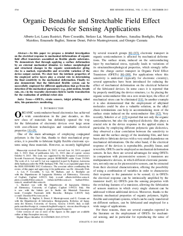
B. Plastic Substrates
Fig. 1. Schematic representation of the bottom-gate/bottom-contact OFET
structure. (a) Mylar acts at the same time as flexible substrate and as gate
dielectric. (b) All the layers are deposited on the PET substrate.
touch ([14]–[16]). For instance Someya et al. [16] fabricated
matrices of pressure sensors in which a piezoresistive rubber
was connected in series with the source electrode of each
OFET. In this way, changes in the series resistance induced
by pressure lead to a variation of the output current of the
OFET. More recently, Mansfeld et al. and Schwartz et al.
([14], [15]) reported on the fabrication of an OFET-based system for pressure sensing fabricated by a micro-structuring of
the gate dielectric, in which the capacitance changes induced
by pressure on the dielectric layer lead to a variation of the
OFET output current. The approach we have employed for
fabricating mechanical sensors is slightly different. We took
advantage of the sensitivity of the organic semiconductor films
to surface deformation, and exploited this property for the
fabrication of mechanical sensors, without adding any other
fabrication step.
In particular, in this paper we have performed a detailed
electromechanical characterization on devices realized with
two very different organic semiconductors, namely a thermally evaporated small molecule (Pentacene) and a solution
processable polymer, poly(3-hexylthiophene-2,5-diyl) (P3HT).
Interestingly enough, it was found that the intrinsic morphological properties of the two employed semiconducting films
play a crucial role in the electrical response of the devices to
mechanical deformation. We also demonstrate that, since such
a response is reproducible and reversible within a certain range
of mechanical deformation, these devices can be employed
for the fabrication of mechanical sensors on a wide range of
applications, going from tactile transduction for the realization
of artificial “robot skin” to the detection of bio-mechanical
parameters (e.g., joint motion, breath rate, etc.) in the wearable
electronics field.
II. E XPERIMENTAL
A. Fabrication Steps
All OFETs have been fabricated in a bottom-gate/bottomcontact configuration, as shown in Fig. 1. The base of the final
structure is a highly flexible substrate, where the gate electrode
was deposited by thermal evaporation or inkjet printing. The
gate dielectric was deposited from vapour phase, except for
the structure reported in Fig. 1(a), in which a very thin, freestanding, plastic film acts at the same time as flexible substrate
and as gate dielectric. Then, the source and drain electrodes
were patterned by inkjet printing or thermal evaporation. After
that, the organic semiconductor was deposited from solid
phase, by thermal evaporation, or liquid phase, by drop casting
or spin coating. Finally, in the fabrication of the robot skin,
Several substrates have been used, which differ in thickness
and thermal resistance. For the electromechanical characterization of single OFETs, a very thin, 1.5 µm thick, free-standing
poly(ethylenetherephthalate) (PET) foil (Mylar, DuPont) was
employed. In this particular case, being the film free-standing,
the gate electrode was patterned on one side of the film,
whereas source and drain and the organic semiconductor were
deposited and patterned on the opposite side (Fig. 1(a)).
For the realization of the electronic skin (structure shown
in Fig. 1(b)), three substrates were employed: 175 µm
thick PET (boPET) films (Goodfellow), 125 µm thick
poly(ethylenenaphthalate) (PEN) films (Goodfellow), and
50 µm and 13 µm thick polyimmide films (Kapton, Goodfellow). All these substrates are flexible, transparent and have
good resistance to chemical agents, but Kapton is more thermoresistant than PET and PEN. Therefore Kapton substrates
are more suitable when high-temperature annealing is required,
since no deformation occurs until temperatures as high as
500 °C. In all cases, the substrates (175 µm and 125 µm)
were cleaned by subsequent 15 min ultrasonic baths in acetone
and isopropyl alcohol, then washed with deionized water and
finally dried under nitrogen flow.
C. Electrodes
Gate, source and drain electrodes were fabricated using two
different approaches. In one case, gold electrodes have been
deposited by thermal evaporation in high-vacuum condition
and patterned using a shadow mask (for the gate) and standard
photolithography (for source and drain). For the fabrication
of matrices of OFETs, electrodes were deposited by means
of inkjet printing of a silver ink (Cabot Conductive Ink,
CCI-300), which contains surface modified ultra-fine (average
size 20 nm) silver nanoparticles dispersed in a liquid vehicle
composed of ethanol and ethylene glycol. Before filling the
printer cartridge, CCI was subjected to 15 min ultrasonic
bath and filtered with 0.2 µm nylon filter in order to avoid
agglomeration of nanoparticles.
D. Gate Dielectric
The gate dielectric layer, namely polypara-xylylene (Parylene C, purchased by Specialty Coating Systems), was
deposited from the vapor phase, using a Labcoater 2 SCS PDS
2010, according to the standard procedure described in [7]. In
order to promote the dielectric polymer adhesion on the metallic gate electrode, γ -methylacryloxypropyltrimethoxysilane
(Sylane A-147, Specialty Coating Systems) was deposited by
thermal evaporation before the deposition of Parylene. On one
hand, in order to prevent high leakage currents caused by
fractures and/or pinholes in the Parylene layer, the thickness
of the gate dielectric was set to 1.5 µm and the resulting
capacitance was 1.86 nF/cm2 . On the other hand, the layer
deposited to encapsulate the final structure was 2.5 µm thick.
�4766
Fig. 2. Picture of the interdigitated (left) and continuous (right) patterns
printed for the realization of the OFETs. The channel length is 50 µm.
E. Organic Semiconductors
Three different organic semiconductors have been employed
in this work. For the electromechanical characterization of
single OFETs, two different organic semiconductors have
been employed, namely P3HT (OS2100, purchased from Plextronics) and Pentacene (Sigma Aldrich). The first one was
dissolved in chlorobenzene (0.5 wt.%) and deposited by spin
coating at 3000 rpm for 60 s. After deposition the film was
annealed for 1 hour at 40 °C in order to remove residual
solvent. Pentacene was deposited by thermal vapor deposition
in high vacuum condition. For the fabrication of the robot
skin, a solution-processable version of Pentacene, namely
6,13-bis(triisopropylsilylethynyl)-Pentacene (TIPS-Pentacene,
Sigma Aldrich), was deposited by drop casting. The solution
was prepared at 0.5 wt.% in toluene and stirred for 1 hour at
90 °C. 1 µL drops were deposited on the transistors’ channel
while keeping the substrate on a hotplate at 90 °C, in order to
promote fast solvent evaporation and subsequently to obtain
good crystallization of the semiconductor.
F. Inkjet Printing
The main deposition technique adopted for the realization
of the robot skin was inkjet printing, performed by the
piezoelectric drop-on-demand Dimatix Materials Printer 2800
(DMP2800). We used DMC-11610 cartridges, which contain
16 nozzles with a diameter of 21.5 µm corresponding to
10 pL drops of ink. Since drop spacing (distance between
two contiguous drops), firing voltage (needed for inducing
deformation of the piezoelectric crystals) and jetting frequency
(related to the speed of the printing cartridge) strongly affect
the quality of the printed pattern, a fine preliminary tuning of
these printing parameters was mandatory.
In order to determine the resolution of the printed pattern,
single drops of CCI-300 ink were printed, showing an uniform
value of 30 µm ± 2 µm for the drop diameter on all the
substrates. When printing continuous layers, the upper value
that can be used for the drop spacing is 20 µm, because for
higher values some discontinuities occur due to the capillarity
of the ink. During printing, the substrates were kept at 60 °C
in order to promote faster solvent evaporation. After printing,
the devices were annealed at high temperature to promote the
material sintering: 1 hour at 100 °C for OFETs on Kapton, 24
hours at 60 °C for OFETs on PET.
Two main types of patterns, i.e. interdigitated and continuous patterns (Fig. 2), have been printed employing different
IEEE SENSORS JOURNAL, VOL. 13, NO. 12, DECEMBER 2013
printing setup. The interdigitated source and drain electrodes
are the core of the devices. This pattern consists of a series
of 18 lines, 50 µm thick at a distance of 50 µm, as shown in
Fig. 2 on the left hand side. We always used this configuration
in order to increase the form factor W/L, W being the channel
width and L being the channel length. We obtained W =
50 mm and L = 50 µm. On the one hand, for this type
of pattern we always printed with one nozzle using a drop
spacing of 20 µm, a firing voltage of 25 V or lower to avoid
short circuits, a jetting frequency of 2 kHz or lower to avoid
pattern discontinuities. On the other hand, printing continuous
patterns, as for example the gate electrodes, is quite easier
and does not require high precision (Fig. 2, on the right hand
side). We printed these patterns with 2–3 nozzles, using a drop
spacing of 15 µm to create continuous patterns, firing voltage
of 30 V or higher and jetting frequency of 5–10 kHz to avoid
discontinuities.
G. PDMS Substrates
Two types of polydimethylsiloxane (PDMS) were employed
for the realization of the electronic skin, both provided as twopart liquid component kit comprised of an elastomer (A) and
a curing agent (B). For the first very soft (shore 00) PDMS
(Ecoflex 00–30, purchased from Smooth-on), components A
and B were mixed together by hand in the ratio 1:1 by
volume and, subsequently, in order to avoid a detriment
of mechanical properties, air bubbles were extracted from
the obtained compound by means of a vacuum pump. The
compound was deposited over the Kapton substrate with the
printed organic array in an ad hoc mold and was polymerized
at room temperature for 4 hours. For the second, more rigid
(shore 50) PDMS (Sylgard 184, purchased from Dow Corning), components A and B were mixed by ratio 10:1 by weight,
and the compound was degassed in a vacuum pump. In this
case, the PDMS was polymerized at 100 °C for 1 hour.
H. Electrical Characterization
Electrical characterization of the OFETs was carried out
by means of a Keithley Sourcemeter 2600 in air, at room
temperature. The hole mobility µp and the threshold voltage
VT was derived from the analytical expression of the drain
current ID in saturation regime:
�
�
W
· µ p · Cins · (VG S − VT ) .
ID =
(1)
2L
III. E LECTROMECHANICAL C HARACTERIZATION OF
OFET S
In a first experiment, we have investigated the correlation between intrinsic morphological properties of the
employed organic semiconductor films and the electrical
response to mechanical deformation. In this case, devices
have been fabricated on a 1.5 µm thick, free-standing
poly(ethylenetherephtalate) (PET) foil (Mylar, DuPont), which
acts at the same time as gate dielectric and as flexible
mechanical support for the whole device, as shown in Fig. 3(a).
Such a film is glued on a circular frame so that it can be very
�LOI et al.: ORGANIC BENDABLE AND STRETCHABLE FIELD EFFECT DEVICES FOR SENSING APPLICATIONS
Fig. 3. Schematic representation of the experimental setup employed for the
electromechanical characterization (a) of single OFETs (b). AFM micrographs
of Pentacene and P3HT films (c), and electrical response to mechanical
deformation of the two different sets of samples (d).
easily patterned on both sides. To investigate the electrical
response to mechanical deformation, the apparatus shown in
Fig. 3(a) was employed. It consists of a pressurized chamber
provided with an air inlet and a circular aperture of radius
R = 1.1 cm, on the top side of which the free-standing,
patterned film can be fixed (the film is glued only on the
borders of the circular frame). When the air flows into (or
out from) the chamber, it deforms the free-standing device,
inducing an isotropic surface strain, as shown in Fig. 3(b).
The applied pressure can be monitored by a manometer, and
at the same time, taking into consideration the deformation
of the substrate, the induced surface strain can be calculated
using the methodology described by Hsu et al. [17].
Two different organic semiconductors have been employed
in this case, Pentacene and P3HT, as they are the
most common representatives of two different classes of
organic semiconductors, i.e. small molecules and polymers
respectively.
As we have already recently demonstrated [9], the electrical
response of organic semiconductors was found to be linear,
reproducible and fully reversible for a range of deformation that goes from 0% to 2% of surface strain. Moreover, as recently reported in [8], the electrical response of
small molecule-based systems (Pentacene) is much more
pronounced than the one observed in polymer-based devices
(P3HT).
In this paper we demonstrate that this difference is related
to the different morphological properties of the employed
organic semiconductors. In fact, in polycrystalline systems
like those used in this experiment, charge transport is dominated by hopping [18]. Therefore, a tensile deformation may
induce a strain of the active layer, thus leading to a possible
increase of spacing between molecules within the active layer
as stated by Yang et al. [19], and also, as suggested by
4767
Fig. 4. Example of a OFET sensor transferred on a ribbon (a); the sensor
is then sued on an elastic bend for elbow motion monitoring (b); electrical
response of the sensor to different bending angles (c) and to a cycled
measurement (d).
Sekitani et al. [6] and demonstrated by Scenev et al. [20], to
an increase in distance between adjacent crystal domains. As a
result, applying a tensile strain should lead to an increase in the
hopping barrier, which in turns causes a decrease of the OFET
mobility. As a consequence, the very different morphological
features observed in Pentacene and P3HT systems (Fig. 3(c)),
which strongly influence the transport properties of the transistors, are the main reasons for the reported differences in the
observed sensitivity to strain. Interestingly, recently it was also
found that by properly modulating the morphological features
of the deposited active layer (average grain dimensions), it
is possible to tune the sensitivity to mechanical deformation
going from insensitive devices, that could be employed for
flexible electronics applications, to highly sensitive devices
that can be used for fabricating mechanical sensors [9].
IV. A PPLICATIONS
Starting from the previous considerations, we have developed a highly flexible system for sensing mechanical deformation. In this case, devices have been fabricated on 175 µm
thick substrates, using Parylene C as gate dielectric, following
the procedures reported before in Section II.
Thanks to the noticeable flexibility of the employed structure, these devices can be easily transferred onto garments or
elastic bends for monitoring bio-mechanical parameters such
as breath rhythm or joint motion. A possible application of the
introduced system is reported in Fig. 4. In this case, as shown
in Fig. 4(a), the OFET-based sensor has been transferred on
a ribbon, and the final system has been sewed on an elastic
bend. After that, the sensor was placed in the elbow and the
electrical response of the device during the elbow motion was
monitored.
The sensor clearly detects the joint motion. The output
current decreases when the elbow is bent, accordingly to the
fact that bending the elbow induces a surface strain on the
�4768
Fig. 5.
IEEE SENSORS JOURNAL, VOL. 13, NO. 12, DECEMBER 2013
High-flexible Kapton substrates where devices are fabricated.
Fig. 7. Electrical stress induced degradation of the semiconductor performances over 380 minutes. OFETs are biased with square-wave gate voltage
(VGS from +5V to –15V) and constant VDS (–5V).
Fig. 6.
Output (a) and transfer (b) characteristics of a printed OFET.
OFET active layer. The elbow has been bent at different
bending angles, and as shown in Fig. 4(c), these different states
can be clearly detected by employing our sensing system.
Moreover, the response of the device is stable and reproducible
and did not show any significant degradation even after several
hundreds of applied bending cycles (Fig. 4(d)).
Moreover, we have also developed and tested a system
based on an array of OFET-based sensors for the realization
of a robot skin, i.e. the reproduction of the sense of touch in
robotic applications. The realization of this system has been
carried out by means of the inkjet printing technique with a
silver-based ink, as described in the Section II. Starting from
a single OFET, with W/L = 1000 and Cins = 1.86 nF/cm2 ,
we fabricated an array of 8 OFETs, with a common gate
electrode, a common source electrode and 8 independent drain
electrodes, so that each device can be addressed independently,
and with a lateral pitch of 5 mm. The most critical step of the
fabrication process is the inkjet printing of the interdigitated
source and drain electrodes, which represent the core of each
device: the fine tuning of the printing parameters, calibrated
in order to avoid short circuit and discontinuity problems,
allowed us to obtain a yield, i.e. number of working devices,
higher than 90%, and a very good reproducibility of the
electrical performances between different devices. Organic
semiconductor, TIPS-Pentacene, was deposited by means of
drop-casting.
We used different types of substrates with different thickness (as small as 13 µm), leading to the possibility of high
flexible and compliant systems (Fig. 5).
The output and the transfer characteristics of an inkjet
printed OFET are shown in Fig. 6, where a large field effect
and a very small hysteresis can be noticed. We obtained a
good mobility (0.07 ± 0.03 cm2 /(V· s), up to 0.1 cm2 /(V· s)),
slightly negative threshold voltages (−1.5 ± 1.2 V) and high
ION /IOFF (≈105).
The employment of the OFETs as strain sensors required
preliminary dynamic tests in order to investigate the real-time
response and the electrical performance over long time.
It is well known [21] that applying a DC voltage for long
time causes the degradation of the electrical performances of
the semiconductor, i.e. a reduction of the output current. For
this reason, we applied square-wave gate voltage alternatively
positive and negative, in order to reduce the bias stress effects.
We found that the best tradeoff between signal saturation and
low bias stress is obtained at 100 Hz frequency and 50% duty
cycle. Fig. 7 shows the relative variation of the output drain
current with respect to the initial on-current, measured during
a dynamic test with a square-wave gate voltage (VGS from +5
V to –15 V) and constant VDS (–5 V). The effects of the bias
stress are not very relevant: after an initial decrease, the level
of the maximum drain current does not change significantly
over more than 6 hours of biasing.
The read-out circuitry, developed ad hoc in our laboratory,
consists of 8 input channels, and analog block (I/V converter
and amplifier) and a digital block (microcontroller and analog
to digital converter, with 500 Hz sampling frequency). The
real-time Graphic User Interface evaluates the average value
of 5 acquisitions for each device and shows the relative current
variation �ID of the “pressed” state with respect to the initial
state.
The result is represented in Fig. 8, where the response of
the flexible robot skin is shown. When a certain pressure
is applied on the device structure, a variation of the output
current can be detected. In this case, an arbitrary pressure has
been exerted with a finger on a single element of the array.
It is noteworthy that, when the indenter is moved across the
array surface each device responds to the applied mechanical
deformation independently, and a very small crosstalking (both
electrical and mechanical) can be detected.
In order to gain more detailed information about the sensitivity and the reliability of the robot skin, calibration and
stress tests have been performed by means of a mechanical
indenter, shown on Fig. 9. This home-made indenter consists of a metal scaffold and a mechanical finger, controlled
in vertical position, which can move up and down with
high spatial resolution. A linear DC-servomotor (LM-1247040-02, purchased from Faulhaber) is employed to calibrate
the applied force. On the bottom of the mechanical finger,
�LOI et al.: ORGANIC BENDABLE AND STRETCHABLE FIELD EFFECT DEVICES FOR SENSING APPLICATIONS
4769
Fig. 9. Mechanical indenter employed for the sensitivity and reliability tests.
Fig. 8. Electrical response of the flexible system fabricated for reproducing
the sense of touch.
a load cell (Microswitch Force Sensor FS Series, purchased
from Farnell) measures the force exerted on the device. The
cell can detect forces up to 4.2 N. The finger ends with a
hemispherical indenter of 8 mm diameter, that is a plausible
value of the diameter of a human finger. The hemispherical
indenter was realized by rapid prototyping a general-purpose
resin (FullCure 720, purchased from Artcorp) using a Objet
Eden 260. In summary, the input parameters of the system are
the vertical position of the finger with respect to the “zero”
point (�z) and the force applied (F), measured by the load
cell. The output is the relative drain current variation of the
transistors (�I/I), that is proportional to the strain induced to
the substrate.
Moreover, in these experiments the plastic substrates have
been covered with Ecoflex PDMS, and in one case also with
Sylgard PDMS, in order to recreate the consistency of the
human skin and to protect the sensors from fatal damages. Four
different configurations for the PDMS-active array complex
have been tested, in order to investigate which could be the
best layout that maximizes the response of the devices. For
each configuration, shown in Fig. 10 and later labelled from
(a) to (d), stimuli of increasing pressures were applied to the
PDMS-Kapton system, covering the range 0–3 N or 0–4 N
in (c). Each cycle of increasing pressure was therefore replied
twice (four times in the last configuration) in order to analyze
the reproducibility of the sensor.
In the first configuration (a), Kapton was simply placed on
a 5 mm thick Ecoflex layer and the deformation was directly
applied to the back side of the Kapton film. We applied
2 cycles and 10 steps per cycle. This led to a high mortality
of the devices for high pressures. Sensitivity was very good,
but repeatability was poor for forces above 1.25 N. Results
are shown in Fig. 10(a).
In the second configuration (b), the Kapton substrate was
placed above a Sylgard PDMS layer realized ad hoc as
follows. Sylgard was patterned on top of a rigid substrate
where a square relief was realized: in this way, after peeling
off the Sylgard stamp and realizing the conformal contact
with the Kapton layer, each device channel corresponds to
the empty space between two PDMS micro-pillars and is
therefore free to deform during pressure application. After
this, the whole structure was covered with another 5 mm
thick Ecoflex layer. We applied 2 cycles and 10 steps per
cycle. In this case, a lower sensitivity can be noticed with
respect to the previous configuration, but the protective upper
Ecoflex substrate covered the devices and avoided mortality.
The reproducibility was very good over the two cycles. Results
are shown in Fig. 10(b).
In the third configuration (c), Kapton was totally embedded
on Ecoflex: the bottom layer was 2 mm thick and the top layer
was 0.5 mm thick. We applied 2 cycles of increasing force
and 15 steps per cycle. In Fig. 10(c) the results are shown. In
this case we obtained a very high sensitivity, up to 15 %, but
reproducibility was not good for pressures above 1 N. This
was probably due to the small thickness of the upper layer of
Ecoflex.
In the last configuration (d), Kapton was totally embedded
in Ecoflex, as in configuration (c), but with a thicker upper
layer (2 mm). This turned out to be the best configuration.
We applied 4 cycles, 10 steps per cycle. Repeatability was
very good over the four cycles, as shown in Fig. 10(d).
Since configuration (d) was the best one, leading to very
high sensitivity and good resolution, i.e. a minimum detectable
�4770
IEEE SENSORS JOURNAL, VOL. 13, NO. 12, DECEMBER 2013
Fig. 11. Sensitivity of the OFET sensors. a): 10 cycles of increasing pressures
applied on one sensor. b): average of 10 cycles of pressure each one applied
on 10 different devices.
Fig. 12. Stress tests. In graph (a) the percentage variation of the output
current versus the progressive number of the stimuli applied by the mechanical
indenter is shown; in graph (b) the relative variation of the output current
versus time is shown.
Fig. 10. Configurations of Kapton, Ecoflex PDMS and Sylgard PDMS and
calibration curves. In (a) Kapton is simply placed on a 5 mm thick Ecoflex
layer, and posed in direct contact with the indenter. In (b) Kapton is placed
above a rigid windowed Sylgard layer (one window under each device) and
covered with a 5 mm thick Ecoflex layer. In (c) Kapton is totally embedded
on Ecoflex: the bottom layer is 2 mm thick and the top layer is 0.5 mm thick.
In (d) Kapton is totally embedded in Ecoflex with both top and bottom layer
2 mm thick.
force of 0.1 N, it was used for the calibration of the robot skin.
Fig. 11(a) shows the statistics on 10 consecutive cycles of
pressure applied on one single OFET. The narrow error bands
highlight a very high reproducibility of the device response.
In Fig. 11(b) the overall statistics, referred to 10 cycles of
pressure each one applied on 10 different devices, thus a total
of 100 pressure events for each force, is shown. Although each
device has its peculiar sensitivity and response, a general trend
can be noticed, with a good linearity and an average maximum
sensitivity up to 6% for 3 N force applied.
Finally, mechanical stress degradation tests have been performed, by means of the mechanical indenter and the human
finger, in order to investigate the durability and reliability
of the printed OFETs. In Fig. 12(a) the results of the tests
performed by means of the mechanical indenter are shown.
In this experiment we exerted consecutive mechanical stimuli
over time, each one having a square-wave profile: pressure
released for 2.5 s and then applied for 2.5 s at a constant force of 3.7 N, as measured by the load cell of the
indenter. As output signal, the percentage variation of the
device response, both in the pressed (red) and released (black)
states, is evaluated with respect to the initial released state. Up
to 2000 consecutive stimuli have been exerted: no degradation
is noticed before 1000 stimuli, and although a slight current
increase, as important result the difference between the pressed
and the released state remained constant during the whole
test, showing therefore a good response before irreversible
degradation. In Fig. 12(b) the same experiment has been
carried out by applying the force with the finger in dark
conditions, thus avoiding the current increase. The variation
of the output current with respect to the initial unstressed state
(highlighted by the red line) is represented. Over 1000 pressure
events for 600 s were exerted and the response remained
constant over the whole experiment, showing a good reliability
of this system as electronic skin over the time and under
mechanical stress conditions.
V. C ONCLUSION
In this article we have demonstrated that the electrical
response of OFETs to mechanical deformation is dramatically
influenced by the morphological properties of the organic
semiconductor film. In particular the device response can be
enhanced or almost neglected just by choosing semiconductor
films with the proper morphological properties. Moreover,
we have also demonstrated that OFETs can be successfully
employed for the fabrication of mechanical sensors, giving
rise to a pronounced, reproducible and linear (within a certain
range) response to the applied mechanical stimulus. The
fabricated structure can be employed for the fabrication of
smart wearable systems for detecting joint motion, or as tactile
transducers. These results represent a step forward for the
fabrication, at low costs and over large areas, of flexible and
compliant systems for wearable electronics and robot skin
applications.
�LOI et al.: ORGANIC BENDABLE AND STRETCHABLE FIELD EFFECT DEVICES FOR SENSING APPLICATIONS
R EFERENCES
[1] D. Braga and G. Horowitz, “High-performance organic field-effect
transistors,” Adv. Mater., vol. 21, nos. 14–15, pp. 1473–1486, Apr.
2009.
[2] G. H. Gelinck, H. Edzer, A. Huitema, E. van Veenendaal,
E. Cantatore, L. Schrijnemakers, J. B. P. H. van der Putten,
T. C. T. Geuns, M. Beenhakkers, J. B. Giesbers, B.-H. Huisman,
E. J. Meijer, E. M. Benito, F. J. Touwslager, A. W. Marsman, B. J. E. van
Rens, and D. M. de Leeuw, “Flexible active-matrix displays and shift
registers based on solution-processed organic transistors,” Nature Mater.,
vol. 3, no. 2, pp. 106–110, Feb. 2004.
[3] P. Cosseddu, S. Lai, M. Barbaro, and A. Bonfiglio, “Ultra-low voltage, organic thin film transistors fabricated on plastic substrates by
a highly reproducible process,” Appl. Phys. Lett., vol. 100, no. 9,
pp. 093305-1–093305-5, 2012.
[4] M. Barbaro, A. Caboni, P. Cosseddu, G. Mattana, and A. Bonfiglio,
“Active devices based on organic semiconductors for wearable applications,” IEEE Trans. Inf. Technol. Biomed., vol. 14, no. 3, pp. 758–766,
May 2010.
[5] L. Basiricò, P. Cosseddu, B. Fraboni, and A. Bonfiglio, “Inkjet printing
of transparent, flexible, organic transistors,” Thin Solid Films, vol. 520,
no. 4, pp. 1291–1294, Dec. 2011.
[6] T. Sekitani, Y. Kato, S. Iba, H. Shinaoka, T. Someya T. Sakurai, and
S. Takagi, “Bending experiment on pentacene field-effect transistors on
plastic films,” Appl. Phys. Lett., vol. 86, no. 7, pp. 073511-1–073511-3,
Feb. 2005.
[7] P. Cosseddu, A. Piras, and A. Bonfiglio, “Fully deformable organic thin
film transistors with moderate operation voltage,” IEEE Trans. Electron
Devices, vol. 58, no. 10, pp. 3416–3421, Oct. 2011.
[8] P. Cosseddu, S. Milita, and A. Bonfiglio, “Strain sensitivity and transport
properties in organic field effect transistors,” IEEE Electron Device Lett.,
vol. 33, no. 1, pp. 113–115, Jan. 2012.
[9] P. Cosseddu, G. Tiddia, S. Milita, and A. Bonfiglio, “Continuous tuning
of the mechanical sensitivity of Pentacene OTFTs on flexible substrates:
From strain sensors to deformable transistors,” Org. Electron., vol. 14,
no. 1, pp. 206–211, Jan. 2013.
[10] I. Manunza and A. Bonfiglio, “Pressure and strain sensing using a
completely flexible organic transistor,” Bionsens. Bioelectron., vol. 22,
no. 12, pp. 2775–2779, 2007.
[11] T. Sekitani, S. Iba, Y. Kato, Y. Noguchi, and T. Someya, “Ultraflexible organic field-effect transistors embedded at a neutral strain
position,” Appl. Phys. Lett., vol. 87, no. 17, pp. 173502-1–173502-3, Oct.
2005.
[12] A. Jedaa and M. Halik, “Towards strain resistant flexible
organic thin film transistors,” Appl. Phys. Lett., vol. 95, no. 10,
pp. 103309-1–103309-3, Sep. 2009.
[13] A. N. Sokolov, Y. Cao, O. B. Johnson, and Z. Bao, “Mechanistic
considerations of bending-strain effects within organic semiconductors
on polymer dielectrics,” Adv. Funct. Mater., vol. 22, no. 1, pp. 175–183,
Jan. 2012.
[14] S. C. B. Mannsfeld, B. C. K. Tee, R. Stoltenberg, C. V. H. H.
Chen, S. Barmann, B. V. O. Muir, A. N. Sokolov, C. Reese, and Z.
Bao, “Highly sensitive flexible pressure sensors with micro-structured
rubber as the dielectric layer,” Nature Mater., vol. 9, pp. 859–864,
Sep. 2010.
[15] G. Schwartz, B. C. K. Tee, J. Mei, A. L. Appleton, D. H. Kim,
H. Wang, and Z. Bao, “Flexible polymer transistors with high pressure
sensitivity for application in electronic skin and health monitoring,”
Nature Commun., vol. 4, p. 1859, May 2013.
[16] T. Someya, T. Sekitani, S. Iba, Y. Kato, H. Kawaguchi, and T. Sakurai,
“A large-are, flexible pressure sensor matrix with organic field-effect
transistors for artificial skin applications,” Proc. Nat. Acad. Sci. United
States Amer., vol. 101, no. 27, pp. 9966–9970, Mar. 2004.
[17] P. I. Hsu, M. Huang, Z. Xi, S. Wagner, Z. Suo, and J. C. Sturm,
“Spherical deformation of compliant substrates with semiconductor
device islands,” J. Appl. Phys., vol. 95, no. 2, pp. 705-1–705-8, 2004.
[18] G. Horowitz and M. E. Hajlaoui, “Mobility in polycrystalline oligothiophene field-effect transistors dependent on grain size,” Adv. Mater.,
vol. 12, no. 14, pp. 1046–1050, Jul. 2000.
[19] C. Yang, J. Yoon, S. H. Kim, K. Hong, D. S. Chung, K. Heo, C. E. Park,
and M. Ree, “Bending-stress-driven phase transitions in pentacene thin
films for flexible organic field-effect transistors,” Appl. Phys. Lett., vol.
92, no. 24, pp. 243305-1–243305-3, Jun. 2008.
4771
[20] V. Scenev, P. Cosseddu, A. Bonfiglio, I. Salzmann, N. Severin,
M. Oehzelt, N. Koch, and J. P. Rabe, “Origin of mechanical strain
sensitivity of pentacene thin-film transistors,” Org. Electron., vol. 14,
no. 5, pp. 1323–1329, May 2013.
[21] S. J. Zilker, C. Detcheverry, E. Cantatore, and D. M. de Leeuw, “Bias
stress in organic thin-film transistors and logic gates,” Appl. Phys. Lett.,
vol. 79, pp. 1124-1–1124-3, Jun. 2001.
Alberto Loi received the M.Sc. degree in electronic engineering from the University of Bologna,
Bologna, Italy, in 2010, discussing the thesis "Analysis of a 30 V multi-finger LDMOS power device."
In 2011, he joined the Department of Electrical
and Electronic Engineering, University of Cagliari,
Cagliari, Italy, where he is currently pursuing the
Ph.D. degree. His current research interests include
inkjet printing of organic materials, fabrication and
characterization of organic field effect transistors,
and fabrication and characterization of mechanical
sensors and sensing systems based on organic devices.
Laura Basiricò received the M.S. degree in physics
from the University of Bologna, Bologna, Italy,
in 2008. In 2009, she joined the Department of
Electrical and Electronic Engineering, University of
Cagliari, Cagliari, Italy, as the Ph.D. Student. She
received the Ph.D. degree in 2012. Her research
activity focused on the development of inkjet printing technique for the realization of organic field
effect transistors and organic electrochemical transistors for the sensing application. She is currently a
Researcher with ISMN-CNR, Bologna. Her current
research interests include the field of organic electronic devices on the
fabrication and physical characterization of organic field effect transistors for
light emission and sensing applications.
Piero Cosseddu received the M.Sc. degree in electronic engineering and the Ph.D. degree in electronic
and computer science engineering from the University of Cagliari, Cagliari, Italy, in 2003 and 2007,
respectively. Since May 2007, he has been a PostDoctoral Fellow with the Department of Electrical
and Electronic Engineering, University of Cagliari.
His current research interests include the design,
realization, and characterization of organic semiconductor based devices for innovative applications,
as artificial electronic skin, biomedical sensing, and
wearable electronics.
Stefano Lai was born in Cagliari, Italy, in 1984.
He received the master’s degree (magna cum laude)
in electronic engineering from the University of
Cagliari, Cagliari, in 2010. He joined the Department
of Electrical and Electronic Engineering, University
of Cagliari in 2011 as a Ph.D. Student. His current
research interests include chemical and biological
sensors in CMOS and organic technology and highperformances organic devices for the realization of
sensors and actuators.
�4772
IEEE SENSORS JOURNAL, VOL. 13, NO. 12, DECEMBER 2013
Massimo Barbaro received the M.Sc. and Ph.D.
degrees in electronic engineering from the University of Cagliari, Cagliari, Italy, in 1997 and 2001,
respectively. He is an Assistant Professor of analog
microelectronics with the University of Cagliari. His
current research interests include the design and
realization of CMOS imagers with computational
capabilities, CMOS and organic biosensors, and
implantable neural interfaces. He has published more
than 30 papers and holds two international patents.
Annalisa Bonfiglio received the Laurea degree in
physics from the University of Genoa, Genoa, Italy,
in 1991, and the Ph.D. degree in bioengineering from
Politecnico di Milano, Milano, Italy, in 1995. She
is currently an Associate Professor of electronics
and electronic bioengineering with the University
of Cagliari, Cagliari, Italy. She is a member of the
Institute of Nanoscience-National Research Council. She is the author of more than 130 papers
on international journals, conference proceedings,
book chapters, and five patents. Her current research
interests include innovative materials and electronic devices for wearable
electronics and bioengineering and several international and national research
projects.
Perla Maiolino is a Post-Doctoral Fellow with the
Mechatronic and Control Laboratory, Department
of Communication, Computer and System Sciences,
University of Genoa, Genoa, Italy. She received
the M.S. degree in robotics and automation and
the Ph.D. degree in robotics from the University
of Genoa in 2006 and 2010. Her current research
interests include materials and in the design of
technological solutions related to the development
of distributed tactile sensors for robots.
Emanuele Baglini received the M.Sc. degree in
computer engineering from the University of Genova, Genova, Italy, in 2010. He is a Researcher
with the Department of Informatics, Bioengineering, Robotics and Systems Engineering, University of Genova, where he works on tactile sensors
for humanoid robots and tactile systems. His current research interests include tactile sensors, realtime networks and software architectures, embedded
hardware, and distributed systems.
Simone Denei received the M.Sc. degree in computer engineering and the Ph.D. degree in robotics
from the University of Genova, Genova, Italy, in
2009 and 2013. He is a Post-Doctoral Researcher
with the Department of Informatics, Bioengineering, Robotics and Systems Engineering, University
of Genova, where he works on tactile sensors for
humanoid robots and tactile systems representations.
His current research interests include humanoid
robots, tactile sensor, automatic control systems,
real-time software architectures, robotics middleware, robotics, robot control theory, and embedded device development.
Fulvio Mastrogiovanni received the Computer Science Engineering degree (Hons.) and the Ph.D.
degree in robotics from University of Genoa, Genoa,
Italy, in 2003 and 2008, respectively. He has been
a Visiting Professor with the Asian Institute of
Technology, Thailand, in 2010, Jiao Tong University,
China, in 2012, and Karlsruhe Institute of Technology, Germany, in 2013. Currently, he is an Assistant
Professor with the University of Genoa. His current
research interests include perception and cognitive
representation processes, reasoning, sensory-motor
strategies, human behaviour understanding, and human-robot interaction. He
served as an Automation Information Co-Chair for the IEEE CASE in 2012,
an EU Program Chair for IEEE RO-MAN in 2013 and a Program Chair for
URAI in 2013. He received the Best Paper Award at DARS in 2008 and IEEE
RO-MAN in 2010, and the IFSA Award in 2013. He is the co-author of more
than 70 peer-reviewed publications in international journals or conferences
and he is co-editor of one book.
Giorgio Cannata received the Laurea degree in
electronic engineering from the University of Genova, Genova, Italy, in 1988. From 1989 to 1995,
he has been a Research Scientist with the Naval
Automation Institute, Italian National Research
Council, working in the area of underwater robotics.
From 1995 to 1998, he has been an Assistant Professor with the Department of Communication, Computer and System Sciences, University of Genova.
He is currently an Associate Professor of automatic
and digital control with the Faculty of Engineering, University of Genova. His current research interests include humanoid
robots, automatic control systems and control architectures for robotic and
mechatronic systems, robotics and robot control theory, control of mechanical
systems, and dynamic simulation.
�
 perla maiolino