Available online at www.sciencedirect.com
Applied Surface Science 254 (2007) 1303–1306
www.elsevier.com/locate/apsusc
Pulsed laser deposition of nanoparticle films of Au
T. Donnelly *, S. Krishnamurthy, K. Carney, N. McEvoy, J.G. Lunney
School of Physics, Trinity College Dublin, Dublin 2, Ireland
Available online 16 September 2007
Abstract
Nanosecond pulsed laser deposition (PLD) has been used to grow nanoparticle films of Au on Si and sapphire substrates. The equivalent solid
density thickness was measured with a quartz crystal monitor and the ion flux was measured with a time-of-flight Langmuir probe. The ion signal yields
the ion energy distribution. The angular distribution of deposited material and the ablated mass per pulse were also measured. These values are
incorporated into an isentropic plasma expansion model for a better description of the expansion of the ablated material. Atomic force microscopy and
UV/vis optical spectroscopy were used to characterise the films. Atomic force microscopy shows that in the equivalent thickness range 0.5–5 nm the
deposited material is nanostructured and the surface coverage increases with increasing equivalent thickness. The optical absorption spectra show the
expected surface plasmon resonance, which shifts to longer wavelengths and increases in magnitude as the equivalent thickness is increased.
# 2007 Elsevier B.V. All rights reserved.
Keywords: Gold nanoparticles; Pulsed laser deposition; Surface plasmon resonance; Ablation plume
1. Introduction
Nanostructured materials and surfaces have generated great
interest in recent years, much of which is due to the unusual
optical, electronic, magnetic and catalytic properties that are
characteristic of matter when its dimensions are reduced to the
nanoscale [1]. In particular, metal nanoparticles (NPs) have
been the subject of much research, ranging from the
exploitation of the optical properties of noble metal NPs in
areas such as sensing, plasmonics and surface enhanced
spectroscopies [2] to magnetic NPs and their proposed use for
ultrahigh density information storage. The catalytic properties
of NP metal films have also been investigated for the growth of
nanorods and nanotubes. Many of the standard thin film
deposition techniques can be readily adapted for the production
of nanostructured materials. Molecular beam epitaxy, thermal
evaporation, sputtering and pulsed laser deposition (PLD) have
all been used for nanosynthesis and it has been shown that PLD
is a relatively simple and effective nanofabrication technique.
For nanostructure growth with nanosecond PLD there is
much evidence to show that NP growth takes place on the
substrate by surface diffusion of the deposited material. In their
* Corresponding author. Tel.: +353 1 8962157; fax: +353 1 6711759.
E-mail address: tdonnell@tcd.ie (T. Donnelly).
0169-4332/$ – see front matter # 2007 Elsevier B.V. All rights reserved.
doi:10.1016/j.apsusc.2007.09.033
study of the growth of Pt on HOPG using nanosecond PLD
Dolbec et al. [3] have shown that a power law describes the
dependence of the particle diameter on the equivalent solid
density thickness. They also demonstrate that changing the
plume kinetic energy results in nanostructures of different
shape. Afonso et al. [4,5] prepared nanocomposite films of Cu
and amorphous alumina in vacuum and different background
gases. By studying the morphology dependence on equivalent
thickness they concluded that nucleation and growth of the
metal NPs takes place on the substrate rather than in the gas
phase. Gonzalo et al. [6] looked at the different competing
processes during PLD of Au/alumina nanocomposite films in
vacuum and concluded that the high kinetic energies involved
give rise to a regulation of the NP size through self-sputtering of
the deposited material. They also show the presence of a second
layer of nanoparticles embedded in the amorphous host that is
formed from ion implantation. Irissou et al. [7] studied the
effect of Au kinetic energy on the growth of Au thin films and
nanocrystals. They report that the kinetic energy determines the
crystalline quality of the Au films. For high kinetic energies the
films are highly oriented and for low energies the films are
nanocrystalline. This study was performed in various background gases and the energies involved were typically <10 eV,
which is considerably less than PLD in vacuum. Some
researchers have also compared growth of PLD nanoparticles
with other methods. Sasaki et al. [8], Warrender and Aziz [9]
�1304
T. Donnelly et al. / Applied Surface Science 254 (2007) 1303–1306
and recently Shin and Aziz [10] have compared nanostructure
growth by PLD with other deposition techniques. These studies
point to the fact that the high atom and ion kinetic energies
involved in the PLD process have an influence on the equivalent
thickness at which the film reaches the percolation threshold.
Other researchers have concentrated on studying the novel
properties of NP films produced by PLD. Ag NPs have been
deposited and their optical and electronic properties have
been studied [11,12]. Magnetic NPs of Fe [13] and Co [14] have
been grown for magnetic application and in Ref. [13] it was
shown that the PLD grown films have a larger magnetic
moment as compared with similar films as grown by thermal
evaporation. Fe NPs deposited by PLD have also been used as
catalysts for the growth of carbon nanotubes on various
substrates [15]. For all these applications it is important to have
a good understanding of NP formation by PLD.
In this paper, we present results of an investigation of
controlled growth of Au nanostructured films on Si and
sapphire by PLD. We firstly aim to obtain a well-characterised
deposition plasma and secondly to investigate the use of this
plasma for the deposition of NP films. To characterise the
ablation plasma used in our film deposition we have performed
a mass loss experiment to find the total number of particles
ablated by the laser pulse. We have used a time resolving
Langmuir ion probe [16] to measure both the shape of the
plume and the ion kinetic energy distribution of the ablation
plasma. A quartz crystal deposition monitor measures the total
deposition particle (atom + ion) flux and allows control of the
equivalent thickness during film deposition. The deposition
plume characteristics can be understood using the isentropic
model of plasma expansion developed by Anisimov et al. [17].
We have used atomic force microscopy to investigate how
changing the equivalent thickness of the film affects the surface
morphology. UV/vis absorption spectra show the expected
surface plasmon resonance; the resonance wavelength depends
primarily on the equivalent thickness.
2. Experimental setup
A Nd:YAG laser operating at 1064 nm, 20 Hz and pulse
length of 6 ns was used to ablate a rotating metal Au target
(99.99%) in a vacuum chamber at a pressure of 5 � 10�5 mbar.
The laser spot size on target was 1.5 � 10�4 cm2 giving an
average fluence of 1 J cm�2. Ablated material was deposited on
sapphire and native oxide Si substrates placed 9 cm directly in
front of the ablation target. A planar Langmuir ion probe of area
5 mm2, biased at �30 V and placed 8 cm from the ablation
target, was used to record the ion time-of-flight, from which ion
energy distribution is derived. The probe was rotated about the
ablation spot to measure the angular variation of the ion flux.
The probe also ensured reproducibility of the PLD process. A
quartz crystal monitor was used to measure the equivalent
thickness of the deposited material. The mass loss due to
ablation was measured by weighing the target before and after
laser irradiation for 40 min at 20 Hz. The surface morphology
of the deposits were characterised using a Digital Instruments
multimode scanning probe microscope with a Nanoscope III
controller operating in tapping mode AFM. Optical absorption
was measured using a dual beam UV/vis spectrophotometer.
3. Results and discussion
The ion current measured using the Langmuir probe placed
8 cm from the target (1 cm directly in front of the substrate) is
presented in Fig. 1. From the ion time-of-flight the ion energy
distribution can be found as described in our previous work
[12]. This ion energy distribution is presented in the inset of
Fig. 1. The average energy is 110 eV, implying that the
deposition is an energetic process in which self-sputtering of
the deposited material will take place [18]. Using the quartz
crystal monitor the deposition rate was measured to be
1.9 � 10�6 g cm�2 per laser shot which corresponds to
4.7 � 1012 atoms cm�2 per shot. The integrated ion signal
at 8 cm gives an ion dose of 4.8 � 1012 ions cm�2 per shot.
Using a 1/r2 scaling, to account for the difference in position
Fig. 1. Ion time-of-flight and energy distribution for 1064 nm ablation of Au in
vacuum at 1 J cm�2. The average energy is 110 eV.
Fig. 2. Angular distribution of ion yield fitted using Eq. (1) and k = 2.3.
�T. Donnelly et al. / Applied Surface Science 254 (2007) 1303–1306
1305
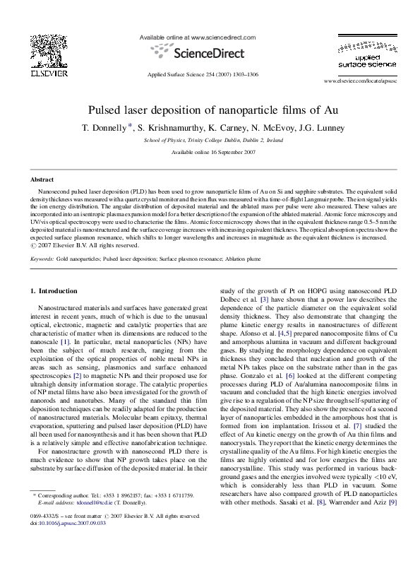
Fig. 3. AFM images for films of equivalent thickness (a) 0.5 nm, (b) 2.5 nm and (c) 4 nm Au on Si.
of the probe and deposition monitor, yields a value of
3.8 � 1012 ions cm�2 per shot at the position of the quartz
crystal monitor and substrate.
The mass lost from the target was measured to be 60 ng per
shot. This gives a value of 1.8 � 1014 for the total number of
evaporated particles which corresponds to an ablation depth of
2 nm per pulse. The angular distribution of the integrated ion
flux measured in the vertical plane is presented in Fig. 2. The
forward peaked nature of the ablation plume can clearly be seen
in this figure. The angular distribution was compared with the
isentropic gas dynamic expansion model of Anisimov by fitting
the data to the following equation [19]:
FðuÞ ¼ Fð0Þ
�
1 þ tan2 u
1 þ k2 tan2 u
�3=2
atoms (1.8 � 1014), but the reason for this discrepancy is not
clear at this stage.
For the synthesis of NP films the deposition monitor was
used to calculate the average deposition per shot (given above)
and the number of shots required was adjusted to give a desired
(1)
F(u) is the ion yield on a hemispherical surface as a function of
angle u measured from the target surface normal and k is the
aspect ratio of the plasma plume. Fitting the data using this
equation gives a value of k = 2.3. Using this k value and the
value for integrated ion flux normal to the target the Anisimov
model can be used to find the total number of ions in the plume.
Thus, we estimate the total number of ions in the plume to be
4.6 � 1014. This is somewhat larger than the number of ablated
Fig. 4. Optical absorption of 0.5 nm, 2.5 nm, 3 nm and 4 nm Au on Al2O3.
�1306
T. Donnelly et al. / Applied Surface Science 254 (2007) 1303–1306
equivalent thickness, which is the thickness obtained by dividing
the areal density of the film by the density of solid Au. Fig. 3
shows AFM images of 0.5, 2.5 and 4 nm thickness Au deposited
on Si. From the images we can see that in the case of 0.5 nm
equivalent thickness the Au nanoparticles have a height of 3 nm
and an apparent diameter of 66 nm. However, it seems that
apparent diameter is determined by the lateral spatial resolution
of the AFM. It can be seen that the coverage of the surface
increases with increasing equivalent thickness. Fig. 4 shows the
absorbance spectra of films prepared under the same conditions
but on sapphire and included is the absorption of a 3 nm film. It
can be seen that the absorption increases with increasing
equivalent thickness as expected. The surface plasmon resonance
(SPR) peak shifts to longer wavelengths with increasing
thickness which is consistent with our previous work on Ag
nanostructured films [12]. The SPR peak shifts from 550 nm for
the 0.5 nm film to about 770 nm for the 3 nm film.
4. Conclusion
In conclusion we have used PLD to deposit nanostructured
films of Au on Si and sapphire in vacuum. We have used a time
resolving Langmuir probe to characterise our deposition
plasma and have investigated how the film morphology and
optical absorption depends on the amount of material
deposited. From our analysis of the ablation plasma we have
found the average plume energy is 110 eV which is sufficient to
cause self-sputtering of the deposited material. Thin films of Au
have been deposited and below 5 nm equivalent thickness AFM
confirms the formation of NPs. As the equivalent thickness is
varied from 0.5 to 4 nm the NP size and surface coverage
increases. With increasing deposition the NPs coalesce until a
nearly continuous film exists for 4 nm equivalent thickness. The
optical measurements show the expected SPR feature which
increases in magnitude and shifts to longer wavelengths as the
equivalent thickness is increased.
Acknowledgment
This work was supported by the EU Specific Targeted
Research Project DESYGN-IT (No. NMP4-CT-2004-505626).
References
[1] F. Rosei, J. Phys.: Condens Matter. 16 (2004) S1373–S1436.
[2] E. Hutter, J.H. Fendler, Adv. Mater. 16 (2004) 19.
[3] R. Dolbec, E. Irissou, M. Chaker, D. Guay, F. Rosei, M.A. El Khakani,
Phys. Rev. B 70 (2004) 201406.
[4] C.N. Afonso, R. Serna, J.M. Ballesteros, A.K. Petford-Long, D.C. Doole,
Appl. Surf. Sci. 127–129 (1998) 339–343.
[5] C.N. Afonso, J. Gonzalo, R. Serna, J.C.G. de Sande, C. Ricolleau, C.
Grigis, M. Gandais, D.E. Hole, P.D. Townsend, Appl. Phys. A 69 (1999)
S201–S207.
[6] J. Gonzalo, A. Perea, D. Babonneau, C.N. Afonso, N. Beer, J.P. Barnes,
A.K. Petford-Long, D.E. Hole, P.D. Townsend, Phys. Rev. B 71 (2005)
125420.
[7] E. Irissou, B. Le Drogoff, M. Chaker, D. Guay, J. Appl. Phys. 94 (8) (2003)
4796–4802.
[8] T. Sasaki, N. Koshizaki, K.M. Beck, Appl. Phys. A 69 (1999) S771–
S774.
[9] J.M. Warrender, M.J. Aziz, Phys. Rev. B 75 (2007) 085433.
[10] B. Shin, M.J. Aziz, Phys. Rev. B 76 (2007) 085431.
[11] K. Seal, M.A. Nelson, Z.C. Ying, D.A. Genov, A.K. Sarychev, V.M.
Shalaev, Phys. Rev. B 67 (2003) 035318.
[12] T. Donnelly, B. Doggett, J.G. Lunney, Appl. Surf. Sci. 252 (2006) 4445–
4448.
[13] P. Ohresser, J. Shen, J. Barthel, M. Zheng, Ch.V. Mohan, M. Klaua, J.
Kirschner, Phys. Rev. B 59 (5) (1999) 3696.
[14] V. Dureuil, C. Ricolleau, M. Gandais, C. Grigis, J.P. Lacharme, A.
Naudon, J. Cryst. Growth 233 (2001) 737–748.
[15] J.I. Sohn, C. Nam, S. Lee, Appl. Surf. Sci. 197–198 (2002) 568–573.
[16] B. Toftmann, J. Schou, T.N. Hansen, J.G. Lunney, Phys. Rev. Lett. 84 (17)
(2000) 3998.
[17] S.I. Anisimov, D. Bauerle, B.S. Lukyanchuk, Phys. Rev. B 48 (16) (1993)
12076.
[18] S. Fahler, K. Sturm, H.U. Krebs, Appl. Phys. Lett. 75 (24) (1999)
3768.
[19] J.G. Lunney, B. Doggett, Proc. SPIE 6261 (2006) 62610B.
�
 Satheesh Krishnamurthy