111111111111111111111111111111111111111111111111111111111111111111111111111
US006387829Bl
(12)
(54)
(75)
(73)
United States Patent
(10)
Usenko et al.
(45)
SEPARATION PROCESS FOR SILICON-ONINSUIATOR WAFER FABRICATION
5,250,460
5,374,564
5,710,057
5,994,207
6,013,567
6,221,774
Inventors: Alexander Yuri Usenko, Murray Hill;
William Ned Carr, Montclair, both of
NJ (US)
Assignee: Silicon Wafer Technologies, Inc.,
Newark, NJ (US)
( * ) Notice:
Subject to any disclaimer, the term of this
patent is extended or adjusted under 35
U.s.c. 154(b) by 0 days.
(21)
Appl. No.: 09/543,998
(22)
Filed:
(60)
Related U.S. Application Data
Provisional application No. 60/139,851, filed on Jun. 18,
(51)
(52)
(58)
Int. CI?
U.S. CI
Field of Search
Apr. 6, 2000
1999.
(56)
HOiL 21/425; HOlL 21/265
438/977; 438/120
438/15, 977, 120
References Cited
U.S. PATENT DOCUMENTS
4,846,931 A
7/1989 Gmitter
Patent No.:
US 6,387,829 Bl
Date of Patent:
May 14,2002
A
A
A
A
A
B1
*
*
10/1993
12/1994
1/1998
11/1999
1/2000
4/2001
Yamagata
Brnel
Kenney
Henley et al.
Henley
Malik
438/515
438/690
* cited by examiner
Primary Examiner-Amir Zarabian
Assistant Examiner-Beth E. Owens
(74) Attorney, Agent, or Firm-DeMont & Breyer, LLC
(57)
ABSTRACT
A process for manufacturing a silicon-an-insulator wafer
from a silicon wafer assembly. The assembly is made of two
wafers. One of the wafers contains a fragile layer. The
fragile layer is a layer containing a high amount of hydrogen. An amount of energy from an energy source is applied
to the assembly to separate the assembly along the fragile
layer thus forming a silicon-on-insulator wafer and a leftover wafer. The energy source is selected from the group
consisting of: ultrasound, infrared, hydrostatic pressure,
hydrodynamic pressure, or mechanical energy. The amount
of energy is chosen to be sufficient to transform the fragile
layer into a quasi-continuous gaseous layer. Under separation the hydrogen-enriched layer transforms into layer consisting of hydrogen platelets and hydrogen microbubbles.
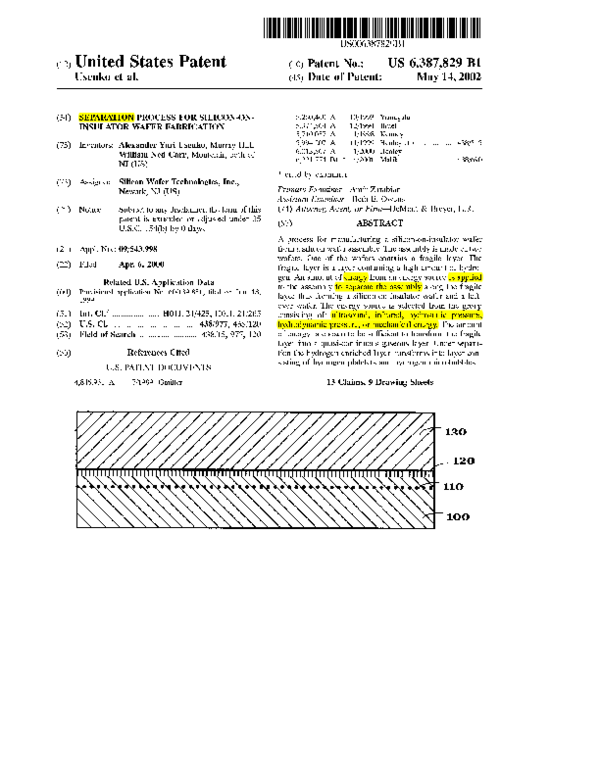
13 Claims, 9 Drawing Sheets
1::\0
120
110
100
�u.s. Patent
US 6,387,829 Bl
Sheet 1 of 9
May 14,2002
c
Fig.
L
L
セ
セ⦅
セ
セ
セ
セ
Mcセ
L
セ
セ⦅
セ
1.
Prior Art
__;r
Fig.
__;r
Fig. 3. Prior Art
:::l-
Fig. 4. Prior Art
__;r
2.
Prior Art
�u.s. Patent
セQPV
VPQセ|
May 14,2002
Sheet 2 of 9
US 6,387,829 Bl
601
rIO
L-----------------J
-----------------
60.1
Fig.5. Prior art
/,00
10
EXPANDING
CLEAVE
FRONT
Fig.6. Prior art
�u.s. Patent
[3
May 14,2002
Sheet 3 of 9
NfM M M M M セ
Fig. 7. Prior Art
Fig. 8. Prior Art
US 6,387,829 Bl
�u.s. Patent
May 14,2002
Sheet 4 of 9
US 6,387,829 Bl
Fig.9A
1:10
120
110
100
Fig.9B
セQPP
Fig.9C
�u.s.
Patent
May 14,2002
Sheet 5 of 9
.........•.•...••.•..........•.••...............
Fig. to
US 6,387,829 Bl
�u.s.
Patent
Sheet 6 of 9
May 14,2002
Fig.
11
US 6,387,829 Bl
�u.s.
Patent
Sheet 7 of 9
May 14,2002
121
120
Fig.l2A
Fig.12B
US 6,387,829 Bl
�u.s.
Patent
May 14,2002
Sheet 8 of 9
US 6,387,829 Bl
35
Fig.13A
Fig.13B
�u.s. Patent
May 14,2002
Sheet 9 of 9
Fig.l4A
14.2
l.p
140
Fig.14B
US 6,387,829 Bl
�US 6,387,829 Bl
1
2
patents on the ELTRAN process of fabrication of siliconon-insulator wafers. In this technique the film separation is
obtained by etching off a sacrificial layer comprised of
porous silicon.
This application claims priority from the provisional
patent application entitled "Separation Process For Silicon- 5
Still another variation of the epitaxial lift-off process for
On-Insulator Wafer" and, filed Jun. 18, 1999 and assigned
film separation is described by Kenney in U.S. Pat. No.
application No. 60/139,851, the disclosure of which is
5,710,057 [5]. In this technique an etchant distribution is
hereby incorporated incus entirety for all purposes.
facilitated by capillary action in trenches preformed in the
seed substrate.
BACKGROUND OF THE INVENTION
10
A disadvantage of the Bruel [lJ technique is that the
The present invention relates to the manufacture of
roughness of the as-cut surface requires polishing (e.g.,
silicon-on-insulator substrates. More particularly, the invenCMP) to smooth the surface. This polishing affects the
tion provides a technique for separating (cleaving) a subthickness uniformity of the device layer across the wafer.
strate as part of the fabrication process of silicon-onThus, the polishing process, while improving local
insulator wafers for semiconductor integrated circuits and 15 roughness, simultaneously increases thickness variations.
microelectromechanical systems.
Another disadvantage of the Bruel process [1 J is that the
assembly sometimes cleaves along an undesired plane. The
Delamination of thin films (micron range thickness) from
solids such as a single crystal is a processing step that is
desired plane is along the peak density of the implanted
useful for variety of technologies, including semiconductor
hydrogen. The undesirable plane is at a prebonded interface
processing technology. Prior art includes separation methods 20 between wafers of the assembly. Defective silicon-oninsulator wafers are the result.
as (1) ion cut with thermal initiation (Bruel), (2) ion cut with
jet initiation (Henley), and (3) variations of sacrificial layer
A disadvantage ofthe epitaxial lift-off technique [3J is that
etching (Gmitter, Yonehara, Kenney).
the area of delaminated film is limited to about 1 square inch,
The separation technique through a hydrogen-rich layer 25 that is much less that typical silicon wafer size (4-12 inches
was described by Bruel, U.S. Pat. No. 5,374,564 [1]. This
in diameter). So the process is not applicable to mainstream
technique is a part of Bruel's process [lJ used to fabricate
semiconductor processing.
silicon-on-insulator wafers. The technique uses thermal
A disadvantage of etch-stop based separation techniques
treating of a wafer assembly that includes a hydrogen[3,4,5J is the difficulty in obtaining a uniform layer thickness
implanted wafer. The annealing temperature used is above 30 for large areas. Since the etchant etches silicon in addition to
that at which ion implantation takes place. Typical annealing
the sacrificial layer, there is a tendency to reduce the
temperatures are in range from 400 to 500 0 C. Under
thickness at the thin film silicon near the outer perimeter of
annealing the implanted hydrogen begins to diffuse inside of
the wafer. The result is a separated thin film of decreasing
the wafer. Hydrogen coagulates into precipitates that serve
thickness along radii toward the wafer perimeter.
as nuclei for subsequent structure transfonnations. Then flat 35
Adisadvantage of the side jet technique [2J is that plasma
platelets consisting of hydrogen are formed from the nuclei.
immersion ion implantation dose needed in the process is
The platelets are arranged along <100> silicon crystallo10" 8 cm- 2 . Such a high dose severely deteriorates the quality
graphic planes. The platelets have top and bottom silicon
of the delaminated layer.
<100> surfaces with dangling bonds terminated by hydrogen. Next, bigger platelets continue to grow in expense of 40
SUMMARY OF THE INVENTION
smaller platelets according to the Ostvald ripening mechaA technique is detailed for forming a silicon film from a
nism. Finally, the continuous hydrogen layer is formed along
donor silicon substrate with <100> or <111> surface orienthe plane of the maximum implanted hydrogen. Following
tations.
annealing, the former single wafer is separated into two
45
A The technique utilizes a step of forming a hydrogen-rich
thinner wafers.
layer in a donor substrate at a selected depth underneath the
Another technique to delaminate a top layer from a silicon
surface where the hydrogen atoms have a relatively high
wafer using the buried hydrogen-rich layer is described by
concentration to define a donor substrate material above the
Henley in U.S. Pat. No. 6,013,567 [2]. The wafer is cleaved
selected depth. The hydrogen-rich layer may be obtained by
along the hydrogen-rich plane using a pressurized fluid jet
applied initially to the edge of the wafer. The cleavage 50 implanting hydrogen ions through a surface into the donor
wafer.
initiates at the edge due to the jet action and the cleavage
To initiate separation of thus prepared wafer, an energy
wave then propagates through the substrate to release a thin
source is applied to the substrate. The source is selected from
film of material from the substrate.
the group consisting of ultrasound, hydrostatic pressure,
Still another technique to selectively peel a film from a
single crystal is described by Gmitter in U.S. Pat. No. 55 hydrodynamic pressure, infrared light, mechanical, or combination thereof. Said energy source is applied in such a way
4,846,931 [3]. The technique is usually referred as epitaxial
that energy is deposited preferentially in the hydrogen-rich
lift-off. In this technique an epitaxial film is released from a
layer.
single crystal substrate upon which it is grown. The technique comprises (a) providing a thin release layer (1000 A)
The application of said energy source coagulates hydrobetween the film to be grown and the substrate; (b) growing 60 gen into nuclei having platelet shapes oriented along crysthe epitaxial film(s); (c) applying a polymeric support layer
tallographic cleavage planes, that is usually the <100> plane.
which is under tension over the film; and (d) selectively
The platelets then form a continuous layer thus releasing the
etching the release layer, the tension in the support layer
adjacent silicon film.
causing the edges of the film to curve upward as the release
For said ultrasound and infrared energy cases, choosing
layer is etched away.
65 preferable parameters means the wavelength is chosen
smaller than said donor substrate material thickness
A variation of the epitaxial lift-of process is described by
Yamagata in U.S. Pat. No. 5,250,460 [4J and subsequent
(typically less than 10 micrometers).
SEPARATION PROCESS FOR SILICON-ONINSUIATOR WAFER FABRICATION
�US 6,387,829 Bl
3
4
separation of a thin film from a single crystal silicon wafer
Advantage of the present invention is the technique adds
previously implanted with proton particles or with hydrogen
flexibility for creating customized silicon-on-insulator based
ions. The implanted wafer can be covered with thermally
microstructures and integrated circuits. Also the technique
grown silicon dioxide layer 105 (FIG. 9) before the implanrises the yield of silicon layer transfer as the hydrogen
platelet coagulation along the interface of prebonded silicon 5 tation stage. FIG. 9A is a simplified cross-sectional view of
the initial oxidized and wafer 100 implanted with protons
wafers is suppressed. Also the technique improves a surface
200 that form a hydrogen-rich layer 110 and a thin film to be
roughness of the silicon-on-insulator wafers obtained.
separated 120. FIG. 9B is a simplified cross-sectional view
diagram of the wafer 100 with a stiffener wafer 130 attached.
BRIEF DESCRIPTION OF THE DRAWINGS
This is an ioitial structure to be separated. FIG. 9C shows the
FIGS. 1 through 4 show prior art that is related to 10 final step of the separation process when the top assembly
consisting of stiffener wafer 130 and separated thin film 120
heat-caused separation [1].
is completely detached from initial implanted substrate 100.
FIG. 1 shows the concentration profile of the hydrogen
The process is used for the manufacture of silicon-onions as a function of the penetration depth.
insulator wafers from regular silicon wafers that are preFIG. 2 shows the monocrystalline semiconductor wafer 15 implanted with ions. The wafer undergoes an energy load
exposed to a bombardment of H+ ions and within which has
that transforms the pre-implanted layer into of a layer 110 of
appeared a gas microbubble layer produced by the implanted
gaseous microbubbles in the wafer. The wafer can be than
particles.
easy separated into two wafers along the layer of
FIG. 3 shows the semiconductor wafer of FIG. 2 and
microbubbles. In the FIG. 9A the implantation 200 occurs
20 through an upper surface of the wafer 100 that is substancovered with a stiffener.
tially parallel to a main crystallographic plane of the
FIG. 4 shows the cross-section view of assembly of the
substrate, for example the <100> plane. The implanted
semiconductor wafer and the stiffener wafer shown in FIG.
specie is preferably protons.
3 at the end ofthe separation phase, when cleaving has taken
The implantation allows for the formation of a layer of
place between the film and the substrate mass.
gaseous microblisters 110 within the volume of the wafer at
FIGS. 5 through 8 shows previous art that is related to 25 a depth approximately equal to the average ion penetration
jet-caused separation [2].
depth. This layer of microblisters delimits a surface layer
FIG. 5 is a simplified cross-sectional view of an implanted
120 within wafer 100, which will form the top part 120 of
substrate 10 using selective positioning of cleave energy
silicon-on-insulator wafer 140 in FIG. 9C. In particular, it
601.
30 should be noted that during ion implantation the wafer is
FIG. 6 illustrates the controlled-propagating cleave with
preferably kept at a temperature below the temperature at
which the atoms of the implanted gas can move away by
successive impulses 701, 705, 709 to initiate and then
propagate a cleariog process 700.
thermal diffusion from the crystaL
For all preferred embodiments described below, an
FIG. 7 shows a cross-sectional view of a pressurized fluid
jet from a fluid nozzle to perform a controlled cleaving 35 amount of energy from an energy source is applied to the
wafer assembly FIG. 9B. After applying the amount of
process.
energy a continuous hydrogen layer is formed at the place of
FIG. 8 shows a cross-sectional view of a pressurized fluid
the hydrogen-rich layer 110 thereby releasing silicon-onsource 607.
insulator wafer 150 (FIG. 9C) from byproduct wafer 100
FIG. 9 shows a cross-sectional view that illustrates the
40 (FIG. 9C.)
separation process due to present invention.
Preferred Embodiment 1: Separating with Ultrasound
FIG. 10 illustrates the first preferred embodiment of the
Energy Load
separation process due to the present invention where an
FIG. 10 shows the preferred embodiment utilizing ultraultrasound load is used.
sound as the activation energy for separation. The ultrasound
FIG. 11 illustrates the second preferred embodiment of 45 energy load is applied to the wafer assembly FIG. 9C
the separation process due to the present invention where a
through either the top or bottom surface.
hydrostatic pressure load is used.
For the separation, the implanted wafer is subjected to a
sensitizing load for a given time, chosen such that the
FIG. 12 illustrates the third preferred embodiment of the
hydrogen in the substrate which was introduced by the
separation process due to the present invention where infra50 hydrogen implantation is partly released from its attachred laser scanning is used.
ments to the defects (which were generated by the hydrogen
FIG. 13 illustrates the forth preferred embodiment of the
trap-inducing implantation) and as well by the hydrogen
separation process due to the present invention where a
implaimplantation itself. This treatment causes the formawater jet is used.
tion and growth of hydrogen filled microcracks at a depth
FIG. 14 illustrates the fifth preferred embodiment of the 55
close to the maximum in the concentration depth profile of
separation process due to the present invention where
implanted hydrogen. This step must not cause hydrogen
mechanical structures are used.
induced surface blisters, which would prevent subsequent
bonding of the first substrate to a second substrate.
DETAILED DESCRIPTION OF THE
At the end of energy activation the implanted hydrogen in
PREFERRED EMBODIMENTS
60 the substrate is fully released from chemical bonding to the
The present invention provides a technique for removing
defects. These defects were generated by the hydrogen
a thin film of material from a substrate while maintainiog the
trap-inducing implantation as well as by the hydrogen
structural integrity of both separated parts. Said thin film of
implantation itself, to cause growth, overlapping and coamaterial is prebonded to a stiffener, for example, an oxidized
lescence of hydrogen-filled microcracks, which split the
silicon wafer thus forming silicon-on-insulator wafer.
65 monocrystalline thin layer from the rest of the first substrate
The embodiments which will now be described in conthereby allowing the transferrance of the thin monocrystalline layer to the second substrate.
junction with the above drawings FIGS. 9 to 14, relate to the
�US 6,387,829 Bl
5
6
promoting hydrogen movement with formation of platelets
Ultrasound waves propagated through the bulk of a solid
94 (FIG. 10) affect the properties of point and extended
the similar way as it happens under heat treatment. The
defects. This processing is referred to as the process of
difference with the thermal treatment caused separation
ultrasound treatment. Ultrasound vibrations applied to a
described by Bruel is that the separation front is single and
semiconductor with a power density W, exceeding some 5 it propagates through the entire wafer. Finally it leaves
smoother surfaces after the separation as compared to a
threshold value, W rh are able either to generate Frenkel pairs
or to force the dissociation of complex centers composed of
multiple separation front case. Steps on the surface after
two or more point defects. The value ofW th was found to be
separation appear mostly at places where the two separation
of the order of 10 W/cm 3 . In the opposite case, i.e. when
fronts meet. Typical laser processing characteristics are:
W<W rh , a different effect related to the interaction of point 10 beam cross-section diameter 1 millimeter, laser pulse repetidefects and extended lattice defects has been found in single
tive rate 100 Hz, pulse duration 70 nanoseconds, horizontal
crystals. This effect of ultrasound is an enhancement of
scanning speed 50 mm/sec, energy per pulse 0.01 Joule,
gettering by sinks (dislocations, grain boundaries,
vertical scanning step 0.5 millimeters. In the case of using
precipitates) of both intrinsic and extrinsic point defects. The
the neodymium laser (wavelength 1.06 micrometer), the
ultrasound vibrations can reduce the energy barrier for the 15 silicon absorption coefficient is 50 cm- 1 for single crystal
silicon, and more than 103 cm- 1 for amorphous silicon. The
diffusion of defects as well as the barrier for their capture by
hydrogen-rich region has about the same absorption coeffisinks. The present invention uses the effect of the enhancecient as the amorphous silicon, so silicon bulk remains
ment of gettering by sinks, i.e. when W<Wrh"
In the preferred embodiment, ultrasound vibrations were
almost unheated, while the hydrogen-rich region melts at
generated in the wafer using a circular 100 mm diameter and 20 laser pulse energies higher than about 1 Joule/cm 2 . Pulsed
3 millimeter thickness piezoelectric transducer PZT-5A.
character of the laser processing is also important in this
case. For the nanosecond-range pulse duration the heat
Transducers were driven by a function generator and power
amplifier adjusted to the resonance frequency of the transproduced by the pulse dissipates during the pulse on disducer radial or thickness vibrations. For good acoustic
tances less than 1 micrometer, thus providing an adiabatic
contact, the wafer was pressed against a transducer front 25 mode of the processing. The pulsed laser treatment heats
predominantly the hydrogen-rich layer. In the heated layer
surface with a spring. The ultrasound transducer was operthe implanted interstitial hydrogen forms hydrogen clusters.
ated at resonance of its radial vibrations of 25 kHz. The
wafer assembly can be placed with either the stiffener or the
The clusters are nuclei of hydrogen platelets. Further heating
causes the nuclei of platelets to grow into bigger platelets.
cleavable surface to the transducer. The ultrasound load time
was 5 minutes or more (up to 120 minutes). The amplitude 30 Further, the growing platelets begin to overlap. The part of
of sample vibrations in acoustic contact with the transducer
the wafer assembly with the dense layer of platelets is a
was monitored by a calibrated contact acoustic probe. The
separated part. A border between separated and nonmaximum acoustic strain amplitude on the film surface was
separated parts is a separating front. The front moves
of the order of 10- 5 . The temperature of the sample under
following the scanning laser beam. FIG. 12B shows the
ultrasound load was stabilized at 50° c., and monitored by 35 different geometry of separation with pulsed infrared proa thermocouple attached to the wafer surface.
cessing where the entire wafer is processed in a single pulse.
Preferred Embodiment 2: Separating with Hydrostatic PresThis preferred embodiment is requires the high power laser
of a flash lamp source. The threshold energy for the sepasure Energy Load
ration is about 0.2 Joule/cm 2 , which translates into a 15
FIG. 11 shows the preferred embodiment using a hydrostatic pressure load to cause separation. The wafer assembly 40 Joule/pulse light source requirement for 100 mm diameter
31 is placed into hydrostatic pressure cell 111 and loaded
wafers.
with a pressure higher than 0.2 GPa. In silicon (and other
Preferred Embodiment 4: Separating with Hydrodynamic
Energy Source
diamond or zinc-blend structured materials), the diffusion
FIG. 13 shows the preferred embodiment utilizing a water
constant increases with pressure. This is in contrast with the
situation in close-packed materials in which diffusion dimin- 45 jet source to separate the donor substrate material. The water
jet nozzle 33 is initially aligned to the edge of the wafer
ishes with compression. Pressure cells, which use comassembly 31 to be separated. The wafer assembly consists of
pressed gas, can accommodate wafer size samples. The
implanted wafer 35 with hydrogen layer 36 and stiffener
compressed gas cells create a pressure up to 1.5 Gpa. This
wafer 37 attached to implantation side of the wafer 35. The
pressure is enough to cause separation of the silicon wafers.
Argon 112 is introduced into the cell 111 to approach 50 water jet nozzle moves with a speed of 0.01 to 0.1 cm/sec
hydrostatic conditions.
towards the center of the wafer assembly 31. The wafer
assembly is placed onto a supporting turntable that has a
Preferred Embodiment 3: Separating with Infrared Energy
spherical shaped surface with radius of curvature between 1
Load
and 2 meters. The turntable is made of material that has
FIG. 12 shows the preferred embodiment using an infrared energy source to cause separation. FIG. 12A illustrates 55 adequate rigidity, for example, stainless steel. The turntable
using of neodymium glass laser 120 in scanning mode. Said
is rotating with speed 0.1 to 10 rotations per second. The
laser produces a light beam 121 that is directed normally to
water jet beam trajectory on the wafer assembly 31 forms a
spiral 38 of continuously decreasing radius. The wafer
the surface of the wafer assembly 31 to be separated.
Scanning begins from the edge of said assembly 31 thus
assembly cleavage begins at the edge of the wafers. The
creating a separation front. The separation front propagates 60 cleaved part propagates inward with the jet and turntable
movements. The wafer assembly separates completely when
following the scanning laser beam. To complete separation,
an entire area of the wafer assembly 31 shoud be scanned.
the jet reaches the center of the wafer assembly 31. The
Said light wavelength should be chosen outside of the
typical water jet characteristics are: nozzle diameter of 1.6
silicon band edge absorption. If the energy of the photons is
millimeter, nozzle exit velocity 27 cm/sec (that gives a
lower than the forbidden gap, the photons are absorbed 65 corresponding Reynolds number Re=430). The nozzle diameter can vary from 0.1 to 2 millimeters, and the nozzle exit
mostly by defects. The hydrogen-rich layer is the defect-rich
and the light energy is absorbed mostly in this layer thus
velocity can vary from 10 to 100 cm/sec for typical wafer
�US 6,387,829 Bl
7
8
energy source selected from the group consisting of
configurations. Under the water jet action the wafer assembly 31 bends, the strain concentrates at the hydrogen-rich
ultrasound, infrared, hydrostatic pressure, hydrodylayer, thus encouraging the hydrogen atom movements
namiic pressure, mechanical, and a combination
inside the silicon. The displaced hydrogen forms platelets
thereof, wherein said amount of energy is sufficient to
the same way as under diffusion activation at elevated 5
transform said hydrogen-rich layer into a continuous
temperatures. The platelets form a continuous hydrogen
hydrogen layer thereby releasing said single-crystalline
layer that separates the wafer assembly 31 into two wafers
silicon layer.
with cleaving along the <100> preferred plane.
2. The process of claim 1, wherein said donor substrate is
Preferred Embodiment 5: Separating with Mechanical Linka silicon wafer.
10
ages and Structure
3. The process of claim 1, wherein said donor substrate
FIG. 14 shows the preferred embodiment applying
comprises single-crystalline silicon.
mechanical linkages and structure. FIG. 14A illustrates the
4. The process of claim 1, wherein said insulator layer
initial position when the wafer assembly 31 is placed onto
comprises
silicon dioxide.
anvil 140 and piston 141 is in its top position. Next, a
5. The process of claim 1, wherein said acceptor substrate
mechanical force 142 is applied to the piston and the piston 15
is single-crystalline silicon.
moves all the way down reaching its bottom position as
6. The process of claim 1, wherein said energy source is
shown on FIG. 14B. With this preferred embodiment the
ultrasound.
wafer assembly 31 bends and gets a shape predetermined by
7. The process of claim 6, wherein said ultrasound is a
said anvil 140 and piston 141. The bend gives the mechanical stress to the wafer and the stress promotes hydrogen 20 self-resonance mode ultrasound with an acoustic strain
amplitude of at least 10- 5 .
movement inside the wafer assembly 31 that has the
8. The process of claim 1, wherein said energy source is
hydrogen-rich layer. If the radii of curvature are chosen
properly, the wafer assembly gets stress that is not enough
an infrared energy source.
to break it in an unintentional place, but enough to separate
9. The process of claim 1, wherein said infrared energy
it along the weakened hydrogen-rich plane. The radii of 25 source provides infrared light that has a wavelength outside
curvature for the assembly is typically from 0.6 to 3 meters.
the silicon band edge absorption.
What is claimed is:
10. The process of claim 1, wherein said hydrostatic
1. A process for manufacturing a silicon-on-insulator
pressure energy source provides a hydrostatic pressure havwafer from a silicon wafer assembly, said process comprising an amplitude of at least 0.2 GPa.
ing the steps of:
30
11. The process of claim 1, wherein said hydrodynamic
providing a wafer assembly comprising a donor substrate
pressure energy source comprises a water jet.
having an insulator layer on a surface and a hydrogen12. The process of claim 1, wherein said mechanical
rich layer at a selected depth below said surface definsource comprises a structure to which a force may be applied
ing a single-crystalline silicon layer above said selected
in order to provide mechanical energy.
depth, and an acceptor substrate bonded to said surface 35
13. The process of claim 12, wherein said mechanical
for accepting said insulator layer and said singleenergy is applied to said structure which has a radius of
crystalline silicon layer above said selected depth, and;
curvature from about 0.6 to 3 meters.
applying to said wafer assembly an amount of energy
directed to a flat surface of said wafer assembly from an
* * * * *
�
 Alex Usenko