JOURNAL OF APPLIED PHYSICS 119, 174501 (2016)
Toward ultra high magnetic field sensitivity YBa2 Cu3 O72d nanowire based
superconducting quantum interference devices
M. Arzeo, R. Arpaia, R. Baghdadi, F. Lombardi, and T. Baucha)
Quantum Device Physics Laboratory, Department of Microtechnology and Nanoscience (MC2),
Chalmers University of Technology, SE-412 96 G€
oteborg, Sweden
(Received 8 January 2016; accepted 20 April 2016; published online 5 May 2016)
We report on measurements of YBa2Cu3O7�d nanowire based Superconducting QUantum
Interference Devices (nanoSQUIDs) directly coupled to an in-plane pick-up loop. The pick-up
loop, which is coupled predominantly via kinetic inductance to the SQUID loop, allows for a significant increase of the effective area of our devices. Its role is systematically investigated and the
increase in the effective area is successfully compared with numerical
pffiffiffiffiffiffi simulations. Large effective
areas, together with the ultra low white flux noise below 1 lU0 = Hz, make our nanoSQUIDs very
attractive as magnetic field sensors. Published by AIP Publishing.
[http://dx.doi.org/10.1063/1.4948477]
I. INTRODUCTION
Recent advances in nano-technologies applied to cuprate
High critical Temperature Superconductors (HTS) have made
it possible to realize nanowire based Superconducting
QUantum Interference Devices (nanoSQUIDs) with extremely
high magnetic flux sensitivity characterized by white flux
pffiffiffiffiffiffi
1=2
noise values SU below 1 lU0 = Hz.1,2 Such devices might
pave the way for the study of nano-magnetism at high magnetic fields with the ultimate goal of single spin detection.3
Here the high flux sensitivity is achieved by the small inductance of the SQUID loop.4 However, other prominent SQUID
applications, such as magneto encephalography5,6 and low
field magnetic resonance imaging,7 require a low magnetic
1=2
1=2
1=2
field noise, SB , which is given by SB ¼ SU =Aef f , with Aeff
the effective area of the device. In this respect, bare
nanoSQUIDs have a rather poor magnetic field sensitivity due
to their small loop area. In order to keep the low flux noise,
i.e., the small SQUID loop, one can increase the effective area
of the device by directly coupling the nanoSQUID loop to a
much larger pick-up loop. This approach has been already
employed for grain boundary Josephson junctions (JJs) based
HTS SQUID,8,9 and proven to allow for an at-will increase of
the effective area without altering the inductance of the
SQUID loop. Here it is important to note that such a feature is
not possible with the implementation of a SQUID washer,
where the SQUID inductance increases with the effective
area.10 Moreover, the simplicity of the single layer deposition
and single patterning process makes the pick-up loop approach
more attractive compared with an inductively coupled multiturn flux transformer. However, the noise mechanisms in
nanowire based SQUIDs as well as the effect of a pick-up
loop, coupled to this kind of nanoSQUID, on the overall noise
performance have not been previously studied.
In this work, we present results from the measurement
of YBa2Cu3O7�d (YBCO) nanoSQUIDs, realized in Dayem
a)
E-mail: thilo.bauch@chalmers.se
0021-8979/2016/119(17)/174501/5/$30.00
bridges configuration,1,11,12 directly coupled to an in-plane
magnetic field pick-up loop. The pick-up loop allows for a
significant increase of the effective area (Aeff) of our devices,
which is in a very good quantitative agreement with numerical calculations. Our calculations provide a more accurate
estimation of the effective area, in comparison with the
approximated expression commonly used in literature.9,10
The presence of the pick-up loop does not affect the magnetic
flux noise performances of our nanoSQUIDs with values for
pffiffiffiffiffiffi
the white flux noise below 1 lU0 = Hz. These devices are,
therefore, very appealing for future applications as magnetic
field detectors.
II. DEVICE LAYOUT AND FABRICATION
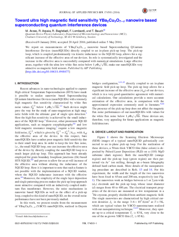
Figure 1 shows the Scanning Electron Microscope
(SEM) images of a typical nanoSQUID galvanically connected to an in-plane pick-up loop. For the realization of
these devices, a 50 nm thick YBCO film (false colors) is deposited by Pulsed Laser Deposition (PLD) on a (110) MgO
substrate (dark regions). Both the nanoSQUID (orange
region) and the pick-up loop (green region) are then patterned via Arþ ion milling, through an e-beam lithography
defined hard carbon mask. More details of the nanopatterning procedure are described in Refs. 13 and 14. For this
experiment, the width and the length of the two nanowires
have been fixed to 65 nm and 200 nm, respectively (see Fig.
1). The nanowires work as bridges between a 1 or 2 lm wide
(dw) electrode and the pick-up loop, whose inner diameter
(d) ranges from 40 to 400 lm. The electrical transport properties of the devices are measured at low temperature in a
3
He cryostat, properly shielded from ambient magnetic field.
The single nanowires are characterized by high critical current densities JC in the range 3–6 � 107 A/cm2 at T ¼ 5 K,
which are typical values for YBCO nanostructures realized
with our nanopatterning technique.14,15 Moreover, they operate up to a critical temperature Tc ’ 83 K, very close to the
one of the as grown YBCO film (Tc ’ 85 K).
119, 174501-1
Published by AIP Publishing.
�174501-2
Arzeo et al.
J. Appl. Phys. 119, 174501 (2016)
An analytic expression for the effective area, Aan
ef f , can
be obtained by means of an interacting loop-currents model
for superconducting networks in the presence of magnetic
field,16 satisfying the fluxoid quantization condition.17 Our
devices can be represented by an equivalent circuit as
sketched in Fig. 1(c), where the different parts act as inductive elements. By minimizing the total energy of the system
and keeping the vorticity of the pick-up loop at zero (number
of fluxoid quanta in the pick-up loop is zero), we get the following expression for the effective area:
pl
Aan
ef f ¼ AnS þ Aef f
FIG. 1. Scanning electron microscope images of a typical device. Here, the
YBCO is depicted in false colors (orange and green regions), whereas the
dark regions represent the MgO substrate. (a) Overview of the entire device, highlighting the shape and the size (diameter d and width w) of the
pick-up loop (green region). (b) Zoom-in, showing the details of the device
in the vicinity of the nanowires: a narrow electrode (orange) and part of
the pick-up loop (green), connected by the two nanowires, form the
nanoSQUID loop. The distance between the two wires and the width of the
pick-up loop in the vicinity of the nanowires are dw and wc, respectively.
(c) Circuit schematic of the presented devices. The different parts are represented by inductive elements. In particular, the nanowires are represented by the inductances L1nw and L2nw . The pick-up loop inductance is
given by the sum Lloop ¼ Lc þ L1loop þ L2loop and the nanoSQUID loop inductance by the sum L1nw þ L2nw þ Lc þ L1 þ L2 . The bias and the screening
current are denoted with Ib and Is, respectively.
III. RESULTS AND DISCUSSION
A. Effective area analysis
We first discuss the influence of the pick-up loop on
the effective area of the nanoSQUID. The effective area
represents the portion of the device that contributes to magnetic flux when an external magnetic field Ba is applied. It
can be experimentally determined from the measurement of
the modulation period DB of the SQUID’s voltage-field (or
critical current-field) characteristic, as expressed by the formula: Aexp
ef f ¼ U0 =DB, where U0 ¼ h=2e is the magnetic flux
quantum. The experimental effective area does not correspond to the nanoSQUID hole geometric area, which in our
specific case is given by the product of the separation
between the nanowires and their length l (see Fig. 1(b)):
Ageo ¼ dw � l. This is due to the fact that the total phase difference between the two wires is enhanced by the contribution of the superconducting phase gradient r/ induced by
the screening current Is circulating in the electrodes or, as
in this case, in the pick-up loop when an external magnetic
field is applied. This extra phase gradient is therefore responsible for an Aexp
ef f larger than Ageo.
Lc
;
Lloop
(1)
where AnS is the effective area of the nanoSQUID in absence
of the pick-up loop, Apl
ef f is one of the pick-up loops, and Lc
1
and Lloop ¼ Lc þ Lloop þ L2loop are, respectively, the coupling
and the total pick-up loop inductance (see Fig. 1(c)). The latter can be approximated using analytic expressions for a thin
superconducting film18
� � �
�
� �
l0 kL
t
l0
16r
0
�2
Lloop ¼
coth
ln
þ
kL
w
w
2p
� �
l kL
t
þ k=2;
(2)
L0c ¼ 0 coth
kL
wc
where l0 is the vacuum permeability, kL is the London penetration depth, t is the thickness of the YBCO film, w and r
are the average radius and width of the pick-up loop, respectively, and wc is the width of the YBCO strip where the two
loops meet (see Fig. 1(b)). Finally, k ’ 0.3 pH/lm is an empirical expression for a slit inductance per unit length,
obtained from measurements and simulations.19 The geometric term of L0c is, thence, approximated as half slit inductance. Here the prime sign indicates that Equations (2) are per
unit length. In both Equations (2), the first term is associated
to the kinetic energy of the charge carriers (kinetic inductance Lkin
i ) and the internal magnetic field energy, the second
one (geometric inductance Lex
i ), instead, to the energy from
the external magnetic field. Equation (1) infers that the coupling inductance Lc plays the major role, determining the
amount of magnetic flux transferred from the pick-up to the
nanoSQUID loop. For this reason, in order to enhance this
effect on the Aeff of the devices, the pick-up loop, in the
proximity of the nanowires, is 2 lm wide, whereas it widens
up to 10 lm over a distance of ’ 30 lm from them (see Fig.
1). Here, it is important to point out that for our devices the
kinetic contribution dominates over the geometric one.20
The geometric term, in fact, accounts only for roughly
34% of the total coupling inductance at T ¼ 5 K, becoming
even less significant at higher temperatures. Indeed, at
T ¼ 77 K, it accounts only for roughly 7% of Lc, with a ratio
ex
Lkin
c =Lc ’ 14 (see Fig. 2). This behavior in temperature
strongly indicates that the coupling between the nanoSQUID
and the pick-up loop takes place mainly via kinetic
inductance.
A more accurate estimation of the effective area of our
devices can be obtained by numerically solving the London
�174501-3
Arzeo et al.
and Maxwell equations21 in the presence of an externally
applied magnetic field Ba. The current distributions inside the
SQUID structure were calculated assuming the pick-up loop in
the zero flux state (zero vorticity) and, without loss of generality, zero circulating current in the small SQUID loop. The
effective area of the device can then be estimated from the
computation of the fluxoid value around the nanoSQUID loop,
0
U0 , and the applied field: Anum
ef f ¼ U =Ba . The temperature dependence can be taken into p
account
by using a modified twoffiffiffiffiffiffiffiffiffiffiffiffiffiffiffiffiffiffiffiffiffiffiffiffi
fluid model for kL ðTÞ ¼ k0 = 1 � ðT=Tc Þn , with n ’ 2.22
In Figure 2, we plot the experimentally determined
effective area Aexp
ef f versus the inner diameter (d) of the pickup loop, for devices with nanowires separation of 1 lm (orange circles) and 2 lm (green diamonds). In the same figure,
an
the solid and the dashed lines represent Anum
ef f and Aef f ,
respectively. As shown in the figure, the experimental data
are in a much better agreement with the numerical calculations compared with values obtained analytically using
Equations (1) and (2). This demonstrates that the numerical
method can be used for a more accurate and useful computational pre-study of any future device modification, regarding
both sizes and geometry, aiming at improved device performances. To perform the numerical simulations as
described, prior knowledge of the device dimensions and of
J. Appl. Phys. 119, 174501 (2016)
the London penetration depth value for our YBCO films is
required. The actual dimensions of each device have been
extracted from SEM images as illustrated in Refs. 13 and 15,
whereas we get the best fitting of the experimental data
shown in Fig. 2 using a k0 ’ 150 nm at T ¼ 5 K (kL
’ 400 nm, obtained from a modified two-fluid model with
Tc ¼ 83 K and n ¼ 2, is used for fitting data at T ¼ 77 K).
Such values differ from typical kL extracted for YBCO nanodevices.23,24 This could be due to the much larger lateral
dimensions of the pick-up loop and so of the entire device,
resulting in a kL comparable with the one for bulk YBCO.
On the contrary, any value of kL in the range 150–260 nm
does not allow for a good fitting of the experimental data by
means of Equations (1) and (2). This reflects an inaccuracy
in the analytic expression for the geometric inductances Lex
i .
The inaccuracy would be more pronounced for more complex geometries, for which the estimation of the geometric
inductances becomes very difficult.
B. Noise properties
We now focus on the characterization of the magnetic
flux noise of the devices. The noise measurements have been
performed in an open loop configuration and using a cross correlation scheme,25 which results in an amplifier input white
pffiffiffiffiffiffi
noise level of ’ 1:5 nV= Hz. The latter value also includes
the thermal noise from the resistive lines connecting the devices at low temperature to the room temperature amplifiers.
The nanoSQUIDs are biased by a DC current slightly above
the critical current (IC) and by an external magnetic flux,
which maximizes the value of @V=@U. The flux noise density
1=2
SU is evaluated from the measurement of the voltage noise
1=2
FIG. 2. Experimentally determined nanoSQUID effective area as a function
of the pick-up loop diameter, for devices with a wires separation of 1 lm (orange circles) and 2 lm (green diamonds) at T ¼ 5 K (a) and at T ¼ 77 K (b).
The solid and the dashed lines, representing, respectively, numerical and
analytic calculations, obtained for the different reported device geometries,
are presented for comparison. The extracted ratio between the kinetic and
geometric coupling inductance values increases from 2 at T ¼ 5 K to 14 at
T ¼ 77 K.
1=2
1=2
density SV as follows: SU ¼ SV =VU , where VU is the transfer function defined as: VU ¼ maxð@V=@UÞ. In Figure 3(b) we
show a typical spectral density of magnetic flux noise measured on a nanoSQUID, at T ¼ 5 K. In particular, the reported
measurement is taken at a DC bias current Ib ¼ 1.76 mA and a
flux bias such that VU ¼ 2.4 mV/U0, as shown in Figure 3(a).
The flux noise is, in fact, frequency dependent in the entire
pffiffiffiffiffiffi
range, with a value of about 100 lU0 = Hz at f ¼ 10 Hz. At
frequencies above 100 kHz, the flux noise is limited by the
1=2
electronics background noise. Therefore, we take SU ’
pffiffiffiffiffiffi
1 lU0 = Hz as the upper limit for the white noise of the device. This value is very close to the one previously reported
for equivalent YBCO nanoSQUIDs in the absence of the pickup loop.1 The f-dependent noise is not related to the flux bias
point, thence, it has to be attributed to the critical current fluctuations in our devices. Critical current fluctuations, in ordinary tunnel-like Josephson junctions (JJs), are usually
associated to bistable charge trapping states in the junction
barrier.26,27 In our nanowires instead, the critical current noise
might be caused by fluctuations of the electronic nematic
order.28,29 However, the detailed understanding of the physical
mechanisms responsible for such behavior in our nanowires is
not known yet and would require further systematic studies,
which goes well beyond the scope of the present work.
Nevertheless, for a more detailed and quantitative analysis of
the measured magnetic flux noise, we have fitted the spectra to
�174501-4
Arzeo et al.
J. Appl. Phys. 119, 174501 (2016)
contribution to the flux noise from critical current fluctuations
and extend the low noise region down to lower frequencies, one
would need a Flux-Locked Loop (FLL) configuration in combination with a bias reversal scheme.2,30 To study the influence of
the pick-up loop on the nanoSQUIDs noise performances, we
have characterized devices with different effective areas. In
Table I we report the measured values of the magnetic flux
white noise level, or the relative upper limit set by the read-out
electronics, for the investigated devices. A summary of the main
parameters for each nanoSQUID, including the dimensions and
the transport properties, are also listed in Table I. Our results
indicate that the white noise level is independent of the value of
the effective area of the device. This suggests that a further
increase of Aeff, by means of a bigger pick-up loop, will not
result in a deterioration of the noise performances. This would
allow the realization of nanoSQUIDs able to reach a magnetic
pffiffiffiffiffiffi
field sensitivity in the range of fT= Hz, which represents the
ultimate goal for various applications.5–7,31
IV. CONCLUSIONS
FIG. 3. (a) Voltage–flux characteristics at different DC bias currents and
temperature T ¼ 5 K. The dark red dot indicates the work point, at which the
spectrum is taken (Ib ¼ 1.76 mA), resulting in a transfer function
VU ¼ 2.4 mV/U0. (b) Magnetic flux noise spectral density SU as a function of
the frequency f, measured in an open loop configuration, at T ¼ 5 K, on a
nanoSQUID with dw ¼ 1 lm and coupled to a pick-up loop with an inner diameter equal to 100 lm (NSQ1, green line). The red solid line represents the
fit to F(f) as described in the main text. The spectrum due to the electronics
background noise is also plotted (blue line).
the sum of one or
1=2
1=2
more Lorentzians FL;i¼ F0;i =½1
1=2
þ ðf =fc;i Þ2 �1=2 with an amplitude F0;i and a characteristic fre1=2
quency fc,i, a contribution F1=f / 1=f 1=2 , and a constant white
noise term Fw1=2 . As shown in Figure 3(b), our data are very
pffiffiffiffiffiffiffiffiffiffiffiffiffiffiffiffiffiffiffiffiffiffiffiffiffiffiffiffiffiffiffiffiffiffiffiffiffi
well fitted by the expression F1=2 ðf Þ ¼ Ri FL;i þ F1=f þ Fw .
For the presented measurement, we have used two
1=2
Lorentzians, for which we extract fc;1 ¼ 25 Hz; F0;1 ¼ 80 lU0 =
pffiffiffiffiffiffi
pffiffiffiffiffiffi
1=2
Hz and fc,2 ¼ 200 kHz, F0;2 ¼ 1:4 lU0 = Hz, respectively,
pffiffiffiffiffiffi
and a white noise F1=2
w ¼ 0:8 lU0 = Hz. To remove the
We have fabricated YBCO nanoSQUIDs in Dayem
bridges configuration implementing high quality nanowires.
The electrical transport properties of these devices are characterized by a high reproducibility. The nanoSQUIDs are
directly coupled to an in-plane pick-up loop, which allows
for an at-will increase of the effective area of the devices.
The amount of magnetic flux transferred from the pick-up to
the nanoSQUID loop depends on the coupling inductance Lc.
In particular, the coupling takes place mainly via kinetic inductance as inferred from the temperature dependence of the
effective area. The influence of the pick-up loop, on both the
effective area and the noise performances, has been systematically investigated. The experimental determined effective
area has been successfully compared with numerical calculations based on the Maxwell and London equations. The
model can be further implemented to simulate the device
behavior with modifications in the design and dimensions.
The magnetic flux noise spectra for the investigated devices
are frequency dependent up to hundreds of kHz (limit set by
the read-out electronics bandwidth). This f-dependent noise
is attributed to critical current fluctuations and can be
described by the sum of Lorentzians, 1/f-like, and white
noise spectra. However, an important point is that the white
flux noise level of our nanoSQUIDs is independent of the
dimensions of the pick-up loop and, thence, of the effective
area. These results make our devices very attractive for
applications
requiring a magnetic field sensitivity in the
pffiffiffiffiffiffi
fT= Hz range, and thus a very large effective area. This
TABLE I. Parameters of some investigated nanoSQUIDs, characterized by different effective areas. The actual dimensions are obtained from SEM images of
the devices. VU is the value of the transfer function at the work point used for the noise measurement at T ¼ 5 K. IC and dR ¼ @V/@I are, respectively, the critical current and the differential resistance, extracted from the IV characteristics, with a voltage criterion of V ¼ 2 lV; SU,w is the magnetic flux white noise upper
limit of the device, as set by the electronics background noise. NSQR is a device without pick-up loop reported for comparison.1
Device
dw ðlmÞ
l (nm)
w (nm)
d ðlmÞ
Aeff ðlm2 Þ
IC ðmAÞ
dR ðXÞ
VU ðmV=U0 Þ
NSQ1
NSQ2
NSQR
1
1
1
200
200
100
65
65
65
100
400
…
24
62
2.8
1.7
2.4
1.75
0.8
2.4
0.2
2.4
0.75
1.5
pffiffiffiffiffiffi
1=2
SU;w ðlU0 = HzÞ
<1
<2
<1
pffiffiffiffiffiffi
1=2
SB;w ðpT= HzÞ
<86
<66
<740
�174501-5
Arzeo et al.
could be achieved by using larger coupling inductances and
a larger pick-up loop. As an example, increasing the pick-up
loop diameter by a factor of 20 (i.e., d ’ 8 mm) and the coupling inductancepLffiffiffiffiffiffi
c by a factor of 5 should result in a field
noise of 100 fT= Hz.
ACKNOWLEDGMENTS
This work has been partially supported by the Swedish
Research Council (VR) and the Knut and Alice Wallenberg
Foundation. We acknowledge support from the Marie Curie
Initial Training Action (ITN) Q-NET 264034.
1
R. Arpaia, M. Arzeo, S. Nawaz, S. Charpentier, F. Lombardi, and T.
Bauch, Appl. Phys. Lett. 104, 072603 (2014).
2
T. Schwarz, R. W€olbing, C. F. Reiche, B. M€
uller, M. J. Mart�ınez-P�erez, T.
M€uhl, B. B€uchner, R. Kleiner, and D. Koelle, Phys. Rev. Appl. 3, 044011
(2015).
3
C. Granata, A. Vettoliere, R. Russo, M. Fretto, N. De Leo, and V.
Lacquaniti, Appl. Phys. Lett. 103, 102602 (2013).
4
J. Gallop, Supercond. Sci. Technol. 16, 1575 (2003).
5
M. H€am€al€ainen, R. Hari, R. J. Ilmoniemi, J. Knuutila, and O. V.
Lounasmaa, Rev. Mod. Phys. 65, 413 (1993).
6
M. Xie, J. Schneiderman, M. Chukharkin, A. Kalabukhov, S. Whitmarsh, D.
Lundqvist, and D. Winkler, IEEE Trans. Appl. Supercond. 25, 1 (2015).
7
V. M. Zotev, A. N. Matlashov, P. L. Volegov, I. M. Savukov, M. A. Espy, J. C.
Mosher, J. J. Gomez, and R. H. Kraus, Jr., J. Magn. Reson. 194, 115 (2008).
8
M. Matsuda, Y. Murayama, S. Kiryu, N. Kasai, S. Kashiwaya, M.
Koyanagi, T. Endo, and S. Kuriki, IEEE Trans. Magn. 27, 3043 (1991).
9
D. Koelle, A. H. Miklich, F. Ludwig, E. Dantsker, D. T. Nemeth, and J.
Clarke, Appl. Phys. Lett. 63, 2271 (1993).
10
SQUID Sensors: Fundamentals, Fabrication and Application, Series E:
Applied Sciences Vol. 329, edited by H. Weinstock (Kluwer Academic
Publishers, 1996).
J. Appl. Phys. 119, 174501 (2016)
11
D. S. Hopkins, D. Pekker, P. M. Goldbart, and A. Bezryadin, Science 308,
1762 (2005).
12
C. Granata and A. Vettoliere, Phys. Rep. 614, 1 (2016).
13
R. Arpaia, S. Nawaz, F. Lombardi, and T. Bauch, IEEE Trans. Appl.
Supercond. 23, 1101505 (2013).
14
S. Nawaz, R. Arpaia, F. Lombardi, and T. Bauch, Phys. Rev. Lett. 110,
167004 (2013).
15
S. Nawaz, R. Arpaia, T. Bauch, and F. Lombardi, Physica C 495, 33
(2013).
16
C. C. Chi, P. Santhanam, and P. E. Bl€
ochl, J. Low Temp. Phys. 88, 163
(1992).
17
F. London, Superfluids (Wiley, 1950), Vol. 1.
18
T. Van Duzer and C. Turner, Principles of Superconductive Devices and
Circuits (Prentice Hall, 1999).
19
M. Ketchen, IEEE Trans. Magn. 27, 2916 (1991).
20
J. Johansson, K. Cedergren, T. Bauch, and F. Lombardi, Phys. Rev. B 79,
214513 (2009).
21
M. M. Khapaev, Supercond. Sci. Technol. 10, 389 (1997).
22
W. Rauch, E. Gornik, G. S€
olkner, A. A. Valenzuela, F. Fox, and H.
Behner, J. Appl. Phys. 73, 1866 (1993).
23
R. Arpaia, D. Golubev, R. Baghdadi, M. Arzeo, G. Kunakova, S.
Charpentier, S. Nawaz, F. Lombardi, and T. Bauch, Physica C 506, 165
(2014).
24
R. Arpaia, S. Charpentier, R. Toskovic, T. Bauch, and F. Lombardi,
Physica C 506, 184 (2014).
25
M. Sampietro, L. Fasoli, and G. Ferrari, Rev. Sci. Instrum. 70, 2520
(1999).
26
C. T. Rogers and R. A. Buhrman, Phys. Rev. Lett. 53, 1272 (1984).
27
D. Gustafsson, F. Lombardi, and T. Bauch, Phys. Rev. B 84, 184526
(2011).
28
Y. L. Loh, E. W. Carlson, and K. A. Dahmen, Phys. Rev. B 81, 224207
(2010).
29
E. W. Carlson and K. A. Dahmen, Nat. Commun. 2, 379 (2011).
30
D. Drung, Supercond. Sci. Technol. 16, 1320 (2003).
31
A. Chwala, J. P. Smit, R. Stolz, V. Zakosarenko, M. Schmelz, L. Fritzsch,
F. Bauer, M. Starkloff, and H.-G. Meyer, Supercond. Sci. Technol. 24,
125006 (2011).
�
 Riccardo Arpaia