B.Tech./EE-304 (Syllabus - 2017)
Class Test – II
(February 24, 2023)
(Electronics and Communication Engineering)
EE – 304 Electrical Network Theory
(3rd Semester)
Questions & Answers
✿✿✿✿✿✿✿✿✿✿✿✿✿✿✿✿✿✿✿✿✿✿✿✿✿✿✿✿✿✿✿
Duration: 1 hr.
Total Marks: 20
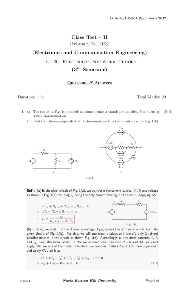
1. (a) The circuit in Fig. 1(a) models a common-emitter transistor amplifier. Find ix using
source transformation.
(b) Find the Thévenin equivalent at the terminals, a−b, in the circuit shown in Fig. 1(b).
+
−
2V
A
6Ω
b
βix
+
−
−
Ro
5Ω
A
23 V
vs +
−
2Ω
2V
Rs
+
−
ix
4Ω
−
a
+
18 V
10 V
a
b
Fig. 1
Soln .: (a) In the given circuit of Fig. 1(a), we transform the current source, βix into a voltage
as shown in Fig. 1(c) resulting ix being the only current flowing in the circuit. Applying KVL
ix
− vs + Rs ix + Ro ix + βRo ix = 0
⇒ (Rs + Ro + βRo ) ix = vs
vx
∴ ix =
Rs + (1 + β) Ro
Rs
Ro
+
−
+
vs −
βRo ix
Fig. 1(c)
(b) First of, we shall find the Thévenin voltage, VT H , across the terminals, a − b, from the
given circuit of Fig. 1(b). For this, we will use mesh analysis and identify only 3 (three)
possible meshes in the circuit as shown Fig. 1(d). Accordingly, all the mesh currents, i1 , i2
and i3 , have also been labeled in clock-wise directions. Because of 2 A and 3 A, we can’t
apply KVL on any of the mesh. Therefore, we combine meshes 2 and 3 to form supermesh
and apply KVL on it as
18 + 4(i2 − i1 ) + 6(i3 − i1 ) + 5i3 − 10 = 0
⇒ 4i2 + 11i3 − 10i1 + 8 = 0
20230224
North-Eastern Hill University
(1.1)
Page 1/6
[5+5]
�EE–304 ENT (Class Test - II)
Electronics and Communication Engineering
but we know that
+
−
2V
A
i1 = 2 A and i2 − i3 = 3 A
i1
Using above expressions in Eq. (1.1), we have
18 V
+
4Ω
6Ω
−
a
b
+
−
i3
A
23 V
5Ω
4(i3 + 3) + 11i3 = 12
∴ i3 = 0 A
2Ω
i2 2 V
+
−
−
and hence
10 V
i2 = 3 A
Fig. 1(d)
We now can find VT H from either
VT H = vab = 18 + v4 Ω + v6 Ω
= 18 + 4(i2 − i1 ) + 6(i3 − i1 )
= 18 + 4(3 − 2) + 6(0 − 2) = 18 + 4 − 12
= 10 V
or
VT H = vab = 10 + v5 Ω = 10 + 0 = 10 V
Next, we find RT H by suppressing all independent sources in the given circuit of Fig. 1(b)
resulting a resistive network as shown in Fig. 1(e). We know
+
−
2V
RT H = Rab = (R4 Ω + R6 Ω ) ||R5 Ω
= (4 + 6)||5
10 × 5
=
10 + 5
∴ RT H = 3.3333 Ω
4Ω
6Ω
a
b
+
−
We now draw the Thévenin equivalent of the
given circuit as below
2Ω
2V
5Ω
+
−
2V
Fig. 1(e)
RT H
a
3.3333 Ω
+
−
VT H
10 V
b
Fig. 1(f): Thévenin equivalent network of Fig. 1(b)
Alternative Solution
Above solution/equivalency can also be obtained by ✿✿✿✿✿✿✿✿
source ✿✿✿✿✿✿✿✿✿✿✿✿✿✿✿✿✿✿
transformation as
shown below:
2A
−
+
12 V
+
18 V
−
a
+
10 V
20230224
−
(4 + 6)Ω
+
30 V
a
10 Ω
−
2A
b
5Ω
b
2A
5Ω
⇒
North-Eastern Hill University
Page 2/6
�EE–304 ENT (Class Test - II)
Electronics and Communication Engineering
3A
3A
10 Ω
a
a
b
5Ω
b
3.3333 Ω
⇒
RT H
a
3.3333 Ω
+
−
VT H
+
a
3.3333 Ω
−
10 V
b
9.9999 V ≈ 10 V
b
⇒
Fig. 1(g): Thévenin equivalent network of Fig. 1(b) obtained using source transformation
2. Find voltage drop across the 4 Ω resistor in the circuit of Fig. 1(b) using superposition
principles.
Soln .: The given circuit of Fig. 1(b) redrawn as shown in Fig. 2(a)(i) by assigning the required
voltage, v4Ω to be determined. We have also drawn below other circuits in Fig. 2(a)(ii)2(a)(v), for applying superposition principles, wherein only 1 (one) independent source is
active at a time:
2A
+
+
10 V
v4Ω
3A
6Ω
4Ω
b
−
a
+
1
v4Ω
5Ω
18 V
6Ω
a
b
−
+
−
+
4Ω
4Ω
−
18 V
a
2A
+
5Ω
−
(i)
(iii)
+
3
v4Ω
3A
4Ω
6Ω
b
−
a
+
4
v4Ω
10 V
5Ω
+
4Ω
b
5Ω
(ii)
a
2
v4Ω
6Ω
−
6Ω
b
−
5Ω
−
(iv)
(v)
Fig. 2(a)
From Fig. 2(a)(ii) using the current division and Ohm’s law, we get
�
�
5
5
1
× −2 = −8 ×
= −2.6667 V
v4Ω = 4
(4 + 6) + 5
15
Again from Fig. 2(a)(iii) using the voltage divider, we have
2
v4Ω
=
4
4
× −18 = −18 ×
= −4.8 V
4 + (6 + 5)
15
And again from Fig. 2(a)(iv) using the current division and Ohm’s law, we get
�
�
6+5
11
3
v4Ω = 4
× 3 = 12 ×
= 8.8 V
4 + (6 + 5)
15
And lastly from Fig. 2(a)(v) using the voltage divider, we have
4
v4Ω
=
20230224
4
4
× 10 = 10 ×
= 2.6667 V
4 + (6 + 5)
15
North-Eastern Hill University
Page 3/6
[10]
�EE–304 ENT (Class Test - II)
Electronics and Communication Engineering
Therefore, the required voltage is given by superposition principles as
1
2
3
4
v4Ω = v4Ω
+ v4Ω
+ v4Ω
+ v4Ω
= −2.6667 − 4.8 + 8.8 + 2.6667 = 4 V
(2.1)
Verification
We will use Thévenin theorem to find the value of v4Ω . For this, we redraw the given circuit
of Fig. 1(b) as shown in Fig. 2(b)(iii). From this circuit, we remove the resistor, 4 Ω, and
find its equivalent Thévenin for the remaining network. Corresponding circuits to find VT H
and RT H are shown in Fig. 2(b)(iv) and Fig. 2(b)(v) respectively.
a
+
−
10 V +
−
18 V
18 V
a
+
18 V
+
−
a
4Ω
+
b
−
v4Ω
v4Ω
3A
6Ω
4Ω
2A
+
+
5Ω
b
b
(i)
4Ω
−
5Ω
−
v4Ω
2A 3A
6Ω
3A
−
10 V +
−
−
5Ω
10 V
+
2A
6Ω
(iii)
(ii)
a
+
18 V
−
a
RT H
+
+
−
10 V
11 Ω
2A 3A
VT H
5Ω
VT H
+
−
v4Ω
−5 V
5Ω
b
b
6Ω
6Ω
(iv)
4Ω
−
RT H
−
+
Network - A
(v)
Network - B
(vi)
Fig. 2(b)
To find VT H from Fig. 2(b)(iv), we shall use nodal analysis. Assigning node a as a reference
node, we apply KCL at node b as
vb − (−10)
−2+3=0
5
vb + 10
+1=0
⇒
5
⇒ vb = −15 V
∵ i6Ω = 3 A
Also vb being a node voltage with respect to the reference node a, we know
− vb = v5Ω + 10
⇒ v5Ω = −vb − 10 = 15 − 10 = 5 V
Now, we can find VT H as
VT H = −18 + 10 + v5Ω + v6Ω = −8 + 5 + 6 × 3 = −3 + 18 = 15 V
From Fig. 2(b)(v), we get
RT H = 5 + 6 = 11 Ω
Finally, the required voltage, v4Ω , is calculated using voltage division from the circuit of
Fig. 2(b)(vi) as
v4Ω =
4
× 15 = 4 V
4 + 11
which ✿✿✿✿✿✿✿✿
matches✿✿✿✿✿
with✿✿✿✿✿
that✿✿✿
of ✿✿✿✿
Eq.✿✿✿✿✿✿
(2.1).✿✿✿✿✿✿✿✿
Hence, ✿✿✿✿
the ✿✿✿✿✿✿
result ✿✿
is✿✿✿✿✿✿✿✿
verified.
20230224
North-Eastern Hill University
Page 4/6
�EE–304 ENT (Class Test - II)
Electronics and Communication Engineering
[5+5]
2 V11′
+
4Ω
1
−
3. For the circuit of Fig. 2, obtain
(a) V11′ using superposition principles, and
+
(b) The Norton equivalent at terminals, 1 − 1′ .
5V +
−
3A
V11′
−
1′
Fig. 2
Soln .: (a) The given circuit of Fig. 2 is redrawn by making only one independent source
active at a time as shown below. Let V11′ = V111 ′ + V112 ′ where V111 ′ and V112 ′ are voltages
due to the 5V and 3A sources when acted one at a time respectively.
+
5V +
−
1
1
+
V111 ′
−
2 V112 ′
+
−
+
4Ω
−
2 V111 ′
4Ω
V112 ′
3A
−
1′
1′
(ii)
(i)
Fig. 3(a)
From Fig. 3(a)(i) by KVL, we have
− 5 + 4 × 0 + 2V111 ′ + V111 ′ = 0
5
⇒ V111 ′ = = 1.6667 V
3
∵ i4 Ω = 0 A
Applying KVL in From Fig. 3(a)(ii), we have
4 × (−3) + 2V112 ′ + V112 ′ = 0
12
=4V
⇒ V112 ′ =
3
Therefore, the required voltage is
V11′ = V111 ′ + V112 ′ = 1.6667 + 4 = 5.6667 V
(b) We first find Norton current, IN , by shorting the terminals, 1 − 1′ , in the circuit of
Fig. 3(b)(i), which in turn makes the 3A source shorted. Therefore, V11′ = 0 V.
+
−
+
5V +
−
3A
V11′
1
2 V11′
1V
−
−
1′
(ii)
(i)
+
−
V11′
V11′
1′
1
+ itest
+
IN
− IN
I1
4Ω
2 V11′
4Ω
+
1
−
+
2 V11′
−
4Ω
1′
(iii)
Fig. 3(b)
Applying KVL in the perimeter (outer loop) of the circuit, we have
− 5 + 4I1 + 2V11′ = 0
5
⇒ I1 = = 1.25 A ∵ V11′ = 0 V as both terminals are shorted
4
We also know
IN − I1 = 3
⇒ IN = 3 + I1 = 3 + 1.25 = 4.25 A
20230224
North-Eastern Hill University
Page 5/6
�EE–304 ENT (Class Test - II)
Electronics and Communication Engineering
Now, for RT H , we use an external 1V voltage source as shown in Fig. 3(b)(iii). Applying
KVL in the circuit, we have
a
4 × −itest + 2V11′ + 1 = 0
⇒ − 4itest + 2 + 1 = 0 ∵ V11′ = 1 V
3
∴ itest = = 0.75 A
4
IN
4.25 A
RN
1.3333 Ω
b
Fig. 3(c): Norton equivalent network of Fig. 2
Hence, the Norton resistance, RN , is given by
RN =
20230224
1
1V
=
= 1.3333 Ω
itest
0.75
North-Eastern Hill University
Page 6/6
�
 Joyprakash Lairenlakpam