A Comparison of Single Junction and Transistor Structure Solar Cells
Stephen C. Pritchard, Keith R. McIntosh, Pietro P. Altermatt, Christiana B. Honsberg
Photovoltaics Special Research Centre
University of New South Wales
Sydney NSW 2052
AUSTRALIA
Telephone:
+61 (0)2 9385 4018
Facsimile:
+61 (0)2 9662 4240
Abstract
Despite the predominance of single junction solar cells, both in research and commercial production,
triode or transistor structure solar cells offer performance advantages on a range of substrate materials.
This paper uses the semiconductor device simulator PC1D to compare a single junction silicon solar
cell with two silicon transistor structures, in order to quantify the expected performance increases, and
to show how minority carrier diffusion length and wafer thickness influence these relative advantages.
1
INTRODUCTION
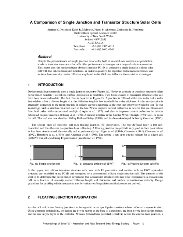
Device modelling commonly uses a single junction structure (Figure 1a). However, a triode or transistor structure offers
performance benefits if a realistic surface passivation is modelled. Two broad classes of transistor structure solar cell
have been examined to date. The first class is depicted in Figure 1b. A junction is diffused at the rear surface of a wafer
that exhibits a low diffusion length - i.e. the diffusion length is less than half the wafer thickness. As this rear junction is
externally connected to the front junction, it collects carriers generated at the rear that otherwise would be lost. To our
knowledge, such a structure was first used in the late 70's to improve current collection in devices that are illuminated
from both sides with concentrated sunlight (Luque et al. 1977), and also to improve current collection in devices
fabricated on poor materials (Chiang et al. 1978). A similar structure is the Emitter Wrap-Through (EWT) cell, or polka
dot cell. This cell was described in 1980 by Hall and Soltys (1980), and has been developed further by Gee et al, (1993).
The second class of transistor cell uses floating junction (FJ) passivation. The rear diffused layer is left noncontacted, and thus the rear p-n junction bias is floating. A floating junction can provide very good surface passivation,
as has been demonstrated theoretically and experimentally by Lölgen et al. (1994), Ghannam (1991), Ghannam et al.
(1992), Honsberg et al. (1994), and Altermatt et al. (1996). The record 1-sun open circuit voltage for a silicon cell
(720mV) was achieved using FJ passivation (Wenham et al, 1994).
E
E
B
E
B
B
Fig. 1a: Single junction cell
Fig. 1b: Wrapped emitter cell (EWT)
Fig. 1c: Floating junction cell (FJ)
In this paper, two silicon transistor structure cells, one with FJ passivation and another with an EWT equivalent
structure, are modelled using PC1D and compared to a conventional silicon single junction cell. The purpose of this
work is to determine the performance advantages that a transistor structure cell may offer compared to a conventional
cell, as a function of minority carrier diffusion length, cell thickness, and surface recombination velocity. Design
guidelines for deciding which structure to use for various wafer qualities and thicknesses are derived.
2
FLOATING JUNCTION PASSIVATION
A solar cell with a rear floating junction can be regarded as an npn bipolar transistor whose collector is open-circuited.
Using common terminology, we denote the p-type region as the base of a transistor, the front n-type layer as the emitter,
and the rear n-type layer as the collector. When a forward bias potential is built up across the emitter-base junction, a
Proceedings of Solar ’97 - Australian and New Zealand Solar Energy Society
Paper 112
�A Comparison of Single Junction and Transistor Structure Solar Cells
S. Pritchard et al
similar potential is induced in the rear junction, provided that the wafer material has a diffusion length of at least the cell
thickness. This implies that the concentration of electrons at the rear of the base is higher in a floating junction than in a
single junction device, under identical operation conditions. Consequently, the electron current diffusing towards the
rear surface is reduced in the FJ cell and this effectively reduces the rear surface recombination velocity (Ebong et al,
1997). In addition, it has been shown that passivation by a thermally grown oxide is more effective at n-type surfaces
than at p-type surfaces (Green, 1995) which is a further benefit of the FJ passivation.
3
‘EMITTER WRAP-THROUGH’ CELLS
In cells equivalent to the emitter wrap-through (EWT) structure, the collector is contacted to the emitter and thus is not
floating. This connection can be made internally via dopants diffused in holes through the cell, so that both positive and
negative contacts can be placed on the rear. Alternatively, the emitter-collector connection may be made externally by
contacting both the front and the rear of the cell. Since the differences between these two connection schemes are not
apparent in one-dimensional simulations, we treat the two structures as equivalent.
EWT cells afford better rear surface passivation than single junction devices due to the n-type layer at the rear. Ideally,
an EWT cell does not incur the same fill factor losses that are incurred in an oxide passivated single junction cell with
an injection level dependent rear surface recombination velocity (Aberle et al, 1993). However, EWT cells may suffer
from a reduced open circuit voltage. This is because there is a net current flow across both the front and rear junction, so
the junction area of an EWT cell is effectively twice that of either a single junction or a floating junction solar cell.
Doubling the junction area doubles the saturation current component due to SRH recombination in the base and emitter.
Thus, if the bulk region of the cell is the predominant site of recombination, rather than the surfaces, the EWT cell has a
lower open-circuit voltage relative to a single junction or FJ cell. However, when surface recombination limits the
energy conversion efficiency, as is the case in cells with long diffusion lengths, small device widths, or high surface
recombination velocities, the open-circuit voltage of the EWT cell is competitive with that of other cells.
4
MODELLING THE DEVICES WITH PC1D
We used the software PC1D (Basore & Clugston, 1996) to model the three structures under AM1.5G illumination from
the front. Cell thickness was varied from 100 µm to 800 µm, and the diffusion lengths were varied from 50 µm to 1000
µm by changing minority carrier lifetimes. For comparison, the surface recombination velocity is always set to 1000
cm/s at both the front and the rear of the cell. This value is an experimental estimate of the rear surface recombination
velocity in cells with an aluminium-sintered back surface field, which is a common rear surface passivation option for
single junction devices. The emitter and collector have the same doping profile, representing a possible commercial
fabrication where the two are diffused simultaneously. Other parameters are chosen to approximate experimental buried
contact single junction and FJ devices. An internal short circuit from the front to the rear of the cell is included in the
EWT cell. Common device parameters for the three structures are listed in Table 1. For the Si parameters, such as band
gap narrowing etc, we chose the default values given in PC1D.
Maximum light trapping (i.e. 99 % internal and no external reflection) is chosen to ensure that the influence of the rear
p-n junction is emphasized in the trends of Jsc and η for various thicknesses and diffusion lengths. This accounts for the
higher than experimentally measured short-circuit currents and efficiencies. Parasitic resistance effects are not included
in order to keep any conclusions general. The modelled open circuit voltages provide a good match for both
experimental single junction and floating junction devices. Our intention is to identify the relative advantages and
disadvantages of the different structures, not to simulate a cell with a very high efficiency.
Table 1: Common Device Parameters
p-type background doping density
Peak-doping density in n-type diffusions
Junction depths (front and rear)
Doping profiles (front and rear)
SRV (electrons and holes, p- and n-type)
2
1.41e+016 cm-3
5.00e+018 cm-3
1 µm
Gaussian
1000 cm/s
Proceedings of Solar ’97 - Australian and New Zealand Solar Energy Society
Paper 112
�A Comparison of Single Junction and Transistor Structure Solar Cells
5
S. Pritchard et al
RESULTS
The results obtained give an indication of the relative advantage a rear junction offers for some substrate materials and
wafer thicknesses.
690
615
610
Single Junction
FJ
680
EWT
Single Junc tion
FJ
EW T
605
600
Voc (mV)
Voc (mV)
670
595
590
660
650
585
640
580
575
630
0
1
2
3
4
5
6
7
Thickness/Diffusion Length (W/L)
Figure 2a - Open circuit voltage for L = 100 µm
8
9
0.0
0.2
0.4
0.6
0.8
1.0
1.2
1.4
1.6
1.8
Thickness/Diffusion Length (W /L)
Figure 2b - Open circuit voltage for L = 500 µm
Figure 2a displays the modelled open circuit voltage (Voc) of the three cell structures, using a substrate diffusion length
(L) of 100 µm, over wafer thicknesses (W) ranging from 100 µm to 800 µm. Voc of the single junction cell is insensitive
to cell thickness if the latter is larger than three times the diffusion length. This is because the electrons generated at the
rear of the cell recombine there, and do not affect the voltage across the emitter-base junction (which is measured as
Voc).
The floating junction cell exhibits an almost identical Voc to the single junction cell in the 100 µm diffusion length case,
again demonstrating the unimportance of recombination at the rear surface for W/L ratios greater than 3. When W/L is
less than 2, however, the FJ cell has a higher Voc than the single junction cell, indicating the transition region where the
predominant recombination mechanism shifts from bulk recombination to surface recombination, and the superior rear
surface passivation of the FJ cell becomes important.
As expected, the Voc of the EWT cell is always lower than that of the floating junction solar cell, and lower than the
single junction solar cell if W/L is greater than approximately 1.2. For very large W/L, the EWT open circuit voltage
approaches a value approximately 18 mV less than that of the other cells. This difference arises from the effectively
doubled junction area in the EWT device. When the devices are limited by bulk recombination, the EWT device
effectively has twice the bulk region in which carriers that could be collected will recombine.
However, when W/L is reduced, the Voc of the EWT cell rises faster relative to the other two cells and surpasses the Voc
of the single junction cell when W/L is roughly 1.2. This trend is more evident in simulations we have performed using
longer diffusion lengths. The reason for this is that the point at which surface recombination begins to dominate occurs
at a larger W/L ratio in the EWT cell due to its capacity to collect carriers from the rear of the bulk region. These
carriers would only have a slim chance of being collected in the other two cells. We see in Figure 2a that the open circuit
voltage of the EWT cell begins rising significantly when W/L is just less than 4. The open circuit voltages of the other
two cells do not begin rising at a similar rate until W/L is less than 2.
Figure 2b displays the simulated Voc on wafers with diffusion lengths of 500 µm over the same range of device
thicknesses as the shorter diffusion length case. At these smaller W/L ratios, the trends in Voc for the transistor structure
cells are similar to Figure 2a, i.e. Voc increases as the thickness is reduced. For very small W/L (less than 0.4) the EWT
cell has a similar Voc to the FJ cell. This indicates that recombination within the devices is occurring predominantly at
the surfaces, since we do not see a significant drop in Voc due to the extra bulk recombination associated with the second
emitter in the EWT cell.
The single junction cell exhibits a different trend in Voc than in Figure 2a. Its Voc decreases as cell thickness is reduced.
In contrast to Figure 2a, bulk recombination is less significant, and so good surface passivation is highly beneficial. The
rear surface passivation of the single junction cell is not as effective as that in the transistor structure cells, and the rear
surface recombination losses outweigh any decrease in bulk recombination resulting from a thinner wafer.
Proceedings of Solar ’97 - Australian and New Zealand Solar Energy Society
Paper 112
3
�A Comparison of Single Junction and Transistor Structure Solar Cells
44.0
43
43.5
42
Single Junction
FJ
EWT
43.0
41
Jsc (mA/cm2)
Jsc (mA/cm2)
S. Pritchard et al
40
39
42.5
42.0
38
41.5
37
41.0
36
Single Junc tion
FJ
EW T
0.8
1.0
40.5
0
1
2
3
4
5
6
7
Thickness/Diffusion Length (W/L)
Figure 3a - Short circuit current for L = 100 µm
8
9
0.0
0.2
0.4
0.6
1.2
1.4
1.6
1.8
Thickness/Diffusion Length (W /L)
Figure 3b - Short circuit current for L = 500 µm
Figure 3a depicts the simulated short circuit current density (Jsc) of each cell for a substrate diffusion length of 100 µm,
over cell thicknesses ranging from 100 µm to 800 µm. The single junction cell displays a rising Jsc as W/L is reduced.
This is expected when the high level of light trapping is taken into account. In thinner cells, generated carriers do not
need to travel as far in order to be collected, and current collection is increased.
Figure 3a also displays the similarity in Jsc response between the floating junction cell and the single junction cell when
W/L is large. The two cells are identical when W/L is large, since the improved surface passivation of the FJ cell only
impacts upon carriers at the rear of the device, which are not collected by the front junction regardless. Once W/L is
reduced below approximately 2, Jsc of the FJ cell improves relative to the single junction cell.
The EWT cell exhibits higher short circuit current densities than either of the other cells, as the rear collecting junction
of the EWT cell can collect carriers that are generated one diffusion length from the rear. The current collection
advantage of the EWT is maximized when W/L equals 2, for at this ratio the current collection capability of the single
junction and FJ cells is eroded and carriers generated in the bottom half of the cells are unlikely to be collected by the
front emitter. The EWT though is able to collect these carriers at the rear emitter. When W/L is smaller than 2, all three
structures exhibit good current collection, and carriers generated near the rear of the cell are able to diffuse to the front
collecting junction in the single junction or FJ cells. As W/L decreases, the Jsc of all cells approach the same value as
seen in Figure 3b. For W/L larger than 2 the number of carriers generated one diffusion length from the rear junction
decreases, and therefore the inclusion of a rear collecting junction becomes less advantageous. The Jsc response of the
EWT cell approaches that of the other cells when W/L becomes very large.
The case with 500 µm diffusion length is displayed in Figure 3b. The single junction still shows a trend for Jsc to
increase as thickness is reduced, however it does not increase as fast as the Jsc of the floating junction cell, due to the
extra recombination incurred at the rear surface of the single junction cell. In fact the FJ short circuit current density has
increased significantly faster than either cell, and is almost level with the EWT cell when W/L is less than 0.3. We
deduce from this that the mechanism that limits the short circuit current density on these thin, high quality wafers is
recombination at the rear surface. The EWT cell does not gain much advantage with its second emitter over the FJ cell,
indicating that all three cells are capable of collecting carriers generated at all depths.
The downturn in Jsc for the transistor structure cells when W/L ratios are small occurs only for very high short circuit
current densities (greater than 43mA/cm2 in these simulations) and only for very thin devices, when W/L is less than
approximately 0.6. This decrease in Jsc is caused by the greater influence of surface recombination in very thin, heavily
light trapped devices.
Having identified trends in Voc and Jsc, trends in efficiency can be understood. Figures 4a and 4b illustrate the results for
the 100 µm diffusion length case and 500 µm diffusion length case, respectively, over thicknesses ranging from 100 µm
to 800 µm.
When W/L is very large, we again see the insignificance of effective rear surface recombination velocity in the single
junction and FJ cells through their identical performance. The FJ cell only begins to generate power more efficiently
than the single junction cell when W/L is less than 2. Both cells experience an increase in efficiency as W/L is reduced
for the poor diffusion length case, in keeping with the voltage and current density results.
4
Proceedings of Solar ’97 - Australian and New Zealand Solar Energy Society
Paper 112
�A Comparison of Single Junction and Transistor Structure Solar Cells
25.0
21.5
21.0
S ingle Junction
24.5
Single Junction
20.5
FJ
FJ
EW T
EWT
24.0
Efficiency (%)
Efficiency (%)
S. Pritchard et al
20.0
19.5
19.0
23.5
23.0
22.5
18.5
22.0
18.0
17.5
21.5
0
1
2
3
4
5
6
Thickness/Diffusion Length (W/L)
Figure 4a - Efficiency for L = 100 µm
7
8
9
0.0
0.2
0.4
0.6
0.8
1.0
1.2
1.4
1.6
1.8
Thickness/Diffusion Length (W /L)
Figure 4b - Efficiency for L = 500 µm
Figure 4a shows that there is a crossover point where the EWT cell changes from achieving a superior to an inferior
efficiency, which occurs at an W/L ratio between 4 and 5. For large W/L ratios, the current collection advantage of the
EWT cell becomes less significant, and this combined with the lower Voc when W/L is large results in the EWT
performing worse than either of the other cells. For smaller W/L ratios, the current collection advantage of the EWT cell
gives it improved efficiency over the other cells, and at the same time the loss in Voc caused by extra recombination
resulting from the second emitter is not so significant. The EWT cell achieves an optimum balance between improved
current collection and improved voltage relative to the other cells when W/L is between approximately 1 and 2. In this
range, the EWT cell has a maximum efficiency advantage over the other structures. This range of maximum advantage is
even more evident in other simulations using substrate diffusion lengths of 200, 300 and 400 microns.
Figure 4b illustrates the superior performance of the transistor structure cells when W/L is small. The single junction cell
is limited by an open circuit voltage that falls when thickness is reduced due to its high rear surface recombination
velocity, and its performance does not greatly improve as thickness is reduced despite increased current collection. The
EWT generally performs better than the FJ cell and both structures experience an increasing efficiency as thickness is
reduced. However, when W/L is very small, less than 0.3, the floating junction cell is just as efficient as the EWT. The
current collection advantage of the EWT is minimal for W/L less than 0.3 since diffusion lengths are long compared to
device width and most carriers generated in the rear of the bulk region are able to diffuse all the way to the front and be
collected regardless.
It must be pointed out that these results are idealized, and experimental devices may show performance variations that
may alter the relative advantages or disadvantages of each structure. For example when series resistance losses are
included, it is likely that the Emitter Wrap-Through cell could perform better relative to the other cells for small W/L
ratios, due to its resilience to high emitter sheet resistance losses. An increased sheet resistance in one emitter simply
means that injection will be greater at the other junction. Koschier (1994) has modelled double junction cells and shown
the increased insensitivity of double junction and other multi-junction structures to series resistance effects. Another
generalization made here is that a surface recombination velocity of 1000cm/s was assumed at all surfaces, n- and ptype. This was done to provide uniformity between the different structures in order to analyze performance differences
arising solely from the effects that a rear n-type layer has on effective rear SRVs and current collection. In reality, the
SRV at an n-type surface is likely to be lower than this, so the two transistor structures do not achieve their full potential
relative to a conventional device in our simulations. Finally, parasitic shunting of the rear n-type layer is not included in
our model, an effect that can limit the effectiveness of a fabricated transistor structure cell (Wenham et al, 1994,
Altermatt et al. 1996). This shunting can be minimized through biasing the rear junction by illuminating the rear side of
the cell, or, more generally, by increasing the sheet resistivity of the rear n-type layer. Increasing the sheet resistivity
isolates the regions of low bias and high surface recombination velocity that result from shunting, thereby allowing good
passivation over most of the rear surface (Honsberg et al, 1996).
6
CONCLUSIONS
It has been shown that transistor structure solar cells can achieve higher open circuit voltages, short circuit current
densities, and energy conversion efficiencies than conventional devices on a wide range of silicon wafer qualities and
thicknesses. The Emitter Wrap-Through equivalent structure achieves its greatest advantage over the other structures on
wafers with a thickness/diffusion length ratio between 1 and 2. For ratios much smaller than 0.5, it is preferable to use a
Floating Junction structure, since a cell with this structure performs just as well as an EWT structure on these wafers,
and requires fewer processing steps to fabricate. On wafers with W/L ratios much greater than 3, neither of the transistor
Proceedings of Solar ’97 - Australian and New Zealand Solar Energy Society
Paper 112
5
�A Comparison of Single Junction and Transistor Structure Solar Cells
S. Pritchard et al
structure cells offer any significant advantage over a conventional single junction structure, and so the extra processing
steps required to fabricate these cells and optimize their performance are unwarranted.
7
ACKNOWLEDGEMENTS
The Photovoltaics Special Research Centre is supported by the Australian Research Council and Pacific Power. Input
and advice from other members of the Centre is gratefully acknowledged.
8
REFERENCES
Aberle A.G., Robinson S.J., Wang A., Zhao J., Wenham S.R., Green M.A. (1993) High-Efficiency Silicon Solar Cells:
Fill Factor Limitations and Non-Ideal Diode Behaviour Due to Voltage-Dependent Rear Surface Recombination
Velocity Progress in Photovoltaics Vol. 1 pp. 133-143
Altermatt P.P., Heiser G., Dai X., Jürgens J., Aberle A.G., Robinson S.J., Young T., Wenham S.R., Green M.A. (1996)
Rear surface passivation of high-efficiency silicon solar cells by a floating junction, J. Appl. Phys. Vol. 80, pp.
3574-3586.
Basore P.A., Clugston D.A. (1996) PC1D Version 4 For Windows: From Analysis to Design. In Proceedings of the 25th
IEEE PVSC, pp. 377-81.
Chiang S., Carbajal B.G., Wakefield G.F. (1978) Improved Performance Thin Solar Cells. IEEE Transactions on
Electron Devices, Vol. ED-25, No. 12, pp. 1405-1409.
Ebong A.U., Lee S.H., Warta W., Honsberg C.B., Wenham S.R. (1997) Characterization of High Open-Circuit Voltage
Double Sided Buried Contact (DSBC) Silicon Solar Cells. Solar Energy Materials & Solar Cells Vol. 45 pp. 283299.
Gee J.M., Schubert W.K., Basore P.A. (1993) Emitter Wrap-Through Solar Cell. In Proceedings of the 23rd IEEE
PVSC, pp. 265-70.
Ghannam M.Y. (1991) A new N+PN+ Structure With Back Side Floating Junction For High Efficiency Silicon Solar
Cells. In Proceedings of the 22nd IEEE PVSC, pp. 284-9.
Ghannam M.Y et al., (1992) Two Dimensional Study of Alternative Back Surface Passivation Methods for High
Efficiency Silicon Solar Cells. In Proceedings of the 11th ECPVSEC, pp. 45-8.
Green M.A. (1995) Silicon Solar Cells: Advanced Principles & Practice pp.224-5. Centre For Photovoltaic Devices &
Systems, UNSW, Sydney.
Hall R.N., Soltys T.J. (1980) Polka-Dot Solar Cell. 14th PVSC p550
Honsberg C.B., Yun F., Ebong A., Taouk M., Wenham S.R., Green M.A. (1994) 685mV Open-Circuit Voltage Laser
Grooved Silicon Solar Cell. Solar Energy Materials and Solar Cells, Vol. 34, pp. 117-23.
Honsberg C.B., Ghozati S.B., Ebong A.U., Tang Y-H., Wenham S.R. (1996) Elimination of Parasitic Effects in
Floating Junction Rear Surface Passivation For Solar Cells. IEEE 25th PVSC pp. 401-4.
Koschier, L. (1994) Economic Photovoltaics Honours thesis for BE(Electrical), University of NSW pp. 72-8
Lölgen P., Leguijt C., Verhoef L.A., Sinke W.C., Eikelboom J.A., Steeman R.A., de Moor H.H.C. (1994) Surface
Passivation By A Floating Junction. In Proceedings of the 12th ECPVSEC, pp. 544-7.
Luque A., Ruiz J.M., Cuevas A., Eguren J., Agost M.G. (1997) Double Sided (D.S.) Solar Cells To Improve Static
Concentration. In Proceedings of the 1st ECPVSEC, pp. 269-277.
Sze S.M. (1985) Semiconductor Devices, Physics and Technology pp. 132-134. John Wiley & Sons, New York
Wenham S.R., Robinson S.J., Dai X., Zhao J., Wang A., Tang Y.H., Ebong A., Honsberg C.B., Green M.A. (1994)
Rear Surface Effects In High Efficiency Silicon Solar Cells. In Proceedings of the IEEE 1st WCPEC pp. 1278-82.
6
Proceedings of Solar ’97 - Australian and New Zealand Solar Energy Society
Paper 112
�
 Stephen Pritchard