Stress-Driven 3D-IC Placement with TSV Keep-Out
Zone and Regularity Study
Krit Athikulwongse∗ , Ashutosh Chakraborty† , Jae-Seok Yang† , David Z. Pan† , and Sung Kyu Lim∗
∗ School
of Electrical and Computer Engineering, Georgia Institute of Technology, Atlanta, Georgia, USA
of Electrical and Computer Engineering, University of Texas at Austin, Austin, Texas, USA
† Department
Abstract—Through-silicon via (TSV) fabrication causes tensile
stress around TSVs which results in significant carrier mobility
variation in the devices in their neighborhood. Keep-out zone
(KOZ) is a conservative way to prevent any devices/cells from
being impacted by the TSV-induced stress. However, owing to
already large TSV size, large KOZ can significantly reduce the
placement area available for cells, thus requiring larger dies
which negate improvement in wirelength and timing due to
3D integration. In this paper, we study the impact of KOZ
dimension on stress, carrier mobility variation, area, wirelength,
and performance of 3D ICs. We demonstrate that, instead of
requiring large KOZ, 3D-IC placers must exploit TSV stressinduced carrier mobility variation to improve the timing and area
objectives during placement. We propose a new TSV stress-driven
force-directed 3D placement that consistently provides placement
result with, on average, 21.6% better worst negative slack (WNS)
and 28.0% better total negative slack (TNS) than wirelengthdriven placement.
I. I NTRODUCTION
Three-dimensional (3D) chip stacking has emerged as a
viable technology to continue the trend of ever increasing
integration and functionality of electronic devices predicted by
Moore’s law. Such technology has become feasible due to the
advent of through-silicon vias (TSV), which allow electrical
connection between functional modules across multiple dies
inside a single 3D chip stack. TSVs, however, are much larger
than all other standard cells in a design, and thus impact
various figure of merits of 3D integrated circuits (3D IC)
such as wirelength, area, and performance. A study on the
physical impact of TSVs on 3D-IC layout, such as footprint
and wirelength, was presented in [1]; however, the work did
not consider keep-out zone (KOZ) surrounding TSVs.
TSV fabrication causes tensile mechanical stress around
TSVs because of the mismatch in the coefficients of thermal
expansion (CTE) between silicon (3 × 10⁻⁶ K −1 ) and copper
(17 × 10−6 K −1 ), a widely used material for TSV fill [2].
After cooling down to room temperature, copper contracts
much faster than, and pulls the surface of surrounding silicon,
causing tensile stress in the area [3]. Severe stress can result
in cracking and damage in substrate and devices on top [4].
Moreover, stress causes hole and electron mobility variation in
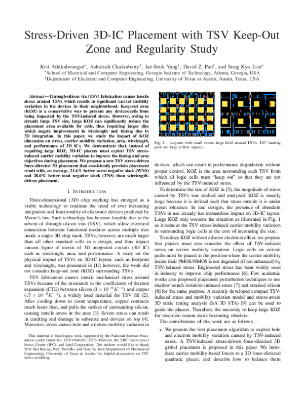
Fig. 1. Layouts with small versus large KOZ around TSVs. TSV landing
pads are large yellow squares.
devices, which can result in performance degradation without
proper control. KOZ is the area surrounding each TSV from
which all logic cells must “keep out” so that they are not
influenced by the TSV-induced stress.
To determine the size of KOZ in [5], the magnitude of stress
caused by TSVs was studied and analyzed. KOZ is usually
large because it is defined such that stress outside it is under
preset tolerance. In real designs, the presence of abundant
TSVs in use already has tremendous impact on 3D-IC layout.
Large KOZ only worsens the situation as illustrated in Fig. 1
as it reduces the TSV stress-induced carrier mobility variation
in surrounding logic cells at the cost of increasing die size.
To reduce KOZ without adverse electrical effect, we propose
that placers must also consider the effect of TSV-induced
stress on carrier mobility variation. Logic cells on critical
paths must be placed in the position where the carrier mobility
inside their PMOS/NMOS is not degraded (if not enhanced) by
TSV-induced stress. Engineered stress has been widely used
in industry to improve chip performance [6]. Few academic
works also proposed placement perturbation techniques to use
shallow trench isolation-induced stress [7] and strained silicon
[8] for the same purpose. A recently developed compact TSVinduced stress and mobility variation model and stress-aware
3D static timing analysis (SA 3D STA) [9] can be used to
guide the placers. Therefore, the necessity to keep large KOZ
for electrical reason starts becoming obsolete.
The contributions of this work are as follows:
•
This material is based upon work supported by the National Science Foundation under Grant No. CCF-0546382, CCF-0644316, the SRC Interconnect
Focus Center (IFC), and Intel Corporation. The authors would like to thank
Prof. Rui Huang, Prof. Paul Ho, and Gary Lu from Department of Mechanical
Engineering, University of Texas at Austin, for helpful discussions on TSV
stress modeling.
We present the first placement algorithm to exploit hole
and electron mobility variation caused by TSV-induced
stress. A TSV-induced stress-driven force-directed 3D
global placement is proposed in this paper. We introduce carrier mobility-based forces to a 3D force-directed
quadratic placer, and describe how to balance them
�against original placement forces.
We devise a way to integrate our placer to commercial
tools. The design flow enables us to perform, on GDSIIlevel 3D layouts, trial or detail route, parasitic extraction,
and finally SA 3D STA to find accurate critical paths and
critical nets/cells on them to guide the placer.
• Using the above mentioned design flow, we study the
impact of KOZ on stress, carrier mobility variation, area,
wirelength, and performance of 3D ICs. To the best of
our knowledge, this is the first work that studies TSVinduced stress and carrier mobility variation issues in the
context of KOZ and 3D-IC placement optimization.
The rest of this paper is organized as follows. First, the
compact TSV-induced stress and mobility variation models
and SA 3D STA [9] are reviewed in Section II. We describe
our TSV-induced stress-driven design flow in Section III. In
Section IV, we present our TSV-induced stress-driven forcedirected 3D global placement. Experimental results are shown
in Section V, followed by conclusions in Section VI.
•
II. P RELIMINARY W ORKS
A. Mobility Variation Modeling
To take TSV-induced stress into account for SA 3D STA,
an analytical model of TSV stress-induced carrier mobility
variation was proposed in [9]. Carrier mobility change depends
on not only applied stress, but also orientation between the
stress and a transistor channel. The effect from multiple TSVs
can be combined by using linear super-position. Total carrier
mobility variation ∆µ/µtotal is defined in [9] as
X ∆µ
X
∆µ
=
(θ) = −Π
(σi · α(θi )), (1)
µ total
µ
i∈TSVs
where Π is the tensor of piezo-resistive coefficients, σi is the
tensile stress caused by ith TSV, α(θi ) is the orientation factor
of ith TSV, and θi is the degree between the center of the ith
TSV and a point at which we want to obtain mobility variation.
B. Stress-Aware 3D Static Timing Analysis
Even though the layout of a cell is fixed, its timing characteristic can vary based on TSV stress-induced carrier mobility
variation. The SA 3D STA framework in [9] renames cells
in verilog netlist to reflect their carrier mobility variation. For
example, INVX1_N8_P8 is INVX1 with negative 8% hole
mobility change and positive 8% electron mobility change.
Cells with different mobility corners are characterized to make
carrier-mobility variation-aware library.
In the framework, a verilog netlist and a parasitic extraction
file (SPEF) for each die is prepared. A top level verilog netlist
instantiates the dies, and connects them using wires, which
correspond to TSVs. Finally, with a top level SPEF file for
the TSVs, PrimeTime can provide the SA 3D STA results.
III. TSV-I NDUCED S TRESS -D RIVEN P LACEMENT
O PTIMIZATION
In this section, we present an overview of our stressdriven timing optimization methodology. Basically, we use
#
!
"
"
#$"
!
!
(a) For regular TSV position
Fig. 2.
%
$
#
$
%
%
(b) For irregular TSV position
Design flow for TSV-induced stress-driven placement optimization.
the placement styles in [1] and develop our 3D placer for
stress-driven timing optimization as shown in Fig. 2. The
framework in [1] supports two different TSV placements,
namely, regular and irregular TSV position. In the case of
regular TSV position, TSVs are placed at regular grid-like
sites over the die area, and any net that needs to span multiple
dies must connect to these TSVs. In the case of irregular
TSV position, TSV and logic cell locations are determined
simultaneously. We modify global placement stage for stressdriven timing optimization because we have flexibility to move
cells to improve stress-aware timing. We do not perform any
kind of stress-driven timing optimization during routing stage
because TSV-induced stress mainly affects cell delay based on
cell location, which is not changed during routing.
For design with regular TSV position, called TSV-site in
[1], we start by partitioning logic cells into dies of a 3D
chip stack using a min-cut approach. Then, we estimate the
minimum number of signal TSVs required, and pre-place them
on the dies. Knowing location of pre-placed signal TSVs, we
calculate stress map on all dies for use during SA 3D STA.
Then, we perform TSV stress-driven global placement, which
is presented in Section IV, to obtain placement result. Note
that our placer calls SA 3D STA in order to obtain the sets
of nets and cells on critical paths to be optimized after every
predefined iteration. Then, we perform detail placement, and
assign TSVs to multiple-die nets in the 3D chip stack using
the same method as in [1]. After routing, we can evaluate
stress-aware performance from GDSII layout.
For design with irregular TSV position, called TSV coplacement in [1], the flow differs from that for design with
regular TSV position in a few ways. After partitioning, TSVs
are included into netlist as part of placement cells of multipledie nets using the same heuristic, called net splitting, as in
[1], and TSV assignment stage is not needed. Because TSV
position is changed in every placement iteration, stress map
needs to be regularly updated.
The presented design flow allows us to study the impact of
KOZ on stress, carrier mobility variation, area, wirelength, and
�performance of 3D ICs. The result of our study is analyzed,
and reported in detail in Section V.
IV. TSV S TRESS -D RIVEN G LOBAL P LACEMENT
In this section, we describe our TSV stress-driven global
placement algorithm. It is based on a forced-directed quadratic
placement [10], which was extended to support 3D-IC design
in [1]. We introduce carrier mobility-based forces, and describe
how to balance them against original placement forces in both
works. We also discuss convergence of the algorithm when
placing design with many TSVs with large KOZ.
(a) Hole mobility
Fig. 3.
(b) Electron mobility
Carrier mobility variation surface surrounding TSVs.
A. Overview of 3D Force-Directed Quadratic Placement
Placement result in a quadratic placement [10] is computed
by minimizing the quadratic wirelength function Γ defined as
Γ = Γx +Γy , where Γx and Γy are wirelength along x- and yaxis. We can minimize Γx and Γy separately because they are
independent. For brevity, only description for x-dimension is
given in this paper because it similarly applies to y-dimension.
Here, Γx can be written in a matrix form as
1
(2)
Γx = xT Cx x + xT dx + constant,
2
where vector x represents the x-position of cells to be placed,
matrix Cx represents the connection among the cells along
x-axis, and vector dx represents the connection to fixed pins
along x-axis. Treating Γx as the energy of a spring system,
we can view its derivative as net force fxnet defined as
fxnet = ∇x Γx = Cx x + dx ,
(3)
where ∇x is vector differential operator. The minimum Γx is
found when fxnet is zero, but cells can overlap in few small
areas. Density-based force fxden spreads cells away to reduce
cell overlap, and is defined as
fxden = C̊dx (x − x̊d ),
(4)
where vector x̊d represents the x-position of target points
to which cells are connected by density-based springs, and
d
diagonal matrix C̊dx collects spring constants ẘx,i
of densityhold
based spring connected to cell i. Hold force fx
decouples
successive placement iterations by canceling out net force that
pulls cells back to the initial placement, and is defined as
fxhold = −(Cx x′ + dx ),
(5)
′
where vector x represents the x-position of cells from last
iteration. The placement result for each placement iteration
can be obtained by setting total force fx to zero, or solve
fx = fxnet + fxden + fxhold = 0.
(6)
B. Carrier Mobility-Based Forces
To consider the effect of TSV stress-induced carrier mobility
variation during global placement, we need to introduce two
additional forces, one for hole mobility variation fxmobil,h and
another for electron mobility variation fxmobil,e , into (6).
Here, fxmobil,h and fxmobil,e can be separately defined because
they aim to optimize delay of different devices, e.g. PMOS and
NMOS. For brevity, only description related to hole mobility
is given in this paper because it similarly applies to electron
mobility. The force can be represented by hole mobility-based
springs connected to cells, and defined as
m,h
fxmobil,h = C̊m,h
),
x (x − x̊
[x̊m,h
1
(7)
T
x̊m,h
N ]
where vector x̊m,h =
···
represents the xposition of target points to which N cells are connected
by hole mobility-based springs, and diagonal matrix C̊m,h
x
m,h
collects spring constants ẘx,i
of hole mobility-based spring
connected to cell i.
Hole mobility-based target point x̊m,h
on die d is defined
i
as
¯
¯
∂
m,h
Φ
(x,
y)
¯
m,h
m,h
′
x̊i = xi + li · ∂x m,h
,
(8)
¯
k∇Φ (x, y)k ¯ ′ ′
(xi ,yi ),z=d
where vector x′ = [x′1 · · · x′N ]T represents the x-position
of N cells from last iteration, Φm,h (x, y) = ∆µ
µ total (x, y) is
hole mobility variation surface charted by using the model
described in Section II, ∇Φm,h (x, y) is its gradient, and lim,h
is a length along the gradient direction of the surface. The
gradient is added to current position in this equation because
we want to move cell in the direction of hole mobility increase.
The carrier mobility variation surfaces are shown in Fig. 3.
The green area in the figures indicates carrier mobility enhancement caused by TSV-induced stress, and the red area
indicates degradation. Unlike placement density, carrier mobility variation surface is smooth (except at TSV edge because
mobility variation is not defined inside TSVs). Therefore, we
can determine the direction of target points to which cells are
connected by mobility-based springs from its gradient directly.
1) Balancing Forces: The newly introduced fxmobil,h needs
to be balanced against fxden and fxnet (no need to balance
against fxhold ). The force-directed quadratic placement in [10]
already has a mechanism to balance fxden against fxnet so
that the speed of cell spreading is regulated across placement
iterations. We can use the same mechanism, and, therefore,
balance fxmobil,h against only fxden . The parameters that need
adjustment are the length along the gradient direction of hole
mobility variation surface lim,h and hole mobility-based spring
m,h
.
constant ẘx,i
We choose lim,h so that hole mobility at the target point
is higher than that at the current cell position. We start with
�TABLE I
B ENCHMARK CIRCUITS .
Circuit
ckt1
ckt2
ckt3
ckt4
ckt5
(a) On hole mobility variation surface
Fig. 4.
(b) On electron mobility variation
surface
All forces applied to a cell.
the length of 1/8 × average cell size, and increase it to 1/4,
1/2, and 1 × average cell size while hole mobility increases.
We stop at the length of average cell size so that we do not
increase wirelength too much. If hole mobility at even 1/8 ×
average cell size is lower than that at the current cell position,
we do not apply hole mobility-based force to that cell at all
in that iteration.
Compared to density-based gradient, which directly defines
the length to density-based target point in (4), lim,h is relatively
constant. Density-based gradient is extremely high in early
placement iterations because of cell overlap, and decreases to
almost zero as overlap is resolved in late iterations [10]. By
limiting lim,h to average cell size, we naturally balance it to
the length to density-based target point. The length to densitybased target point dominates during early iterations, and the
effect of lim,h becomes pronounced when the length to densitybased target point drops below lim,h during late iterations.
During global placement, we perform SA 3D STA periodically. The results from SA 3D STA include the set of
cells whose rise- and/or fall-time slack is negative. Then,
m,h
we balance hole mobility-based spring constant ẘx,i
against
d
density-based spring constant ẘx,i
of diagonal matrix C̊dx in
(4) by defining it as
m,h
d
ẘx,i
= cih,j × ẘx,i
,
(9)
where ch,j
is rise-time criticality of cell i after j th SA 3D
i
STA, and defined as
( h,j−1
j
h,j
(ci
+ sh,j
i /Smin )/2 if i ∈ Cc
h,j
(10)
ci =
ch,j−1
/2
otherwise,
i
j
where sh,j
is rise-time slack of cell i, Smin
is minimum timing
i
h,j
slack of the design, and Cc is the set of cells whose rise-time
j
slack is negative and less than 90% of Smin
. In other words,
we determine cell rise-time criticality based on its history and
current rise-time slack. Therefore, the effect of hole mobilitybased spring is pronounced on a cell whose rise-time is highly
critical, and needs hole mobility enhancement.
2) New Total Force: An illustration of all forces applied
to a cell is shown in Fig. 4. In the figure, f net tries to hold
the yellow cells of a net together, but f hold tries to nullify
its effect, allowing cells to be moved based on other forces.
Because of high cell density on top of right yellow cell, f den
#Gates
20K
33K
50K
80K
119K
#Nets
20K
33K
51K
80K
119K
#TSVs
634
3, 554
5, 352
2, 846
5, 341
Profile
Microprocessor
Arithmetic Unit
Connection Bus
Network Controller
Data Encryption
tries to move the cell down. If the cell is rise-time critical,
f mobil,h tries to move the cell toward top right, away from the
TSV, where hole mobility degradation decreases as shown in
Fig. 4(a). If the cell is, however, fall-time critical, f mobil,e tries
to move the cell left, toward the TSV, where electron mobility
increases as shown in Fig. 4(b). In the case that a cell is both
rise- and fall-time critical, the result depends on which timing
is more critical.
With the newly introduced hole mobility-based force
fxmobil,h and electron mobility-based force fxmobil,e , the total
force becomes
fx = fxnet + fxhold + fxden + fxmobil,h + fxmobil,e .
(11)
By setting fx = 0 and substituting equations, the new result
for each placement iteration can be obtained by solving
m,h m,h
d d
+ C̊m,e
(Cx + C̊dx + C̊m,h
x )∆x = −C̊x Φ + C̊x Φ
x
m,e
+ C̊m,e
(12)
x Φ
for ∆x, where vector ∆x = x − x′ indicates how far cells
should be moved, Φd is the vector collecting density-based
gradients, and Φm,h and Φm,e are the vectors collecting lim,h ·
∂
∂
m,h
/k∇Φm,h k and lim,e · ∂x
Φm,e /k∇Φm,e k from (8).
∂x Φ
C. Convergence of Stress-Driven Global Placement
We found that introducing f mobil,h and f mobil,e to 3D forcedirected quadratic placement without proper monitoring may
cause problem to its convergence. During the early iterations
of designs with irregular TSV position, highly overlapping
TSVs in a region result in extremely high mobility variation,
which can misguide the placer. Because TSVs are also moved
in every placement iteration as well to resolve their overlap,
carrier mobility surfaces change. Critical cells are pulled by
overlapping TSVs, worsening wirelength, until the overlap is
finally resolved, and realize that the mobility improvement
already vanishes. To prevent this problem, we put an upperbound limit on mobility variation from (1).
Another problem arises when a cell is moved over the top of
a TSV or its KOZ during placement iterations. When a cell is
inside a TSV, (1) is not defined. Also the mobility variation is
not valid when a cell is inside KOZ because the cell is moved
out of KOZ during legalization. We do not apply f mobil,h and
f mobil,e to the cell under these cases to prevent the placer from
being misguided.
V. E XPERIMENTAL R ESULTS
We use IWLS 2005 benchmarks [11] and several industrial
circuits as listed in Table I. We use 45nm technology for
�TABLE II
I MPACT OF KOZ
TSV
Cell
2-row
3-row
4-row
5-row
6-row
7-row
ON CARRIER MOBILITY VARIATION FOR CKT 5.
Mobility Variation (%)
Regular TSV Position
Irregular TSV Position
Hole
Electron
Hole
Electron
-4.56 – 2.81
0.33 – 3.62
-8.76 – 4.74
0.02 – 7.47
-4.05 – 2.45
0.30 – 2.35
-6.04 – 2.55
0.02 – 4.10
-2.07 – 1.51
0.26 – 1.37
-2.87 – 1.75
0.02 – 2.17
-1.55 – 0.93
0.18 – 0.89
-2.30 – 1.26
0.02 – 1.32
-1.01 – 0.70
0.13 – 0.64
-1.33 – 0.70
0.02 – 0.85
-0.90 – 0.53
0.07 – 0.40
-1.15 – 0.61
0.02 – 0.62
TABLE III
I MPACT OF KOZ ON AREA AND WIRELENGTH FOR CKT 5.
TSV
Cell
2-row
3-row
4-row
5-row
6-row
7-row
Footprint
(mm2 )
0.176
0.250
0.360
0.504
0.672
0.884
(1.00)
(1.42)
(2.04)
(2.86)
(3.81)
(5.01)
TSV Cell Area
(mm2 )
0.130
0.293
0.521
0.815
1.173
1.597
(18.47%)
(29.33%)
(36.21%)
(40.40%)
(43.61%)
(45.17%)
Wirelength (m)
Regular
Irregular
TSV Position TSV Position
3.415 (1.00)
2.970 (1.00)
3.970 (1.16)
3.475 (1.17)
4.726 (1.38)
4.196 (1.41)
5.526 (1.62)
4.654 (1.57)
6.331 (1.85)
5.328 (1.79)
7.179 (2.10)
6.036 (2.03)
KOZ increases, and starts becoming negligible (1% or less)
when TSV cell size reaches 6-row. We also observe that
mobility variation in design with irregular TSV position is
larger than that in design with regular TSV position. TSV
cells in design with irregular TSV position can be crowded in
some area, causing high stress and mobility variation.
B. Impact of KOZ on area and wirelength
The main purpose of KOZ is to prevent cells from being
placed so close to TSV that they experience carrier mobility
variation. The side effect of enforcing large KOZ to have
predictable device performance is shown in Table III. The
footprint area of the chip stack for ckt5 increases almost 4×
if TSV cell size is 6-row. The increased area is primarily
consumed by TSV cells. In an extreme case, almost half of
silicon area is consumed by TSV cells when TSV cell size
is 7-row. Increasing footprint area inevitably results in 2×
wirelength increase due to large KOZ choice.
C. Impact of KOZ on stress-aware timing
(a) With regular TSV position on
hole mobility variation surface
(b) With regular TSV position on
electron mobility variation surface
(c) With irregular TSV position on
hole mobility variation surface
(d) With irregular TSV position on
electron mobility variation surface
Fig. 5. Zoom-up snapshots of stress-driven placement results for ckt3 using
2-row TSV cells.
our experiments with TSV size of 3µm. The TSV parasitic
capacitance and resistance are 50f F and 0.2Ω, respectively.
We expand KOZ around TSVs to make TSV cells (= TSV +
KOZ) fit inside 2–7 standard-cell rows (1 standard-cell row =
2.47µm). We base all our experiments on 4-die chip stack with
constant cell area density. We use min-cut partitioner, and set
the target clock period to the value reported after synthesis.
All reported timing results come from SA 3D STA.
A. Impact of KOZ on carrier mobility variation
In this experiment, we increase TSV cell size from 2-row
to 7-row while observing carrier mobility variation caused by
TSV-induced stress. The results are shown in Table II. The
result indicates that carrier mobility variation decreases as
We run SA 3D STA after obtaining placement results from
wirelength-driven, timing-driven, and stress-driven placers.
The results are shown in Table IV. First, we observe that,
under TSV-induced stress, the timing results from timingdriven placement can be unpredictable, and worse than the
results from even wirelength-driven placement in many cases.
Traditional timing-driven placer is oblivious to the change
in carrier mobility of devices, and only tries to reduce the
capacitive load on timing critical cells. Second, we observe
that our stress-driven placer outperforms timing-driven placer
consistently. The improvements over wirelength-driven placement on worst negative slack (WNS) and total negative slack
(TNS) are up to 39% and 42% respectively. Third, we also
observe that, using 2-row TSV cells, our stress-driven placer
provides better result for design with irregular TSV position
than the result for design with regular TSV position. Design
with irregular TSV position has shorter wirelength and higher
carrier mobility variation which our placement algorithm can
intelligently exploit. Finally, we observe that, as TSV cell
size increases, the benefit from our stress-driven placement
decreases. Large KOZ leaves not much mobility variation for
our stress-driven placement to exploit.
D. Stress-driven placement results
We obtain placement results from our stress-driven placer.
The snapshots of ckt3 are shown in Fig. 5. In the figures,
gray band surrounding TSVs is KOZ. Logic cells in magenta
are hole mobility critical cells. Their timing arcs are rising
on the critical paths. Our placer positions them (if possible)
in green area of Fig. 5(a) where they receive hole mobility
enhancement, or, at least, in black area where they do not
experience hole mobility degradation. On the other hand,
logic cells in sky blue are electron mobility critical cells.
Their timing arcs are falling on the critical paths. Our placer
positions them (if possible) in bright green area of Fig. 5(b)
where they receive higher electron mobility enhancement.
�TABLE IV
I MPACT OF KOZ
TSV
Cell
2-row
3-row
4-row
5-row
6-row
7-row
Regular TSV Position
Wirelength-Driven
Timing-Driven
WNS (ps) TNS (ps)
WNS
TNS
(=100%)
(=100%)
(%)
(%)
-92.72
-143
113.66
126.57
-96.62
-156
70.14
65.38
-102.86
-170
85.06
82.94
-99.28
-157
88.43
87.90
-88.45
-139
99.27
99.28
-88.55
-139
99.02
99.28
ON STRESS - AWARE TIMING FOR CKT 5.
Stress-Driven
WNS
TNS
(%)
(%)
77.01
69.93
70.60
62.82
78.20
74.71
88.48
87.90
99.31
99.28
99.09
99.28
Irregular TSV Position
Wirelength-Driven
Timing-Driven
WNS (ps) TNS (ps)
WNS
TNS
(=100%)
(=100%)
(%)
(%)
-79.26
-120
127.26
143.33
-77.89
-118
133.11
147.46
-85.42
-134
111.53
114.18
-88.32
-139
100.83
100.72
-88.33
-139
99.43
99.28
-88.28
-139
99.63
99.28
Stress-Driven
WNS
TNS
(%)
(%)
60.62
57.50
94.12
92.37
92.95
90.30
99.91
99.28
99.54
99.28
99.43
99.28
TABLE V
T IMING COMPARISON FOR REGULAR AND IRREGULAR TSV POSITION WITH 2- ROW TSV S .
Circuit
ckt1
ckt2
ckt3
ckt4
ckt5
AVE (%)
Regular TSV Position
Wirelength-Driven
Timing-Driven
WNS
TNS
WNS
TNS
(ps)
(ps)
(ps)
(ps)
-163.50
-1,167
-156.67
-1,034
-159.35
-5,104
-180.86
-6,076
-79.35
-605
-65.85
-428
-55.39
-131
-49.25
-106
-92.72
-143
-105.39
-181
100.00
100.00
98.98
97.18
Stress-Driven
WNS
TNS
(ps)
(ps)
-156.39
-1,034
-129.35
-4,105
-53.72
-321
-38.01
-72
-71.40
-100
78.03
69.40
The results from different placement algorithms using 2row TSV cells are shown in Table V. On average, timingdriven placer does not provide performance improvement over
wirelength-driven placer when evaluated by SA 3D STA. The
cells on critical paths may be placed in location that carrier
mobility is degraded by TSV-induced stress. On the other
hand, stress-driven placer consistently provides better performance than the other placers. On average, the performance
improvement over wirelength-driven placement on WNS and
TNS are 21.6% and 28.0% respectively. We observe again that
the results for design with irregular TSV position are better
than those for design with regular TSV position in all cases.
VI. C ONCLUSIONS
In this paper, we analyzed the impact of choice of KOZ
dimension around TSVs on the mechanical stress, carrier
mobility variation, area, wirelength, and performance of 3D
ICs. Use of large KOZs was observed to practically nullify
the impact of TSV-induced stress on carrier mobility but at
the cost of almost 4× increase in chip stack footprint area
and 2× increase in wirelength. In addition, we observed that,
to regain footprint area by reducing KOZ dimension, 3DIC placers must be TSV stress-aware to extract best circuit
performance by exploiting the TSV stress-dependent mobility
variation instead of avoiding it. Lastly, we proposed the first
TSV-induced stress-driven force-directed 3D global placer by
adding new carrier (hole and electron) mobility-based forces to
traditional force-directed placement. Compared to wirelengthdriven placement, our placer results in superior placement with
average reductions of WNS by 21.6% and TNS by 28.0%.
R EFERENCES
[1] D. H. Kim, K. Athikulwongse, and S. K. Lim, “A study of throughsilicon-via impact on the 3D stacked IC layout,” in Proc. IEEE Int.
[2]
[3]
[4]
[5]
[6]
[7]
[8]
[9]
[10]
[11]
Wirelength-Driven
WNS
TNS
(ps)
(ps)
-157.04
-1,063
-127.28
-4,005
-73.40
-482
-50.38
-109
-79.26
-120
100.00
100.00
Irregular TSV Position
Timing-Driven
WNS
TNS
(ps)
(ps)
-161.21
-1,107
-134.70
-4,327
-56.65
-348
-40.75
-80
-100.87
-172
98.76
100.22
Stress-Driven
WNS
TNS
(ps)
(ps)
-155.15
-1,004
-120.45
-3,888
-51.88
-307
-34.95
-66
-48.05
-69
78.82
74.65
Conf. Computer-Aided Design, San Jose, CA, Nov. 2–5 2009, pp. 674–
680.
T. Dao, D. H. Triyoso, M. Petras, and M. Canonico, “Through silicon via
stress characterization,” in Proc. IEEE Int. Conf. on Integrated Circuit
Design and Technology, Austin, TX, May 18–20 2009, pp. 39–41.
K. H. Lu et al., “Thermo-mechanical reliability of 3-D ICs containing
through silicon vias,” in IEEE Electronic Components and Technology
Conf., San Diego, CA, May 26–29 2009, pp. 630–634.
C. S. Selvanayagam et al., “Nonlinear thermal stress/strain analyses of
copper filled TSV (through silicon via) and their flip-chip microbumps,”
in IEEE Electronic Components and Technology Conf., Lake Buena
Vista, FL, May 27–30 2008, pp. 1073–1081.
C. Okoro et al., “Analysis of the induced stresses in silicon during
thermcompression Cu-Cu bonding of Cu-through-vias in 3D-SIC architecture,” in IEEE Electronic Components and Technology Conf., Reno,
NV, May 29–June 1 2007, pp. 249–255.
S. E. Thompson et al., “A 90-nm logic technology featuring strainedsilicon,” IEEE Trans. on Electron Devices, vol. 51, no. 11, pp. 1790–
1797, Nov. 2004.
A. B. Kahng, P. Sharma, and R. O. Topaloglu, “Exploiting STI stress
for performance,” in Proc. IEEE Int. Conf. Computer-Aided Design, San
Jose, CA, Nov. 5–8 2007, pp. 83–90.
A. Chakraborty, S. X. Shi, and D. Z. Pan, “Layout level timing
optimization by leveraging active area dependent mobility of strainedsilicon devices,” in Proc. Design, Automation and Test in Europe,
Munich, Germany, Mar. 10–14 2008, pp. 849–855.
J.-S. Yang, K. Athikulwongse, Y.-J. Lee, S. K. Lim, and D. Z. Pan,
“TSV stress aware timing analysis with applications to 3D-IC layout
optimization,” in Proc. ACM Design Automation Conf., Anaheim, CA,
June 13–18 2010, pp. 803–806.
P. Spindler, U. Schlichtmann, and F. M. Johannes, “Kraftwerk2–A
fast force-directed quadratic placement approach using an accurate net
model,” IEEE Trans. Computer-Aided Design of Integrated Circuits and
Systems, vol. 27, no. 8, pp. 1398–1411, Aug. 2008.
IWLS. (2005, June) IWLS 2005 benchmarks. [Online]. Available:
http://www.iwls.org/iwls2005/benchmarks.html
�
 David Pan