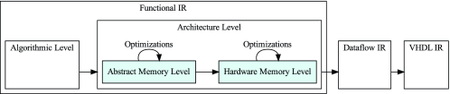
4.4.1 Abstract Memory Level.
Type. The type constructor RamArrayT\( (T^{BasicDataT}, N^{NatT}, ML^{MemLocT}) \) (short-form notation \( \hspace{3.00003pt}\rotatebox [origin=c]{90}{RAM}\hspace{1.00006pt} [T]_{N}^{ML} \)) represents a ramarray of \( N \) elements of type \( T \), which can only be accessed one at a time, however, random-order access is possible. Shir features a flat memory model and forbids nesting of RamArrayT. Multi-dimensional data is stored in memory by joining (i.e., flattening) the data before writing to memory and then splitting it after reading. The ramarray’s MemLocT indicates whether host Random Access Memory (RAM) HostRamT or on-chip block RAM BlockRamT is used to hold the data. This type also contains an identifier to distinguish between multiple block RAM instances.
Primitives. Figure
8 shows the Abstract Memory Level primitives.
MemAlloc allocates memory space for
\( N \) elements of type
\( T \) and returns a ramarray. A
MemLocT is required, to identify the memory used. Given a ramarray, the
Read primitive returns an element at the specified address of type
\( A \). The bit-width
\( b \) of the address depends on the ramarray’s length, with
\( b = \lceil \log _2 N \rceil \).
The Write primitive enables the reverse operation: writing a new element at a given position in a ramarray. Similar to the concept of monads in functional programming, this primitive returns the updated ramarray. However, the later generated hardware implementation updates the data in-place. Thus, an interesting pattern of code is enabled: By wrapping Write into a ReduceStm, an entire stream can be buffered in a ramarray. In practice, this is beneficial when the ramarray resides on-chip and the stream is read multiple times. The following code illustrates this important use-case, where the stream inputData is stored in a ramarray, and then read again:
4.4.2 Hardware Memory Level.
Types. At the Hardware Memory Level, the ramarray types disappear, because memory is represented as functions. This corresponds to the hardware paradigm that interaction with memory is performed through functional units. Depending on the type of memory involved, on-chip versus off-chip, the function is either synchronous (data is returned immediately) or asynchronous (requested data is returned later and not in order).
To capture this in the type system, the IR is expanded with a new function type. Its type constructor is ArchFunT\( (inT^{ValueT}, outT^{ValueT}, c^{CommT}) \). In short-form notation, we use \( \;inT \xrightarrow {s} outT\; \) for synchronous communication (where \( c \) is SyncT) and \( \;inT \xrightarrow {a} outT\; \) f or asynchronous communication (\( c \) is AsyncT).
Primitives for Synchronous Block RAM. At this level, there is no abstract
MemAlloc primitive but a more specialized
BlockRam primitive, shown in Figure
9, to model synchronous on-chip RAM as functions. When called, this primitive returns a function that accepts a piece of data, an address and a write-enable flag which determines whether we want to read or write. This functional design is in line with its resulting hardware implementation.
Additionally, memory controllers are introduced, which extract only a certain capability of the memory interface. The ReadSyncMemCtrl primitive takes a BlockRam and provides an interface which only allows us to read data. The write enable flag is not accessible any longer from the outside and is fixed to false internally. The WriteSyncMemCtrl extracts a write interface, setting the write enable to true internally. The provided interface from WriteSyncMemCtrl, takes a value and an address and returns the same value after writing.
ReadSync uses the ReadSyncMemCtrl to read a value at a certain address from the block RAM memory, which is behind the memory controller. This primitive calculates the actual requested address by adding the given base address and given offset, both subtypes of integer. The WriteSync primitive works in a similar way, but instead takes a tuple of data and offset as input.
Primitives for Asynchronous Host RAM. The notion of host RAM is always present in the system and there is no need to allocate it. Therefore, there is no counterpart primitive to the BlockRam. The Hardware Memory Level provides memory controllers for both reading and writing asynchronous memory. During hardware generation, these controllers are connected to the DMA interface of the FPGA which talks to the host RAM via the Peripheral Component Interconnect Express (PCIe) bus.
Each asynchronous memory access must specify a unique request id (\( R \) in the type) to link a response to the requested read or write operation. ReadHostMemCtrl provides an asynchronous function, which takes a tuple of address and request id and returns a tuple of data and request id. The asynchronous function of the WriteHostMemCtrl takes a tuple of address, data, and request id and just returns the same request id, when the data has been written to the address in host RAM.
The host memory controller’s signature for reading and writing depends on the FPGA DMA interface specifications. The Intel Arria 10 in our system transfers cache lines of 512 bits via DMA. Smaller pieces of data must be packed and possibly padded with zeros to fill an entire line. For this case, Shir offers a smart converter that creates a combination of split, join and other reshaping primitives to convert cache lines into any desired type of data with arbitrary precision and back. For 7-bit values each cache line contains \( \lfloor 512 / 7 \rfloor = 73 \) elements with (512 mod 7) = 1 padding bit.
The primitives for reading and writing are refined to enable concurrent memory requests. They take the corresponding memory controller and a base address as input. In addition, ReadAsync consumes a stream of addresses, while WriteAsync consumes a stream of tuples of address and data. Without waiting for the responses of previous requests (non-blocking), these asynchronous primitives send new requests to memory one by one, as soon as a new value from the input stream arrives. Thus, throughput between the host and the FPGA is maximized using multiple in-flight requests. The input stream’s length of ReadAsync and WriteAsync determines the maximum number of possible parallel requests. Once the requested data is loaded, the host sends a response with the payload attached. WriteAsync returns the base address, when all the write operations to this memory region are completed and confirmed by the memory controller.
While the IR design looks complicated on the surface, it directly maps to hardware concepts and provides great flexibility in terms of expressible hardware designs.