INTL JOURNAL OF ELECTRONICS AND TELECOMMUNICATIONS, 2012, VOL. 58, NO. 3, PP. 225–232
Manuscript received January 28, 2012; revised March, 2012.
DOI: 10.2478/v10177-012-0031-5
A Precise and High Speed Charge-Pump PLL
Model Based on SystemC/SystemC-AMS
Kezheng Ma, Rene van Leuken, Maja Vidojkovic, Jac Romme,
Simonetta Rampu, Hans Pflug, Li Huang, and Guido Dolmans
Abstract—The Phase Locked Loop (PLL) has become an
important part of electrical systems. When designing a PLL, an
efficient and reliable simulation platform for system evaluation
is needed. However, the closed loop simulation of a PLL is
time consuming. To address this problem, in this paper, a new
PLL model containing both digital and analog parts based
on SystemC/SystemC-AMS (BETA version) is presented. Many
imperfections such as Voltage Control Oscillator (VCO) noise
or reference jitter are included in this model. By comparing
with the Matlab model, the SystemC/SystemC-AMS model can
dramatically reduce simulation time. Also, by comparing with
Analog Devices ADI SimPLL simulation results, Cadence simulation results and real measurement results, the accuracy of the
SystemC/SystemC-AMS model is demonstrated. The paper shows
the feasibility of a unified design environment for mixed-signal
modelling based on SystemC/SystemC-AMS in order to reduce
the cost and design time of electrical systems.
Keywords—SystemC/SystemC-AMS, Phase Locked Loop
(PLL), radio frequency, mixed-signal modeling, hardware
description language.
I. I NTRODUCTION
P
HASE Locked Loops (PLL) have become an important
part of electrical systems. It is widely used in radios,
computers, telecommunications, and other electronic applications. However, when designing a PLL, one of the main
problems is that the closed loop simulation of a PLL is very
time consuming, especially at transistor level. For example,
a fine frequency resolution required in noise simulation often
leads to an over 24-hour simulation time [1]. Therefore, to
examine the closed loop behavior, a fast and precise model is
highly desirable.
Many efforts have been spent to address this problem, such
as in [1] and [2] where Verilog-AMS models are presented.
However, these models have their limitations in terms of
simulation performance. For instance, in [1], the high frequency output of the Voltage Control Oscillator (VCO) is
not generated in order to reduce simulation time. But in this
way, it is impossible to insert the PLL into a radio system
model for further testing. In [2], although the VCO output
is generated, performing a 60us transient analysis requires
15 minutes. Consequently, the simulation time will be over
4 hours if a transient analysis over 1000us (for noise analysis)
is needed.
Rene van Leuken is with Delft University of Technology,
Mekelweg 4, 2628 CD Delft, Netherlands. All other authors are
with Holst Centre, HTC 31, 5656 AE, Eindhoven, Netherlands
(e-mails:
mkz1986@hotmail.com;
t.g.r.m.vanleuken@tudelft.nl;
simonetta.rampu@gmail.com; {Maja.Vidojkovic; Jac.Romme; Hans.Pflug;
Li.Huang; Guido.Dolmans}@imec-nl.nl).
To further improve simulation time while still keeping
good accuracy, a new mixed-signal PLL model based on
SystemC/SystemC-AMS (BETA version) is proposed in this
paper. Unlike many other high center frequency models, the
model in this paper does not combine the divider and the VCO.
Consequently, the high frequency VCO output is available,
which enables designers to insert the PLL into a radio system
model to evaluate the overall system performance. In the
past, we published one paper on SystemC/SystemC-AMS PLL
model [3]. However, this model only has basic functionality
and includes limited practical imperfections. To develop a
more realistic model for system design, many imperfections
are included in the model proposed in this paper, e.g. VCO
noise, PLL Dead Zone, Phase Frequency Detector (PFD) reset
delay, Charge Pump (CP) current mismatch, CP leakage current, the reference jitter and Delay difference between the CP
control signal. The simulation results of the proposed model
are compared with the simulation (measurement) results of a
Matlab model, Analog Devices ADI SimPLL tool, Cadence,
and real chip implementation. The comparison results verify
that the SystemC/SystemC-AMS model is precise with fast
simulation time.
The paper is organized as follows. The SystemC/SystemCAMS language is briefly introduced in section II. The structure
of the model is discussed in section III. The behavioral
modeling of each PLL block is shown in section IV. Our
proposed model is verified in section V. Finally, conclusions
are given in section VI.
II. I NTRODUCTION
TO
S YSTEM C/S YSTEM C-AMS
SystemC/SystemC-AMS is an effective system-level simulation and modeling language. It has many advantages. First of
all, it is a C++ based language which ensures fast calculation
speed. Moreover, it can take advantage of C++ power by
using a large number of existing C++ functions and libraries.
Secondly, SystemC/SystemC-AMS support hardware and software co-design which is very important to the design of a very
complex system. Last but not least, SystemC/SystemC-AMS
is an open source language, which requires no license fee for
the usage.
A. SystemC
SystemC is a C++ based language. It adds a class library to
C++ which enables it to describe hardware. SystemC is able to
describe the concepts that are familiar to hardware designers,
such as signals, modules and ports.
Unauthenticated
Download Date | 10/9/16 10:56 PM
�226
K. MA, R. VAN LEUKEN, M. VIDOJKOVIC, J. ROMME, S. RAMPU, H. PFLUG, L. HUANG, G. DOLMANS
SystemC does not add any new syntax to C++. Instead, it
only adds a library class to describe the concepts in hardware
design. Thus, SystemC is essentially C++. For this reason, the
designers can conveniently use the standard C++ developing
tools to simulate, debug and execute all kinds of algorithms
and structures. More importantly, with SystemC, a hardware
model could be made in system level as well as Register
Transfer Level (RTL). We can first make a system level model
to simulate and optimize the design quickly. Then we can
transfer the design to RTL level for synthesis.
The language structure of SystemC is shown below. In the
first part, the input and output ports are defined. The second
part illustrates the methods used to describe the function of
this module and in the third part, the constructor of the module
is presented.
SC_MODULE (example){
sc_in<double> input1, input2;
sc_in<bool> input3, input4;
sc_out<double> output1, output2;
Fig. 1.
A TDF model with 3 TDF modules [4].
Fig. 2.
A LSF model with 4 LSF modules [4].
Fig. 3.
A basic ELN model [4].
void prc_example();
SC_CTOR(example){
SC_THREAD(prc_example);
}
};
SystemC is very suitable for modeling the digital circuits.
However, its main limitation is the disability of simulating
analog or mixed signals. For this reason, SystemC-AMS is
introduced as a complement to deal with this inconvenience.
B. SystemC-AMS
In order to simulate the analog circuits, AMS extensions
based on SystemC are introduced. The SystemC-AMS extensions are built on top of the SystemC language standard
IEEE 1666-2005. They define additional language constructs,
which introduce new execution semantics and system-level
modelling methodologies to design and verify mixed-signal
systems [4]. They can be further divided into three models
– Timed Data Flow model (TDF), Linear Signal Flow model
(LSF), Electrical Linear Networks model (ELN).
1) TDF model: As shown in Fig. 1, the TDF model is a
discrete-time model. It considers the data as sampled signals
in time. Each TDF model is composed of a number of TDF
modules which are connected with TDF signals and TDF
ports. In each module, C++ methods are used to describe a
function of the module.
2) LSF model: The LSF model is a continuous-time module. This model provides a finite number of LSF modules
to implement calculation such as addition, subtraction and
multiplication. The users are not allowed to define their own
blocks. In other words, LSF model can only be composed
with the provided modules. LSF signals are used to connect
the modules. In this way, the equation system will be formed
to relate the inputs and outputs. Fig. 2 shows a basic LSF
model.
3) ELN model: As shown in Fig. 3, in ELN model, a set
of electrical primitives such as sources (voltage or current),
linear lumped elements (resistors, capacitors, inductors) are
provided. Designers model the circuit by connecting these
primitives with electrical nodes. The system will follow the
Kirchhoff’s current and voltage laws. ELN terminals are used
to communicate with other models.
C. Simulation Flow
The simulation flow is shown in Fig. 4. The digital parts of
the system are modeled with SystemC while the analog parts
are modeled with SystemC-AMS. After transient simulations,
the generated data will be loaded into Matlab to perform
frequency analysis.
Unauthenticated
Download Date | 10/9/16 10:56 PM
�A PRECISE AND HIGH SPEED CHARGE-PUMP PLL MODEL BASED ON SYSTEMC/SYSTEMC-AMS
227
A. Reference Clock Block
The reference clock block is used to generate the reference
clock of the PLL. It is modelled with SystemC because it is a
pure digital block. Part of the source code of reference block is
shown below. It works as follows: the period of the reference
clock is T, then every T/2, the output will reverse its value. The
function gauss() is used to generate a gauss random number
with 0 mean and variance of jitter which is used to model the
reference jitter.
SC_MODULE (refrence){
sc_out<bool> out;
Fig. 4.
void prc_refrence();
SystemC/SystemC-AMS model design flow.
SC_CTOR(refrence){
SC_THREAD(prc_refrence);
}
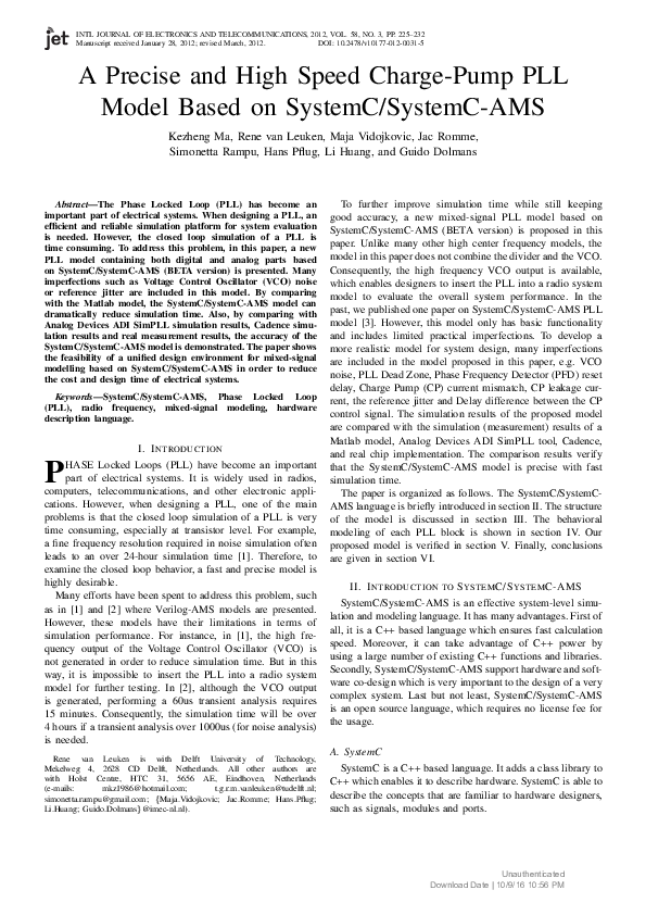
III. T HE PLL M ODEL S TRUCTURE
In radio transmitters, an integer N-PLL is used to synthesize
new frequencies which are multiples of a reference frequency,
with the same stability as the reference frequency. The structure of the integer PLL modeled in this paper is shown in
Fig. 5, in which the reference clock block, phase/frequency detector (PFD) block, divider block, rfdelay block are modelled
with SystemC and other blocks are modelled with SystemCAMS.
};
void refrence::prc_refrence(){
out=0;
while(1)
{
out=!out;
wait(T/2+gauss(jitter),SC_US);
}
}
B. The PFD Block
Fig. 5.
Structure of the PLL model.
As shown in the figure, the model is composed of eleven
blocks, a reference clock block, a phase/frequency detector
block, two rfdelay blocks, an inverter block, a charge pump
block, a control m block, a loop filter (LF) block, a voltage
control oscillator block, a converter block and a divider block.
The reference clock block is used to generate reference signal,
the PFD block is used to detect the phase/frequency difference
between the reference signal and the divider output. After
the PFD, the signal goes into rfdelay block and inverter to
generate the signals that control the charge pump. The CP will
charge the loop filter to generate the VCO control voltage.
The control m block is used to limit the output voltage of
the loop filter. The converter block transfers the VCO analog
output signal to a digital input signal suitable for the frequency
divider.
The structure of the PFD is shown in Fig. 6, it is composed
of 2 D-registers, a delay block and an and-gate. The PFD
inputs signals, reference clock and divider output, serve as
the clock of the registers. The D ports of the registers are
connected to the VDD supply. The registers outputs qa and
qb are the outputs of PFD. If qa and qb are both 0 and there
is a rising edge in reference clock, qa will become 1. If this
follows by a rising event in divider output, qb will become
1 and the registers are reset. A delay block is introduced to
model the reset-delay. Also it can be used to eliminate the
IV. C IRCUIT M ODEL BASED ON
S YSTEM C/S YSTEM C-AMS
In this section, the behavior SystemC/SystemC-AMS model
of each block of the PLL model will be presented.
Fig. 6.
Structure of the PFD.
Unauthenticated
Download Date | 10/9/16 10:56 PM
�228
K. MA, R. VAN LEUKEN, M. VIDOJKOVIC, J. ROMME, S. RAMPU, H. PFLUG, L. HUANG, G. DOLMANS
SC_MODULE (rfdelay){
sc_in<bool> in;
sc_out<double> out;
void prc_rfdelay();
SC_CTOR(rfdelay){
SC_THREAD(prc_rfdelay);
}
};
Fig. 7.
PFD waveform [5].
dead zone. As shown in Fig. 7, it is clear that the phase and
frequency difference is detected. If the reference frequency is
larger than that of divider output or reference phase leads to
the divider output phase, there is a pulse in qa and qb is equal
to 0 (maybe with very small pulse because of the reset delay).
On the contrary, if the reference frequency is smaller than that
of divider output or reference phase delayed from the divider
output phase, there is a pulse on qb and qa is equal to 0.
C. The RFdelay Block
Both the rising edge and the falling edge of a digital signal
are non ideal, i.e. there is some delay when the signal changes
from 1 to 0 or from 0 to 1. If the pulse width of the PFD
outputs is too small, the signals value will not reach its peak
value. This causes PLL Dead Zone. The rfdelay block is used
to model this behavior and it is modelled with SystemC. The
code below is part of the source code of this block. It acts
as follows: when the input is 1 or 0, the output will increase
or decrease gradually (rstep or fstep V per 0.1 ns) until it is
larger than VDD or smaller than 0 V.
void rfdelay::prc_rfdelay(){
while(1){
wait(in.value_changed_event());
if(in==1)
{
b:
while(out<vdd){
out=out+rstep;
wait(0.1,SC_NS);
if(in==0){goto a;}
}
}
else
{
a:
while(out>gnd){
out=out-fstep;
wait(0.1,SC_NS);
if(in==1){goto b;}
}
}
}
}
D. Inverter
The inverter is modelled with SystemC, which will reverse
the value of its input. It should be noticed that the inverter
includes the rising and falling delay, just like the rfdelay block
and the modelling method is same. The delay will contribute to
the delay difference of the charge pump control signals which
will cause reference spurs.
E. Charge Pump and Loop Filter
Fig. 8.
Structure of charge pump and loop filter [5].
The structure of the charge pump and loop filter are shown
in Fig. 8, the output of the PFD (after the rfdelay and inverter)
are connected to gate Mp1 and Mn1, if the frequency of
reference clock is larger, the Mp1 will open and the up current
source will charge the loop filter. As a result, the tuning voltage
Vtune will increase, the VCO output frequency will increase.
If the reference frequency is smaller, it will go to the reverse
way. The code below is part of the source code of the charge
pump. The current source of the charge pump are transistors
working in saturation region. When the voltage Vtune (vc here)
is larger than min and smaller than max, both pumps work in
saturation region, the charge current (charge) and discharge
(discharge) current will be equal to the saturation current
currentup, currentdw respectively. The mismatch indicates the
Unauthenticated
Download Date | 10/9/16 10:56 PM
�A PRECISE AND HIGH SPEED CHARGE-PUMP PLL MODEL BASED ON SYSTEMC/SYSTEMC-AMS
current when both switches are closed which is the charge
pump current mismatch. When Vtune is smaller than min, the
down pump goes to the triode region and the current will be
smaller. In the same way, when Vtune is larger than max,
the up pump goes to the triode region, the up pump current
will become smaller. The other imperfection modelled in this
charge pump model is the leakage current, when both switches
are open, there is still a small negative current exist (leakage).
In summary, there are three imperfections modelled in the
Charge Pump model, current mismatch, transistor triode region
and leakage current. The current mismatch and leakage current
will cause the reference spurs. The transistor triode region will
result in the increasing of the settling time.
The loop filter is modelled as a second order loop filter with
two capacitors and one resistor using the ELN model.
The calculation of the current in the triode region is as
follows, we assume the current source is a single transistor
current source. So in the saturation region, the current is equal
to:
µn Cox W
(VGS − VT H )2 .
(1)
ID =
2L
where µn is the electron mobility, Cox is the dioxide capacitor,
W is the width of transistor, L is the length of the capacitor,
VGS is gate source voltage and VT H is the threshold voltage.
The current in triode region is:
ID =
µn Cox W
2
[(VGS − VT H )VDS − VDS
÷ 2].
L
(2)
ox W
from (1) and then replace it in (2), VGS − VT H
get µn C2L
is equal to 0.9 (which means VT H is 0.3V). Then the solution
for triode region current can be calculated. The result is
20
100
2
9 ID VDS − 81 ID VDS ( VDS is the drain source voltage).
SCA_TDF_MODULE(charge_pump) {
sc_in<double> a,b;
sca_tdf::sca_in<double> vc;
sca_tdf::sca_out<double> out;
.
.
.
void processing(){
if(vc>min&&vc<max)
{
charge=currentup;
discharge=-currentdw;
mismatch=charge+discharge;
}
else if(vc<min)
{
vds=vc;
charge=currentup;
discharge=-20/9.0*currentdw*vds+
100/81.0*currentdw*vds*vds;
mismatch=charge+discharge;
}
229
else if(vc>max)
{
vds=1.2-vc;
charge=20/9.0*currentup*vds100/81.0*currentup*vds*vds;
discharge=-currentdw;
mismatch=charge+discharge;
}
if(a<thres&&b<thres)
{out=charge;}
else if(a>thres&&b>thres)
{out=discharge;}
else if(a>thres&&b<thres)
{out=-leakage;}
else if(a<thres&&b>thres)
{out=mismatch;}
}
};
F. Control m Mlock
Because the TDF module is based on C++, the voltage has
no limitations. In other words, the voltage can go to infinite.
The control m block is used to limit the voltage. When the
Vtune becomes larger than the supply voltage (vdd) or smaller
than 0, control m will cut off the current from charge pump
which prevent the Vtune to keep on changing. In this way, the
Vtune will be limited to the range 0-vdd.
G. VCO
The output of VCO is given by:
cos (ω0 × t + 2 × π × Kvco ×
Z
vc dt)
(3)
where ω0 is free running VCO frequency, Kvco is the VCO
gain, vc is the control voltage of the VCO (Vtune). Also, VCO
noise is included in this model, the way to model VCO noise is
shown in Fig. 9. A gauss random number generator generates
a sequence of random number with 0 mean and variance
√ 1.
Then the random numbers are multiplied with a gain Cvco
which can be derived from the data sheet of the VCO [6].
After the multiplication, an integrator will integrate the result
to change it to phase domain. Finally, the noise is added to
the output phase of the VCO.
H. Converter
The PLL model is a mixed signal model and requires the
convertion between analog and digital signals. A converter
block is used to achieve this function. In the feedback loop, it
converts the VCO sine wave output to a square wave which
is suitable for the digital divider. It acts as follows, when the
sine waves value is larger than 0, the output is equal to 1, if
it is smaller than 0, the output is equal to 0.
Unauthenticated
Download Date | 10/9/16 10:56 PM
�230
Fig. 9.
K. MA, R. VAN LEUKEN, M. VIDOJKOVIC, J. ROMME, S. RAMPU, H. PFLUG, L. HUANG, G. DOLMANS
VCO noise model [6].
I. Divider
The divide N divider is modelled as a counter. If there is
an event in the input, a signal count will add one. If count is
larger than a certain number N, the output will be reversed.
Part of the divider code is shown below.
while(1){
wait(in.value_changed_event());
count = count.read() + 1;
if(count.read() > N)
{
out=!out.read();
count.write(0);
}
}
V. S IMULATION R ESULTS
The model proposed in this paper has been used to simulate
the integer PLL represented in [5]. The PLL has a reference
clock of 500kHz, an output frequency of 2.4GHz, a charge
pump current of 50uA. The leakage current is set to 25pA
and the charge pump current mismatch is 5uA. The simulation
time for 1200us transient analysis with a 0.01ns resolution is
about 15 minutes.
To ensure the correctness of the model, the simulation results are compared with the Matlab simulation results, Analog
Devices ADI SimPLL simulation results, Cadence simulation
results, and the measurement results. The parameter values
in ADI SimPLL, Cadence and real circuits are equal to the
values mentioned above. When comparing with the Matlab
model, the parameters are set as follows: a reference clock
of 31.2MHz, an output frequency of 124.8MHz, an up pump
current of 25uA and a down pump current of 15uA. The free
running VCO frequency is 124MHz.
Fig. 10.
PSD of VCO output of our and Matlab models.
Fig. 11.
VCO control voltage of the Matlab model.
Fig. 12.
VCO control voltage of our model.
A. Comparison with Matlab Simulation Results
The simulation results of the SystemC/SystemC-AMS
model are first compared with the simulation results of a Matlab model. The Matlab model is a sample-driven simulator
for charge-pump PLLs. To shorten simulation-time, the VCO
output signal is modelled in the phase domain, such that the
frequency division becomes a mere scaling of the phase. The
phase noise is modelled as a Gaussian random walk process
and the current-source imbalance can be simulated.
The two models have the same parameter values and include
the same imperfections. Fig. 10 shows the VCO output power
spectrum density (PSD) of the two models, in which the red
one is the PSD of the SystemC/SystemC-AMS model while
the blue one is that of the Matlab model. As shown, the two
results are very similar.
Fig. 11 and Fig. 12 show the time domain simulation results
of VCO control voltage. The settling time of the Matlab model
Unauthenticated
Download Date | 10/9/16 10:56 PM
�A PRECISE AND HIGH SPEED CHARGE-PUMP PLL MODEL BASED ON SYSTEMC/SYSTEMC-AMS
Fig. 13.
Fig. 14.
231
VCO output frequency of our model.
Fig. 15.
Open loop simulation results of the Cadence.
Fig. 16.
Open loop simulation results of our model.
Fig. 17.
Measurement result of the prescaler output PSD.
VCO output frequency of the ADI SimPLL tool.
is about 1.5 us whereas that of the SystemC/SystemC-AMS
model is about 1.5 us too. It is clear that our model and the
Matlab have comparable simulation results. The simulation
time of SystemC/SystemC-AMS model (about 2 minutes for
650 us simulation with a resolution of 0.1 ns) is about 10 times
smaller than that of the Matlab model (about 20 minutes for
639 us simulation with a resolution of 0.1 ns).
Another advantage of SystemC/SystemC-AMS over Matlab
is its capability to simulate very high frequency signal in a high
resolution. For example, for a PLL model with 2.4GHz VCO
output frequency and resolution of 0.01ns, SystemC/SystemCAMS is able to do a 650us simulation while Matlab fails
(Matlab will run out of memory).
B. Comparison with ADI SimPLL Simulation Results
The simulation tool ADI SimPLL published by Analog
Devices is used to verify the close loop simulation results
of the SystemC/SystemC-AMS model. Fig. 13 shows the
VCO output frequency of SystemC/SystemC-AMS model and
Fig. 14 shows the frequency of the ADI tools simulation result.
The parameter values of both are the same. The settling time of
both results is about 60 us and the waveforms are comparable.
Thus, the closed loop behavior is correctly modelled with
SystemC/SystemC-AMS.
the third signal is VCO control voltage Vtune, the last signal
is the charge pump current. As can be seen from the figure,
in the 18th cycle, the value of Vtune of Cadence simulation
results is 403.9 mV and that of SystemC/SystemC-AMS model
is 417.0 mV, which are similar. The other signals are also
similar, except that in the Cadence results, there are some
current spurs when the current source goes into the triode
region. Normally the current sources will not enter the triode
region. Thus these spurs are not modelled here in order to
further decrease simulation time.
C. Comparison with Cadence Simulation Results
The simulation results of the PLL closed loop behavior were
verified in the previous subsection. In this section, the open
loop simulation results are verified by Cadence simulation
results. Fig. 15 and Fig. 16 show the open loop simulation
results of Cadence and the SystemC/SystemC-AMS model
respectively. The input signals of the two models are the same.
In the figure, the first two signals are the outputs of the PFD,
D. Comparison with Measurement Results
Fig. 17 shows the measurement PSD of the Pre-Scaler
output (VCO output signals divided by 30) of the PLL in
[5] while Fig. 18 shows that of the SystemC/SystemC-AMS
model. From these two figures, it is clear that the model can
correctly reflect the real PLL noise behavior.
Unauthenticated
Download Date | 10/9/16 10:56 PM
�232
K. MA, R. VAN LEUKEN, M. VIDOJKOVIC, J. ROMME, S. RAMPU, H. PFLUG, L. HUANG, G. DOLMANS
is verified by comparing the simulation results with a Matlab
model, the ADI SimPLL simulation tool and the Cadence.
Also, the simulation results of the model are compared with
the measurement results of a real chip implementation. These
comparison results demonstrate that the model is able to
precisely reflect the real system behavior with fast simulation
time. They also validate that the SystemC/SystemC-AMS is an
efficient and powerful language for mixed-signal modeling.
ACKNOWLEDGMENT
The authors would like to acknowledge the support from
the Beyond Dreams Project.
R EFERENCES
Fig. 18.
Simulation result of the prescaler output PSD of our model.
VI. C ONCLUSION
A new and precise mixed-signal PLL model based on
SystemC/SystemC-AMS is presented in this paper. The simulation time is significantly less than that of the Matlab model.
The SystemC/SystemC-AMS model gives the insights of the
key characteristics determining overall system performance.
Moreover, the effects of various practical imperfections are
included in this model. The SystemC/SystemC-AMS model
[1] S. Huang, H. Ma, and Z. Wang, “Modeling and Simulation to the Design
of Σ∆ Fractional-N Frequency Synthesizer,” in Design, Automation &
Test in Europe Conference & Exhibition, Nice, Apr. 2007, pp. 1–6.
[2] L. Liu, Y. Yang, Z. Zhu, and Y. Li, “Design OF PLL System Based
VERILOG-AMS Behavior Models,” in VLSl Design & Video Tech, May
2005, pp. 67–70.
[3] T. Xu, H. L. Arriens, R. van Leuken, and A. de Graaf, “A precise
SystemC-AMS model for Charge Pump Phase Lock Loop with multiphase outputs,” in ASICON, Oct. 2009, pp. 1–6.
[4] Open SystemC Initiative (10 Feb. 2010), SystemC AMS extensions User’s
Guide. [Online]. Available: http://www.systemc.org/downloads/standards/
[5] P. Harpe, C. Huang, S. Rampu, and M. Vidojkovic, “Analog BAN
Radio Blocks C Designs for Oct09 and April10 Tapeouts,” Holst Centre,
Netherlands, Tech. Rep. TN-10-WATS-TP2-050, Jun. 2010.
[6] S. Bittner, S. Krone, and G. Fettweis, Tutorial on Discrete Time
Phase Noise Modeling for Phase Locked Loops. [Online]. Available:
http://www.vodafone-chair.com/staff/bittner/
Unauthenticated
Download Date | 10/9/16 10:56 PM
�
 Hans Pflug