IEEE TRANSACTIONS ON INSTRUMENTATION AND MEASUREMENT, VOL. 61, NO. 3, MARCH 2012
729
A Low Power CMOS Voltage Regulator for a
Wireless Blood Pressure Biosensor
Paulo Cesar Crepaldi, Tales Cleber Pimenta, Robson Luiz Moreno, and Edgar Charry Rodriguez
Abstract—This paper describes a CMOS implementation of a
linear voltage regulator (LVR) used to power up implanted physiological signal systems, as it is the case of a wireless blood pressure
biosensor. The topology is based on a classical structure of a linear
low-dropout regulator. The circuit is powered up from an RF
link, thus characterizing a passive radio frequency identification
(RFID) tag. The LVR was designed to meet important features
such as low power consumption and small silicon area, without
the need for any external discrete components. The low power
operation represents an essential condition to avoid a high-energy
RF link, thus minimizing the transmitted power and therefore
minimizing the thermal effects on the patient’s tissues. The project
was implemented in a 0.35-µm CMOS process, and the prototypes
were tested to validate the overall performance. The LVR output is
regulated at 1 V and supplies a maximum load current of 0.5 mA
at 37 ◦ C. The load regulation is 13 mV/mA, and the line regulation
is 39 mV/V. The LVR total power consumption is 1.2 mW.
Index Terms—Implanted device, linear voltage regulator (LVR),
low power, pressure biosensor, wireless biomedical device.
I. I NTRODUCTION
ATIENT monitoring systems can be found in a wide range
of application in hospitals, including intensive care units.
Once the equipment is connected to a communication network,
it forms a telemedicine system in which the patients can be
monitored remotely, even over the Internet, thus indicating
the portability of these instruments [1]–[3]. The interaction
between medicine and technology, as it is the case of microelectronics and biosensor materials, allows the development
of diagnosing devices capable of monitoring pathogens and
diseases. Once the whole circuitry can be placed directly on the
patient or even implanted, it becomes a lab-on-chip and pointof-care device [4]. Since the implanted device becomes part
of a biological data acquisition system (biotelemetry), it must
meet important constraints, such as reduced size, low power
consumption, and the possibility of being powered by an RF
link, thus operating as a passive RFID tag [5].
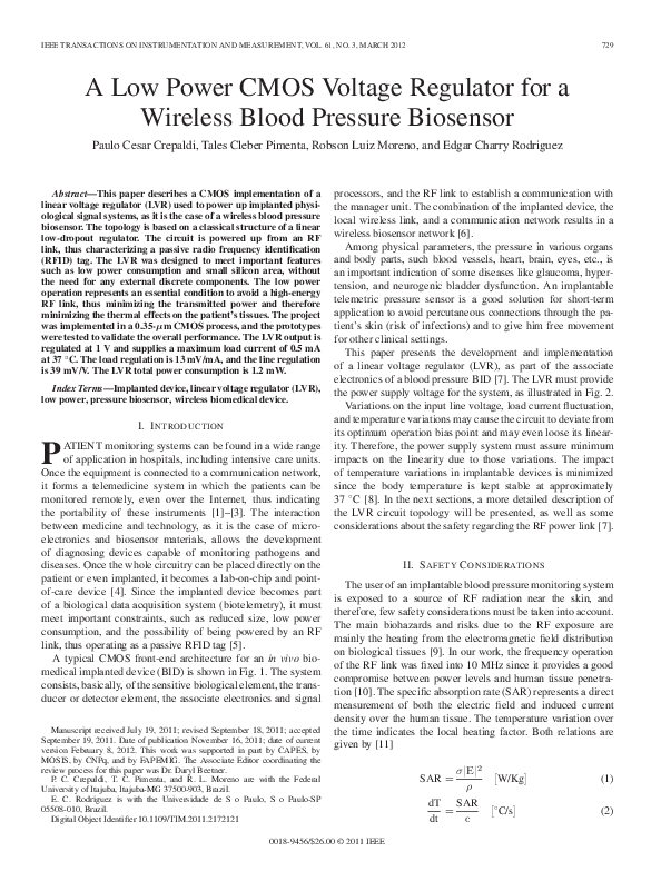
A typical CMOS front-end architecture for an in vivo biomedical implanted device (BID) is shown in Fig. 1. The system
consists, basically, of the sensitive biological element, the transducer or detector element, the associate electronics and signal
P
Manuscript received July 19, 2011; revised September 18, 2011; accepted
September 19, 2011. Date of publication November 16, 2011; date of current
version February 8, 2012. This work was supported in part by CAPES, by
MOSIS, by CNPq, and by FAPEMIG. The Associate Editor coordinating the
review process for this paper was Dr. Daryl Beetner.
P. C. Crepaldi, T. C. Pimenta, and R. L. Moreno are with the Federal
University of Itajuba, Itajuba-MG 37500-903, Brazil.
E. C. Rodriguez is with the Universidade de São Paulo, São Paulo-SP
05508-010, Brazil.
Digital Object Identifier 10.1109/TIM.2011.2172121
processors, and the RF link to establish a communication with
the manager unit. The combination of the implanted device, the
local wireless link, and a communication network results in a
wireless biosensor network [6].
Among physical parameters, the pressure in various organs
and body parts, such blood vessels, heart, brain, eyes, etc., is
an important indication of some diseases like glaucoma, hypertension, and neurogenic bladder dysfunction. An implantable
telemetric pressure sensor is a good solution for short-term
application to avoid percutaneous connections through the patient’s skin (risk of infections) and to give him free movement
for other clinical settings.
This paper presents the development and implementation
of a linear voltage regulator (LVR), as part of the associate
electronics of a blood pressure BID [7]. The LVR must provide
the power supply voltage for the system, as illustrated in Fig. 2.
Variations on the input line voltage, load current fluctuation,
and temperature variations may cause the circuit to deviate from
its optimum operation bias point and may even loose its linearity. Therefore, the power supply system must assure minimum
impacts on the linearity due to those variations. The impact
of temperature variations in implantable devices is minimized
since the body temperature is kept stable at approximately
37 ◦ C [8]. In the next sections, a more detailed description of
the LVR circuit topology will be presented, as well as some
considerations about the safety regarding the RF power link [7].
II. S AFETY C ONSIDERATIONS
The user of an implantable blood pressure monitoring system
is exposed to a source of RF radiation near the skin, and
therefore, few safety considerations must be taken into account.
The main biohazards and risks due to the RF exposure are
mainly the heating from the electromagnetic field distribution
on biological tissues [9]. In our work, the frequency operation
of the RF link was fixed into 10 MHz since it provides a good
compromise between power levels and human tissue penetration [10]. The specific absorption rate (SAR) represents a direct
measurement of both the electric field and induced current
density over the human tissue. The temperature variation over
the time indicates the local heating factor. Both relations are
given by [11]
0018-9456/$26.00 © 2011 IEEE
SAR =
σ|E|2
ρ
dT SAR
=
dt
c
[W/Kg]
[◦ C/s]
(1)
(2)
�730
IEEE TRANSACTIONS ON INSTRUMENTATION AND MEASUREMENT, VOL. 61, NO. 3, MARCH 2012
Fig. 1. Simplified diagram of an RFID BID.
Fig. 2. Block diagram of the blood pressure monitoring system.
where E is the incident electric field intensity (rms) and σ,
ρ, and c represent the conductivity, the human tissue mass
density, and the specific heat capacity, respectively, at the
implant location. Based on expressions (1) and (2), a safe value
for the power transferred by the RF link is 10 mW/cm2 [12].
The LVR power dissipation should be taken as just 10% of
it, corresponding to 1 mW, which represents twice as much
as required by the subsystems (0.5 mW). Reported voltage
regulators for implanted devices list a power dissipation range
that can be as high as tens of milliwatts [13].
The circuit topology and its components will be detailed
next, as well its frequency stability, which reveals an unconditional stable system.
III. LVR C IRCUIT T OPOLOGY
The classic topologies designed to provide stable power supply voltage are the linear and the switched regulators. Switched
regulators present a complex topology, mainly due to its control
systems, and generally require more power consumption and
larger silicon area. Additionally, it provides more noise at the
regulated output due to its switched operation [14].
The low-dropout (LDO) voltage regulator is one of the
most popular power converter used in power management
[15], [16] and is more suitable for implanted systems. In the
linear regulator, the output voltage is monitored and compared
to a voltage reference through an error amplifier [usually an
operational transconductance amplifier (OTA)]. The amplifier
output acts directly on the pass element in such a way that,
during its normal operation, there should be no fluctuations
on the output voltage. The pass element can be implemented
using bipolar or MOS transistors. Since a MOS transistor is
controlled by its gate voltage, it offers the advantage of smaller
power consumption and, consequently, higher efficiency for the
voltage regulator. The MOS transistor can be either N or P type.
The NMOS transistor requires a gate voltage higher than the
source voltage, and therefore, a charge pump may be necessary
to increase the voltage level. The proper choice for low-voltage
systems, such as implantable devices, is the use of a PMOS
LDO [17], [18] since its gate voltage is smaller than the source
voltage. An NMOS LDO without charge pump is reported in
[19] using native transistors (zero threshold) and an internal
capacitor to improve the stability, at the expense of two external
capacitors. Fig. 3 illustrates the contribution presented in this
work, by the introduction of a source follower stage (transistor
MNFOL ) and the alternative implementation of the resistive
sampler (R1 and R2 ). The resistive sampler was replaced by
a single MOS transistor along with a grounded MOS resistor
(biasing from transistor MNAUX ).
In the proposed circuit, the load capacitance (CL ) represents
the internal capacitance of the subsystems that are powered
up by the regulator (blood pressure microsensor, signal conditioner, processing unit, and transmitter). The input voltage
comes from the RF link after rectification and filtering. Finally,
the current source IL represents the overall current consumption
of the powered subsystems. The nominal values adopted for the
design are based on the actual subsystem (blood pressure microsensor, signal conditioner, processing unit, and transmitter)
requirements. The supply voltage goal is 1 V for a maximum
current load of 0.5 mA. Consequently, the total power required
�CREPALDI et al.: LOW POWER CMOS VOLTAGE REGULATOR FOR A WIRELESS BLOOD PRESSURE BIOSENSOR
Fig. 3.
Simplified diagram of the proposed LVR.
by the remaining subsystems is 0.5 mW. The source follower
stage (transistor MNFOL ) was added in order to provide stability to the LVR system. The rectifier, voltage references, OTA,
and the sampler will be discussed next.
IV. F RONT-E ND I NTERFACE
The front-end interface is presented is Fig. 4. The rectifier
was implemented in the chip. The use of regular diodes is
prohibitive due to the high frequency circuit operation. The
NMOS rectifier shows a good performance and has the advantage of being totally compatible with the CMOS digital
technology [20]. The cross gate rectifier structure suppresses
the threshold voltage drop of the switching transistors (MN1
and MN2 ). Additionally, the drain–source voltage VDS(ON) can
be minimized by proper W/L aspect ratio.
Transistors MN3 and MN4 cause the larger voltage drop
since they operate as diodes. Nevertheless, since they are
NMOS, their voltage drop is smaller than that of PMOS. In
the technology used in this project, the threshold voltage is
approximately 520 mV. This smaller voltage represents an
improvement on the rectifier efficiency [21].
The average voltage at the rectifier output (VRET ), which
is the LVR input voltage (VIN ), is fixed in 2.2 V in order
to operate the voltage references circuit, to be presented in
Section VI. The capacitive filter (CFILT ) was implemented
using a poly–insulator–poly capacitor and was designed to provide a ripple voltage of ≈ ±10% (2 V a 2.4 V) at a maximum
load current condition of 0.5 mA.
Fig. 5 shows the simulation results for the rectifier, and
Table I compares with measured values.
V. OTA
The OTA must present few optimized features to improve
the overall LVR performance. It must present a low offset
731
voltage (ViO ) since it affects directly the output voltage through
the control loop, as it can be modeled as a voltage source
in series with VREF . Additionally, ViO must present a low
thermal drift, even though it can be discarded in this project
due to the fairly stable human temperature. The power supply
rejection ratio (PSRR) must be maximized to avoid propagating
unregulated power supply ripple to the output. The open-loop
gain (AOL ) must be maximized to assure proper closed-loop
operation. In this design, the OTA load is purely capacitive,
represented by the input gate capacitance of the pass transistor
MPPASS . The OTA circuit is presented in Fig. 6, and it is
implemented as a self-biased folded cascode [22]–[25]. The
cascode topology has the advantages of improved PSRR and
presents a dominant pole that is determined only by the load
capacitance. The self-biased cascode also represents a good
solution to minimize silicon area since it does not need any
additional biasing circuitry. The power consumption of the OTA
is kept as low as possible to avoid degrading the efficiency
of the LVR. The OTA layout was carefully developed using a
centroid configuration to minimize any offset voltage. Table II
summarizes the main OTA-measured parameters. The load capacitance (CL ≈ 30 pF) represents the sum of all capacitances
at node OUT(OTA) .
The rail-to-rail topology needs an extra circuitry to compensate the gm variations due the PMOS and NMOS differential
input pairs. The frequency response of the OTA is directly
proportional to gm. However, as will be seen later on item 8,
evaluating the frequency response of the LVR, these variations
are not so significant provided that a pole splinting locates the
dominant pole and unit frequency gain at least three decades
before the other poles of the system. The advantage of the
absence of the gm compensation circuitry is less silicon area
and additional power dissipation.
VI. LVR VOLTAGE R EFERENCES
The LVR requires two voltages references, VG and VREF .
The VG reference is necessary to bias the source follower stages
represented by MNFOL and MNAUX . The VREF reference is
used, on the closed-loop system, to obtain the LVR output
�
�
R1
VOUT = 1 +
(3)
VREF .
R2
Bandgap references are generally used in voltage regulator
designs. There are alternative circuits capable of obtaining
low voltage and high accuracy; nevertheless, those approaches
may require components not readily available in CMOS technology (additional fabrications steps), or CMOS transistor on
subthreshold operation, or floating gate or even need of trimming [26]–[28]. Since the circuit is intended to be used in
an implanted device, the temperature range is very small, and
therefore, it is not taken into account. The reference voltage
sensitivity assumes the major factor quality. Fig. 7 presents the
proposed topology that is simple, requires small silicon area
(0.003 mm2 ), and requires just a few microwatts.
The core of this reference circuit is the self-biased current
mirror composed by MN1 , MP1 , MP2 , and Q1 . The use of
�732
IEEE TRANSACTIONS ON INSTRUMENTATION AND MEASUREMENT, VOL. 61, NO. 3, MARCH 2012
Fig. 4. LVR front-end interface.
TABLE II
OTA-MEASURED PARAMETERS
Fig. 5. Rectifier simulation results for average value and ripple.
TABLE I
RECTIFIER : S IMULATED AND M EASURED VALUES
Fig. 7.
Proposed voltage reference circuit.
the parasitic PNP bipolar transistor Q1 in a CMOS digital
technology is justified since it offers a well-known VBE voltage
(approximately 0.676 V for this circuit) and its corresponding
temperature behavior. To obtain higher voltage VG , other current mirrors and successive cascade of bipolar transistor are
used. A 2-V value is needed to bias the source follower stage
(MNFOL ) and the auxiliary voltage follower MNAUX . This
voltage reference is obtained by
VG = VEB (Q2 )+VEB (Q3 )+VEB (Q4 ) = 3VEB (Q1 ) ≈ 2[V].
(4)
Fig. 6. OTA circuit.
Voltage VREF is derived from VBE of transistor Q2 and
uses a composite structure of two MOS transistors, MN2 and
�CREPALDI et al.: LOW POWER CMOS VOLTAGE REGULATOR FOR A WIRELESS BLOOD PRESSURE BIOSENSOR
733
The self-biased current mirror was designed to operate with
a 4-µA base current, which is the MN1 transistor drain current.
Since the current mirrors are implemented by transistors MP3 ,
MP4 , MP5 , and MP6 (current gain of 1), the total current of
the reference generator circuit is 24 µA. Table III presents a
comparison of this work with others presented in the literature.
Since the circuit is intended to be used in an implanted
device, the temperature variation is negligible, and therefore,
it is not taken into account. The reference voltage sensitivity
assumes the major quality factor. The reference voltage sensitivities (considering the quiescent point Q) of VG and VREF
are given respectively by
REF
SV
VIN =
VIN
VREF
Q
∂VREF
∂VIN
Q
G
and SV
VIN =
VIN
VG
Q
∂VG
∂VIN
.
Q
(7)
The evaluated derivatives for VG and VREF are given as
Fig. 8.
UT λN
IDQ λN
∂VREF
G
=
and SV
VIN =3
2UT
2UT
∂VIN 1−
1−
VEB−VTHO(N)
(VEB−VTH0(N) )
Composite structure of two NMOS transistors to generate VREF .
(8)
Fig. 9.
Adjustment of the aspect ratio of MNREF1 by simulation.
MN3 . The composite MOS transistor improves the PSRR of
the voltage reference [29]. This topology is shown in Fig. 8.
Although the NMOS transistors, MNREF1 and MNREF2 ,
carry the same current ID , they are operated in weak inversion
and strong inversion, respectively. This condition leads to
ID (MNREF1 ) = ID (MNREF2 )
� �
�
�
VEB − VREF − VTH0(N)
W
IX
exp
L 1
nUT
�
�2
= βN VEB − VTH0(N) (1 + λN VREF ) .
where UT is the temperature equivalent voltage (kT/q), λN is
the channel modulation factor, and VTHO(N) is the threshold
voltage of the MOS transistor without the body effect factor.
It can be observed that VG voltage sensitivity is multiplied by
three due to the three voltages VBE added up along the way of
transistors Q2, Q3, and Q4.
Table IV provides a comparison of the sensitivity obtained
by using expressions (5) and (6), and the measured values.
The self-biased current mirror requires a start-up circuitry,
that it is implemented through capacitor CSTART and transistor
MSTART , as shown in Fig. 10. Simulation results (see Fig. 11)
show that the current ID (MSTART ) has a peak value of 160 µA
and vanishes to almost zero in less than 10 ns. Therefore, the
reference circuit is led to its operating point and avoids the
undesirable zero-state condition.
Figs. 12 and 13 show respectively the step response of the
two voltage references. As can be seen, their final values are
201.2 mV and 2.047 V that represent a small deviation from
the target values. VREF has an overshot with a duration of
approximately 1 µs, and VG takes 7 µs to reach its final value.
VII. S AMPLER C IRCUIT
(5)
By neglecting the term λN VREF , (5) can be rewritten as
� �
�2
βN VEB −VTH0(N)
� �
VREF = VEB −VTH0(N) −nUT ln
.
IX W
L 1
(6)
VREF is adopted as 200 mV. The aspect ratio of MNREF1
is adjusted by simulation to achieve that value, as illustrated in
Fig. 9.
Fig. 14 presents the sampler circuit. Since resistors are
avoided, mainly to save silicon area, R1 is implemented as
a MOS diode (transistor MN2 ), and R2 is implemented by
grounding a MOS resistor [33]. The use of the source follower transistor MNAUX guarantees that the MOS resistors
are isolated from VIN , thus avoiding a significant transference
of ripple voltage to the output line. MNAUX also imposes a
smaller effective voltage to the MOS resistor, thus reducing the
sampling current. The relationship R1 /R2 is optimized by the
adjustments of the aspect ratio of transistor MN2 .
The sampler circuit current IRES is designed to be ≈1% of
the maximum current load (≈5 µA).
�734
IEEE TRANSACTIONS ON INSTRUMENTATION AND MEASUREMENT, VOL. 61, NO. 3, MARCH 2012
TABLE III
COMPARISON W ITH OTHER R EFERENCES
TABLE IV
REFERENCE VOLTAGE S ENSITIVITY
Fig. 12.
Voltage reference VREF step response.
Fig. 13.
Voltage reference VG step response.
Fig. 14.
Sampler circuit.
Fig. 10. Inset of start-up circuit.
Fig. 11. Simulation of the start-up current.
By using the following relations, it is possible to determine
the values of R1 and R2 :
�
�
R1
R1
=4
(9)
1V = 1 +
0, 2V ⇒
R2
R2
1V = IRES (R1 + R2 ) ⇒ R1 + R2 = 200 KΩ.
(10)
The equation system composed of (9) and (10) is solved to
R1 = 160 KΩ and R2 = 40 KΩ.
�CREPALDI et al.: LOW POWER CMOS VOLTAGE REGULATOR FOR A WIRELESS BLOOD PRESSURE BIOSENSOR
735
Fig. 15. Classic PMOS LDO with discrete frequency compensation scheme.
The aspect ratio of MN1 was adjusted in order to set IRES
as close as to the target value of 5 µA. The PMOS array
and transistor MNAUX have also their aspect ratio adjusted
by simulation in order to minimize current consumption. The
measured current consumption of the PMOS transistor array is
2.94 µA, and the current IRES is 5.2 µA. Thus, the equivalent
resistor R2 is approximately 38.5 KΩ, and R1 is approximately
153.8 KΩ.
Fig. 16. Frequency response of a PMOS LDO regulator with external compensation capacitor.
VIII. S TABILITY A NALYSIS
The use of an LDO circuit requires a stability analysis
since it forms a closed-loop system. The frequency response
is degraded by the presence of two poles in addition to the
dominant pole that can lead an unstable system condition. It
is necessary to add a zero between these two poles to achieve
frequency compensation. The insertion of this zero is normally
done by adding a discrete electrolytic capacitor (CCOMP ) at the
output node that also contributes with an additional resistance
RESR (see Fig. 15). Also, ROTA is the output resistance of the
transconductance amplifier, CGPASS is the gate capacitance of
the PMOS pass transistor, and RDS is the channel resistance of
the PMOS pass transistor.
The frequencies of these poles and zero are given by [34]
fP0 =
−1
−1
≈
2π(RDS + RESR ).CCOMP
2πRDS CCOMP
(11)
fP1 =
−1
−1
≈
2π(RDS //RESR )CL
2πRESR CL
(12)
−1
2πRESR CCOMP
−1
.
=
2πROTA CGPASS
fZ0 =
(13)
fP2
(14)
Equation (11) shows that the frequency of the dominant pole
depends on the drain–source resistance, which in turn depends
on the drain current. As a consequence, the dominant pole
can change its position according to the load. To overcome
this situation, the zero must follow the pole. It is common to
establish not only a single value for RESR but a range of values
as a function of load current.
Fig. 16 presents the frequency response of a PMOS LDO.
The use of an external capacitor, such as an electrolytic capacitor, is prohibitive for an implantable device. The literature provides many contributions to solve the LDO stability
Fig. 17. Proposed topology to set a dominant pole in the LVR system.
problem. Few approaches maintain the external capacitor and
modify the internal feedback loop by using buffers [35] and
Miller compensation capacitor [36]. Other approaches insert an
internal zero, discarding the compensation capacitor, by using
controlled sources and even Miller compensation [37].
The solution proposed in this work is the introduction of a
source follower (MNFOL ) stage in between the input voltage
and the LDO block, and the removal of the compensation
capacitor CCOMP , as shown in Fig. 17. This stage maintains
the PMOS pass transistor in the triode region (small values
for VDS ).
To investigate the stability of the regulator, an open-loop
analysis is necessary to determine the loop gain Aβ. Fig. 18
shows the regulator with open feedback loop point, and in
Fig. 19, the OTA and the MPPASS are replaced by their smallsignal counterparts.
The loop gain can be stated by
Aβ = −
vr
.
vx
(15)
The total load resistance is minimized by the low value of
rds , so the drain–gate voltage gain of MPPASS is
K=−
vout
= −gmPASS rDS .
vgs
(16)
�736
IEEE TRANSACTIONS ON INSTRUMENTATION AND MEASUREMENT, VOL. 61, NO. 3, MARCH 2012
Fig. 20.
Frequency response of the proposed LVR.
Fig. 21.
Microphotography of the chip.
Fig. 18. Proposed voltage regulator highlighting the open-loop point.
Fig. 19. Small signal circuit to determine the loop gain.
The output voltage is
vout = −
gmPASS .rds gmOTA ro
1+
S
p1
S
p2
1+
vx .
(17)
Moreover, vr , considering that rid is much larger than R2 , is
vr = vout
R2
.
R1 + R2
(18)
Combining (17) and (18), the loop gain is
Aβ =
gmPASS .rds gmOTA ro
1+
S
p1
1+
S
p2
R2
.
R1 + R2
(19)
IX. LVR M EASUREMENTS
By properly adjusting the transistor aspect ratio, rds can be
designed to be smaller than resistors R1 and R2 of the sampling
circuit. rds was chosen to be less than 100 Ω for our LVR. The
system poles, under the new approach, are
p1 =
1
and
(Cgd + CL )rds
p2 =
1
.
[Co + Cgs + Cgd (1 + gmPASS rds )] ro
The derived values for fP0 and fP2 are 318 MHZ and 133 HZ ,
respectively, resulting in a unit frequency gain fUG of 620 KHZ .
Fig. 20 presents the frequency response of the proposed LVR.
The source follower stage is disadvantageous for the system
since it represents additional power consumption. Nevertheless,
the system does not require the external components to become stable, thus representing an important advantage for an
implantable system.
(20)
The pole p2 is the dominant one since ro , in the range of
megohms, can be at least 104 times greater than rds that is in the
range of a tenth of an ohm. Therefore, the frequency stability
of the regulator is a function of the OTA design, the geometric
aspect ratio of MPPASS , and the load. As an application specific
integrated circuit (ASIC) application, the load current (IL ), resistance (RL ), and capacitance (CL ) can be stated as constants.
The LVR was implemented in a Taiwan Semiconductor Manufacturing Company 0.35-µm CMOS technology through MOSIS. Fig. 21 shows the microphotography
of the prototype, and Fig. 22 shows the basic circuit used
to characterize the most important features. The antennas are
artisanal and are kept 5 cm away from each other. The transmitter is implemented by an RF generator, and the chip input
voltage is monitored to avoid exceeding 3.6 V (maximum value
allowed by the technology). Table V summarizes the main
parameter measurements on the LVR. The dynamic behavior
of the LVR is depicted in Fig. 23 where an input step signal
is applied at a load current of 0.5 mA and a capacitive load
of 30 pF. It can be seen that the LVR output voltage is stable,
without any overshoot, with a setup time of just 16 µs. The
transient response of the LVR circuit indicates a bounded-inputbounded-output system. Table VI shows a comparison of our
work with previous reported regulators.
�CREPALDI et al.: LOW POWER CMOS VOLTAGE REGULATOR FOR A WIRELESS BLOOD PRESSURE BIOSENSOR
737
Fig. 22. Basic circuit for the LVR measurements.
TABLE V
LVR-MEASURED PARAMETERS
TABLE VI
COMPARISON W ITH P REVIOUS R EPORTED R EGULATORS
Fig. 23. Step function response at IL = 0,5 mA and T = 37 ◦ C.
A set of 5000 runs of Monte Carlo simulation was conducted
to evaluate the impact of process variation on the LVR output
voltage, and the result is presented in Fig. 24. The VOUT mean
value is 0.992 V, and the standard deviation is 80.6 mV.
X. C ONCLUSION
This paper has presented an LVR for physiological monitoring systems that is powered by an RF link. The regulator was
Fig. 24. Monte Carlo analysis of the LVR output voltage.
designed specifically to meet important requirement conditions,
such as low power consumption, low silicon area, and the
absence of external discrete components. The output voltage
is regulated to 1 V at a maximum load current of 0.5 mA,
and the dissipated power is 1.2 mW. The load regulation is
13 mV/mA, and the line regulation is 39 mV/V. The dynamic
behavior shows an unconditionally stable response.
�738
IEEE TRANSACTIONS ON INSTRUMENTATION AND MEASUREMENT, VOL. 61, NO. 3, MARCH 2012
R EFERENCES
[1] W. G. Scanlon, N. E. Evans, G. C. Crumley, and Z. M. McCreesh, “Low
power radio telemetry: The potential for remote patient monitoring,”
J. Telemed. Telecare, vol. 2, no. 4, pp. 185–191, 1996.
[2] R. Puers, in Proc. Implantable Sens. Syst., DISens Symp. Book, 2005,
vol. 2.6, pp. 1–14.
[3] M. Miyazaki, “The future of e-Health—Wired or not wired,” in Proc.
Business Briefing—Hospital Engineering & Facilities Management,
2005, pp. 1–5.
[4] J. Colomer-Farrarons, P. Miribel-Catala, I. Rodriguez, and J. Samitier,
“CMOS front-end architecture for in-vivo biomedical implantable devices,” in Proc. 35th Annu. Conf. IECON, pp. 4401–4408.
[5] J. Landt, “The history of RFID,” IEEE Potentials, vol. 24, no. 4, pp. 8–11,
Oct./Nov. 2005.
[6] M. Guennoun, M. Zandi, and K. El-Khatib, “On the use of biometrics to
secure wireless biosensor networks,” in Proc. 3rd Int. Conf. Digit. Idenfier
ICTTA, pp. 1–5.
[7] P. C. Crepaldi, T. Pimenta, R. Moreno, and E. Rodriguez, “A CMOS
linear power supply for a wireless biomedical sensor,” in Proc. IEEE Int.
Workshop MeMeA, 2010, pp. 97–101.
[8] P. A. Mackowiak, S. S. Wasserman, and M. M. Levine, “A critical appraisal of 98.6 ◦ F, the upper limit of the normal body temperature, and
other legacies of Carl Reinhold,” August Wunderlich. JAMA, vol. 268,
no. 12, pp. 1578–1580, Sep. 23–30, 1992.
[9] J. M. Osepchuk and R. C. Petersen, “Safety standards for exposure to
RF electromagnetic fields,” IEEE Microw. Mag., vol. 2, no. 2, pp. 57–69,
Jun. 2001.
[10] C. Sauer, M. Stanacevic, G. Cauwenberghs, and N. Thakor, “Power
harvesting and telemetry in CMOS for implanted devices,” IEEE
Trans. Circuits Syst. I, Reg. Papers, vol. 52, no. 12, pp. 2605–2613,
Dec. 2005.
[11] A. Pradier, D. Lautru, M. F. Wong, H. V. Fouad, and J. Wiart, “Rigorous
evaluation of Specific Absorption Rate (SAR) induced in a multilayer
biological structure,” in Proc. Eur. Conf. Wireless Technol., Oct. 3/4, 2005,
pp. 197–200.
[12] G. Lazzi, “Thermal effects of bioimplants,” IEEE Eng. Med. Biol. Mag.,
vol. 24, no. 5, pp. 75–81, Sep./Oct. 2005.
[13] C. Zheng and D. Ma, “Design of monolithic low dropout regulator for
wireless powered brain cortical implants using a line ripple rejection
technique,” IEEE Trans. Circuits Syst. II, Exp. Briefs, vol. 57, no. 9,
pp. 686–690, Sep. 2010.
[14] G. A. Rincon-Mora and P. E. Allen, “Study and design of low dropout regulators,” Sch. Elect. Comput. Eng., Georgia Inst. Technol.,
Atlanta, GA.
[15] G. A. Rincon-Mora, “Active multiplier in Miller-compensated circuits,” IEEE J. Solid-State Circuits, vol. 35, no. 1, pp. 26–32,
Jan. 2000.
[16] G. A. Rincon-Mora and P. Allen, “A low-voltage, low quiescent current,
low drop-out regulator,” IEEE J. Solid-State Circuits, vol. 33, no. 1,
pp. 36–44, Jan. 1998.
[17] T. Kugelstadt, “Fundamental theory of PMOS low-dropout voltage regulators,” Texas Instrum. Inc., Dallas, TX, Application Note SLVA068,
Apr. 1999.
[18] C. Simpson, “A user’s guide to compensating low-dropout regulators,” in
Proc. Wescon, Nov. 4–6, 1997, pp. 270–275.
[19] M. M. Ahmadi and G. A. Jullien, “A wireless implantable microsystem
for continuous blood glucose monitoring,” IEEE Trans. Biomed. Circuits
Syst., vol. 3, no. 3, pp. 169–180, Jun. 2009.
[20] M. Ghovanloo and K. Najafi, “Fully integrated wideband high-current
rectifiers for inductively powered devices,” IEEE J. Solid-State Circuits,
vol. 39, no. 11, pp. 1976–1984, Nov. 2004.
[21] J. Hu and H. Min, “A low power and high performance analog front
end for passive RFID transponder,” in Proc. 4th IEEE Workshop Autom.
Identification Adv. Technol., Oct. 17/18, 2005, pp. 199–204.
[22] B. G. Song, O. J. Kwon, I. K. Chang, H. J. Song, and K. D. Kwack, “A
1.8 V self-biased complementary folded cascode amplifier,” in Proc. 1st
IEEE ASICs, AP-ASIC , Aug. 23-25, 1999, pp. 63–65.
[23] P. Mandal and V. Visvanathan, “Design of high performance two stage
CMOS cascode op-amps with stable biasing,” in Proc. 9th Int. Conf. VLSI
Design, Jan. 3–6, 1996, pp. 234–237.
[24] P. Mandal and V. Visvanathan, “A self biased high performance folded
cascode CMOS op-amp,” in Proc. 10th Int. Conf. VLSI Design, Jan. 4–7,
1997, pp. 429–434.
[25] V. Ceperic, Z. Butkovic, and A. Baric, “Design and optimization of
self-biased complementary folded cascode,” in Proc. IEEE MELECON,
May 16–19, 2006, pp. 145–148.
[26] W. Jianping, L. Xinquan, L. Yushan, Z. Jie, and G. Xiaofeng, “A novel
low-voltage low-power CMOS voltage reference based on subthreshold
MOSFETs,” in Proc. 6th Int. Conf. ASIC, ASICON, Oct. 24–27, 2005,
vol. 1, pp. 369–373.
[27] B. K. Ahuja, H. Vu, C. A. Laber, and W. H. Owen, “A very high precision
500 nA CMOS floating-gate analog voltage reference,” IEEE J. SolidState Circuit, vol. 41, no. 10, pp. 572–573, May 12, 2005.
[28] C. W. Chang, T.-Y. Lo, C.-M. Chen, K.-H. Wu, and C.-C. Hung, “A low
power CMOS voltage reference circuit based on subthreshold operation,”
in Proc. IEEE ISCAS, May 27–30, 2007, pp. 3844–3847.
[29] L. H. C. Ferreira and T. C. Pimenta, “A week inversion composite
MOS transistor for ultra-low-voltage and ultra-low-power applications,”
in Proc. 13th Int. Conf. Mixed Design Integr. Circuits Syst. Gdynia,
Jun. 2006, pp. 1–4.
[30] A. Becker-Gomez, T. Lakshmi Viswanathan, and T. R. Viswanathan, “A
low-supply-voltage CMOS sub-bandgap reference,” IEEE Trans. Circuits
Syst. II, Exp. Briefs, vol. 55, no. 7, pp. 609–613, Jul. 2008.
[31] K. N. Leung and P. K. T. Mok, “A sub-1-V 15- ppm/◦ C CMOS bandgap
voltage reference without requiring low threshold voltage device,” IEEE
J. Solid-State Circuits, vol. 37, no. 4, pp. 526–530, Apr. 2002.
[32] G. De Vita and G. Ianaccone, “A sub-1-V 10- ppm/◦ C nanopower voltage reference generator,” IEEE J. Solid-State Circuits, vol. 42, no. 7,
pp. 1536–1542, Jul. 2007.
[33] K. Dejhan, N. Suwanchatree, P. Prommee, S. Piangprantong, and
I. Chaisayun, “A CMOS voltage-controlled grounded resistor using a
single power supply,” in Proc. IEEE ISCIT, Oct. 26–29, 2004, vol. 1,
pp. 124–127.
[34] A. Rogers, “Stability analysis of low-dropout linear regulators with a
PMOS pass element,” Analog Applications Journal, pp. 10–12, Dallas,
TX, Aug. 1999.
[35] C. Stanescu, “Buffer stage for fast response LDO,” in Proc. 8th ICSICT,
Sep. 28/Oct. 2, 2003, vol. 2, pp. 357–360.
[36] W. Huang, S.-H. Lu, and S.-I. Liu, “CMOS low dropout regulator with
single Miller capacitor,” Electron. Lett., vol. 42, no. 4, pp. 216–217,
Feb. 2006.
[37] W. Huang, S.-H. Lu, and S.-I. Liu, “A capacitor-free CMOS low dropout
regulator with slew rate enhancement,” in Proc. Int. Symp. VLSI Design,
Autom. Test, Apr. 2006, pp. 1–4.
[38] Y. P. Tsividis, Operation and Modeling of the MOS Transistor. New
York: McGraw-Hill, 1999.
[39] T. Y. Man, P. K. T. Mok, and M. Chan, “A high slew-rate push–pull output
amplifier for low-quiescent current low-dropout regulators with transientresponse improvement,” IEEE Trans. Circuits Syst. II, Exp. Briefs, vol. 54,
no. 9, pp. 755–759, Sep. 2007.
[40] S. Lau, P. K. T. Mok, and K. N. Leung, “A low-dropout regulator for SoC
with Q-reduction,” IEEE J. Solid-State Circuits, vol. 42, no. 3, pp. 658–
664, Mar. 2007.
[41] R. J. Milliken, J. Silva-Martıacute;nez, and E. Sánchez-Sinencio, “Full onchip CMOS low-dropout voltage regulator,” IEEE Trans. Circuits Syst. I,
Reg. Papers, vol. 54, no. 9, pp. 1879–1890, Sep. 2007.
Paulo Cesar Crepaldi received the B.Sc., M.Sc.,
and Ph.D. degrees in electrical engineering from the
Universidade Federal de Itajuba, Itajuba, Brazil, in
1984, 1992, and 2009, respectively.
Since 1985, he has been a Professor with Universidade Federal de Itajuba.
Tales Cleber Pimenta received the B.S. and M.S.
degrees in electrical engineering from the Universidade Federal de Itajuba, Itajuba, Brazil, in 1985 and
1988, respectively, and the Ph.D. degree from the
Ohio University, Athens, in 1992.
Since 1985, he has been a Professor with the
Universidade Federal de Itajuba. He was a Visiting
Scholar at The Ohio State University, Columbus,
and Virginia Polytechnic and State University,
Blacksburg, in 1997 and 2005, respectively.
�CREPALDI et al.: LOW POWER CMOS VOLTAGE REGULATOR FOR A WIRELESS BLOOD PRESSURE BIOSENSOR
Robson Luiz Moreno received the B.S. degree in
electrical engineering from the Universidade Federal
de Itajuba, Itajuba, Brazil, in 1988, the M.Sc. degree from the Universidade de Campinas, Campinas,
Brazil, in 1996, and the Ph.D. degree from the Universidade de São Paulo, São Paulo, Brazil, in 2002.
Since 2002, he has been a Professor with the
Universidade Federal de Itajuba.
739
Edgar Charry Rodriguez received the B.S. degree
in electrical engineering from the Universidad Del
Valle, Cali, Colombia, in 1962, the M.Sc. degree
from Instituto Politécnico Nacional de México,
México City, México, in 1970, and the Ph.D. degree
from the Universidade de São Paulo (USP), São
Paulo, Mexico, in 1974.
He is currently a Researcher with USP. He has
experience in the area of integrated circuits, mainly
in CMOS, and pressure sensors.
�
 Tales Pimenta