The Optical Sensor Mote: A novel device
for enabling next generation Wireless
Sensor Networks.
by
Hazem Abdul’Aal A. M. Awad
A Thesis
presented to the University of Strathclyde in fulfilment
of the requirements for the degree of Doctor of
Philosophy
in
Department of Electronic and Electrical Engineering
Centre for Intelligent Dynamic Communications
July 2013
1
�Declaration
This thesis is the result of the author’s original research. It has
been composed by the author and has not been previously
submitted for examination which has led to the award of a
degree.
The copyright of this thesis belongs to the author under the
terms of the United Kingdom Copyright Acts as qualified by
University
of
Strathclyde
Regulation
3.50.
Due
acknowledgement must always be made of the use of any
material contained in, or derived from, this thesis.
Hazem Abdul’Aal A. M. Awad
July 2013
2
�Dedication
To my dad and all my family
3
�Acknowledgments
First, I would like to acknowledge and sincerely thank my two supervisors; Dr. Ivan
Andonovoic and Dr. Trevor J. Hall, as well as Dr. Imad Hasan, Dr. Khaled Mnaymne,
and Dr. Sawsan Majid who have helped, guided and inspired me throughout my
doctoral studies. Their support, encouragement, and kindness have been instrumental
in helping me to bring this work to life.
I would like to express my sincere thanks to the following people: Dr. Sofia Paredes
for her guidance and with the WSN prototype, Tom Davies (Technix by CBS) for his
outstanding help and support with CrystalWave (the primary photonic crystal
modelling tool), Nic Oliveri (lab manager) for his great help in and out of the lab,
Dan Deptuck and Patricia Greig (CMC), and my colleagues and friends: Dr. Robert
Radziwilowicz, Erin Knight and others. I would also like to thank my former
colleagues Hassan and Atousa Teimori and Dr. Degui Sun, Dr Mohamed Abdelalim,
Dr Jeremy Upham, Huesein Kotob, and Zahirul Alam.
I would also like to express my sincere thanks to all my great friends and colleagues,
in particular Ahmad Gharba, Ramy Waleed, Maysra Shams, Mohamed Syed, and
many others for all the help, laughter, shared memories, support and encouragement.
Finally and most importantly, I wish to offer my most sincere and heartfelt thanks
and gratitude to my amazing family: my father Abdul’Aal, my amazing siblings:
Magid, Heba, and Marwa Awad, and my extended family for all their tremendous
help, love, and encouragement thought my entire life.
4
�Abstract
Recent advances in micro-electronics and communications have fuelled research in
Wireless Sensor Networks (WSNs). WSNs are a collection of low power, low cost,
small form factor devices referred to as sensor motes interconnected in a random
manner to establish a network. Despite wide ranging research into a range of
applications, significant limitations stand in the way of utilizing WSNs to monitor
large scale/area environments.
Optical sensing techniques are well suited for monitoring a large variety of
environmental variables such as temperature, pressure, humidity, and gas
concentrations. However, traditional optical sensing techniques rely on bulky
solutions including spectroscopic equipment and fibre based approaches. On the
other hand, photonic crystals have caused a revolution in integrated optics as they
allow functionalities not possible before; however little has been reported on their
use as integrated optical sensors.
The research work combines the diverse but related fields of WSNs, integrated optics,
and Photonic Crystals. A novel platform, the optical sensor mote, is proposed and its
key building blocks are experimentally demonstrated as a feasibility study.
Specifically, multi-gas sensors based on the slow light phenomenon in photonic
crystal waveguides are theoretically and experimentally demonstrated. These sensors
can sense multiple gases without the need of any physical changes. They can also be
integrated with electronics to yield an optical sensor mote of small form factor which
is stable, multi-functional, and cost effective.
The optical sensor mote represents a significant step towards enabling the wide
spread use of WSNs to monitor large scale/area environments and providing a highly
integrated mote platform amenable to mass production and providing multi-functions.
5
�Table of Contents
Chapter 1 Introduction .............................................................................................. 8
1.1
Background .................................................................................................. 8
1.2
Motivation .................................................................................................. 14
1.2.1
The Optical Sensor Mote ................................................................... 16
1.3
Objectives .................................................................................................. 17
1.4
Summary of Contributions ......................................................................... 18
1.4.1
Publications ........................................................................................ 20
1.5
Structure of the Thesis ............................................................................... 20
Chapter 2 Optical Sensor Mote: Wireless Sensor Networks for environmental
monitoring 22
2.1
Background ................................................................................................ 22
2.2
ZigBee Standard......................................................................................... 24
2.3
WSN Application: Gas monitoring in mines ............................................. 26
2.4
A basic WSN for environmental monitoring ............................................. 28
2.4.1
Background and objective .................................................................. 28
2.4.2
Introduction to WSN .......................................................................... 29
2.4.3
WSN implementation......................................................................... 32
2.4.4
WSN Software: SimpleApp ............................................................... 34
2.4.5
WSN Software: Finite State Machine (FSM) .................................... 38
2.4.6
WSN: Typical Results........................................................................ 45
2.5
Conclusion ................................................................................................. 53
Chapter 3 Optical Sensor Mote: Photonic Crystal structures for Multi-Gas sensing
54
3.1
Background ................................................................................................ 54
3.2
Introduction to Photonic Crystal Theory ................................................... 54
3.2.1
Photonic Crystal Slabs ....................................................................... 62
3.3
Photonic Crystals and Gas Sensing ............................................................ 64
3.3.1
Photonic crystals as a versatile sensing platform ............................... 64
3.4
SOI Multi-Gas Photonic Crystal Sensor (MG-PhC) .................................. 80
3.4.1
Background ........................................................................................ 80
3.4.2
Material consideration ....................................................................... 80
3.4.3
Sensor Structure ................................................................................. 82
3.4.4
Theory of Operation ........................................................................... 83
3.4.5
Initial Design ...................................................................................... 88
3.4.6
FDTD Simulations ........................................................................... 103
3.4.7
Mask Design .................................................................................... 117
3.4.8
Experimental Results ....................................................................... 125
3.5
InP Multi-Gas Photonic Crystal Sensor (MG-PhC)................................. 143
3.5.1
Background ...................................................................................... 143
3.5.2
Initial Design .................................................................................... 143
3.6
Slow light InP Multi-gas Photonic Crystal Sensor .................................. 154
3.6.1
Background ...................................................................................... 154
3.6.2
Introduction to Slow Light in Photonic Crystals ............................. 156
3.6.3
Sensor Structure and Theory of Operation ...................................... 162
6
�3.6.4
FDTD Simulations ........................................................................... 164
3.6.5
MIT MPB Simulations: Frequency based approach. ....................... 169
3.6.6
Fabrication and Experimental Results ............................................. 179
3.7
Conclusions .............................................................................................. 194
Chapter 4 Conclusion and outlook: the Optical Sensor Mote .............................. 199
4.1
Summary and concluding remarks ........................................................... 199
4.2
Outlook and Future work ......................................................................... 203
References ................................................................................................................ 205
Buswell et al. 2008 S. C. Buswell et al., "Specific detection of proteins using
photonic crystal waveguides", Optics Express, Vol. 16, Issue 20, 2008, pp.
15949-15957. ....................................................................................................... 206
7
�Chapter 1
Introduction
1.1 Background
Sensors are everywhere and are a fundamental part of life. Sensors play a critical role
in all aspects of living organisms. The five senses that most humans enjoy are
enabled by extremely sophisticated biological sensors. A sensor can be defined as a
device that responds to a physical stimulus (as heat, light, sound, pressure,
magnetism, or a particular motion) and transmits a resulting impulse (as for
measurement or operating a control). Sensors are often closely associated with
actuators. An actuator can be defined as a device for moving or controlling
something.
Humans have created a variety of sensors to aid them in their life. Indeed, the topic
of Sensors is very vast and a large variety of sensors have been developed over time.
Often, sensors are classified according to their sensing mechanism, e.g.: mechanical,
biological, chemical, electrical, electronic, and optical to name a few. Within these
general classifications, many sub classifications exist as well.
In the sensor field, optical sensing techniques (and optical sensors) are ubiquitous.
They are used in a very wide variety of sensing applications including automotive,
military, avionics, environmental and biomedical applications to name a few
[Giancarlo et al. 2009]. Optical sensors can be generally classified into two
categories: 1. Free space sensors (which find wide applications in the areas of
spectroscopy and interferometry), and 2. Guided wave based sensors. Guided wave
8
�sensors can further be sub divided into: 2.1) Fibre based optic sensors and 2.2)
Integrated optic sensors.
While free space optical sensors were among the first optical sensors to be developed
and utilized effectively, they suffer from critical issues that limit their sensing
applications, particularly the limitations of line of sight and stringent alignment
requirements. These issues make them particularly susceptible to external
environmental perturbations which often affect the sensing operation.
Guided wave sensors do not suffer from the limitations of their free space counter
parts and have a number of inherent advantages including: immunity to electrical and
electromagnetic interference, flexibility in deployment (due to their small size and
guided nature), ruggedness (e.g. in resisting ionizing damage), and ease of interface
with optical communication systems [Giancarlo et al. 2009] .
The basic principle behind optical sensing with guided wave sensors is as follows:
light radiation that is trapped within the dielectric medium of an optical waveguide
responds to/is modulated by perturbation in the external environment (e.g.
temperature changes, gases, mechanical stresses and strains…etc). The resulting
effects of such external perturbation on the guided light radiation can often be used
to draw meaningful information about the perturbations themselves, in essence,
leading to the sensing of these external perturbations. The external perturbations
modulate the guided light in different ways, the most common being: amplitude
9
�(intensity) modulation, phase modulation, wavelength modulation, and polarization
modulation.
Fibre optic sensors are currently the most dominant and well developed form of
guided wave sensors. This is mainly attributed to the significant research and
development that fibre technology underwent (particularly to achieve very low
attenuation characteristics) for use in telecommunication applications and the
uniqueness of the development platform (fibres for telecommunication and sensing
applications are often made mainly from pure silica cores). This uniqueness (which
can also be viewed as lack of options from a material perspective) actually helped
focus the majority of the research efforts on producing very high quality and pure
silica which in turn accelerated the development of fibre technology for
telecommunication, and later, sensing applications. Furthermore, speciality fibre and
fibre structures for sensing has been developed such as Photonic Crystal Fibres
(PCF) and Long Period Optical Fibre Grating sensors (LPFG). Fibre optic sensors
have been developed to sense a variety of parameters: temperature, stress and
mechanical strains (e.g. for bridges and other infrastructure), biochemical detection
of gases and containments (e.g. in drinking water) to name a few.
The biggest draw back of fibre optic sensors is their size or more appropriately, their
bulky nature. This makes them difficult and costly to install and deploy as they have
to laid-out over the area to monitored (e.g. bridge) and limits their ability to be
networked (to form a network of sensors). Furthermore, fibre optic sensors do not
lend themselves well to integration with other electronic systems (which may be
10
�used for information processing) and only discrete integration is possible which leads
to bulky sensor solutions.
The aforementioned issues severely limit the application of fibre sensors in sensing
applications that require the monitoring of large scale areas. Examples include farm
monitoring (of both crops and cattle), mine monitoring (for dangerous build-up of
gases), forest monitoring (e.g. for fires) and so on. Integrated optical sensors provide
an alternative to fibre sensors in these types of applications (and potentially other
applications). There exists however, commercial fibre optics products based on
spectroscopic gas sensing technologies that have been successfully applied to
distributed sensing [OptoSniff]. These approaches utilize fibre cables to transmit data
from a large number of sensing points and provide real time and highly accurate
sensing capabilities of hazardous gases (methane and natural gas).
Integrated optic sensors operate using the same principle as their fibre sensors
cousins. They have, however, developed at a slower pace and for (initially) a
different set of applications. In particular, one of the main motivations for the
development of integrated optics was for use in multi functional circuits (which may
contain electronic components or be all-optical circuits). These circuits will be chip
size (i.e. a few cm or mm in dimension) and hold great promise for a wide array of
applications such as lab-on-chip and large scale (optical) sensor networks.
Integrated optics however, suffer from an interesting dilemma. Unlike fibre optics
which really has only one main material fabrication platform (i.e. high purity silica),
11
�there are many material options for integrated optics (and integrated optic sensors).
Some of these material fabrication platforms include: Silicon over Silica (Si over
SiO2), Indium Phosphide (InP), Gallium Arsenide (GaAs), polymers, and even liquid
crystals. Furthermore, currently, none of the available material fabrication platforms
have achieved dominance yet as the most favourable platform. Such a wide array of
material choices led to a slower progress in the field of integrated optics compared to
fibre optics while simultaneously offering a great deal of flexibility and a much
wider range of applications (including sensing).
Integrated optical sensors have a number of inherent advantages over their fibre optic
cousins including: much greater flexibility (thanks to greater material choices), very
small size (which makes them ideal for monitoring of large scale areas), and very
importantly, the potential for integration with other electronic (or even optical)
processing elements. That last point is of great importance because it opens the door
for the formation of a wireless network of (optical) sensors nodes/motes more
commonly called wireless sensor networks (WSN).
The research is a study into the viability of a specific family of integrated optic
sensors -photonic crystal refractive index (RI) sensors – and a characterisation of a
new subclass referred to as ‘slow light RI’ based sensors. The sensors offer the
potential for new performance advantages and may complement the currently
dominant form of optical sensors for chemical and biological detection based on
spectroscopy [Pergande et al. 2011; Passaro 2013].
12
�There are several slightly different definitions of a sensor mote [Sensor Mote a],
[Sensor Mote b], [Sensor Mote c]. The following general definition is adapted: “A
sensor mote/node is a node in a wireless sensor network that is capable of
performing some processing, gathering sensory information and communicating with
other connected nodes in the network.” [Sensor Mote d]. The sensor mote forms the
building block of WSN which are of increasing importance in the area of sensing.
WSN find many current applications in sensing. In particular, WSN are well suited
for environmental monitoring of large scale areas including: forest fires, landfills,
farms and cattle, structural monitoring (e.g. bridges, ships, and Aircraft), Air
pollution (including monitoring of build up of dangerous gases in areas such as
mines), military and civilian security, and so on [Hall 2009a; Hall 2009b; WSN
Applications a; WSN Applications b]. Furthermore, WSN can include actuators as
well as sensors and so have the ability to monitor and manipulate the environment
(e.g. in industrial quality and control applications).
It can be argued that the big push in research and development of WSN is actually
one of the manifestations of humans to understand and manipulate their environment
to be more suitable for them or to achieve a certain set of outcomes. WSN are
enabled by many factors including: great advances in miniaturization of electronic
components, advances in miniaturized sensors (including integrated optic sensors),
and the rise of various communication protocols for the monitoring, analyzing and
processing of the sensor data (e.g. ZigBee).
13
�Despite the advances in WSN, several important issues remain which limit their
viability [Benini et al. 2006]. Some of these issues include: communication protocols
shortcomings, hardware issues, and safety issues. The issue that concerns us the most
in this research work however is the sensor mote itself. Specifically, the lack of an
appropriate sensing mechanism that is suitable for efficient and accurate monitoring
of a large class of important environmental phenomena (with the often additional
requirement of large scale / wide area monitoring). In fact, the primary motivation of
WSN is the monitoring of large scale / wide areas.
As stated earlier, optical sensing mechanisms are often among the most suitable for
the monitoring of various environmental conditions (e.g. temperature, pollution,
biological and chemical pollution). It therefore makes a great deal of sense for the
sensor mote (which forms the building block of the WSN) to utilize optical sensing
as its primary sensing mechanism. Currently however, this is not the case.
Therefore, it is proposed that the missing piece to overcoming some of the most
critical shortcomings of WSNs is the optical sensor mote: a sensor mote that uses
optical sensing as its primary sensing mechanism. Such an optical sensor mote is
what this research work discusses.
1.2 Motivation
The preceding section makes it clear that improving the sensor mote itself (primarily,
by using optical sensing mechanisms) is a potentially powerful approach to
overcoming some of the main challenges that WSNs currently face and significantly
14
�improving their capabilities and adoption. Ideally however, any improvements to the
sensor mote itself would NOT take away from its current advantages which include:
small size (or foot print), low cost of manufacturing, ease of mass production, ability
to communicate with other motes using wireless RF technology (which is critical for
cost effective deployment over a wide area), and signal processing capabilities. The
biggest drawback of current sensor motes is their sensing mechanisms which are
primarily not based on optics.
Purely optical approaches were initially investigated for the sensor mote. That is, the
sensing, transmission, and even signal processing will take place in the optical
domain. In essence, it was wished to extend the concept of optical wireless [Heatley
et al. 1998] to the WSN domain. In essence, the purely optical approach to the sensor
mote would be similar to the concept of optical wireless networks but specifically
tailored to environmental sensing as opposed to some of the more common
applications of current optical wireless research such as cellular over optical wireless
networks [Katz et al. 2006].
It was quickly discovered however, that there are many challenges currently facing
optical wireless systems in general. Furthermore, these issues increase when
applying and extending optical wireless concepts to the WSN domain. This is mainly
due to greater and more stringent requirements for the optical sensor mote, especially
the signal processing which will have to take place in the optical domain and such
technology, while currently existing in various forms [Awad 2006], is still in its
infancy and not practical for real world applications.
15
�Furthermore, current optical wireless networks are plagued with issues related to
path loss and alignment (to ensure line of sight operation). Additionally, the
workarounds to the line of sight challenges are challenging in of themselves,
particularly, when it is desirable to allow the sensor motes to communicate with each
other while monitoring, say livestock, forest fires, or even mine conditions (all of
which happen to be attractive WSNs applications). It quickly became clear that
alternative approaches are required to actually create an optical sensor mote that
solves the basic needs.
1.2.1 The Optical Sensor Mote
Based on the previous sections, the concept of the optical sensor mote is proposed.
This is a sensor mote that is similar to currently available sensor motes but makes
use of integrated optic sensors as its primary sensing mechanism while keeping all
other features the same as current sensor motes (including, using RF for
communication and electronics for signal processing).
In essence, the proposed optical sensor mote is based on the (hybrid) integration of
integrated optics and electronics technologies on the same chip/wafer [Rubenstein et
al. 2011; Wada 2008]. Each technology shall be utilized where it is best suited: RF
for wireless transmission (between the sensor motes), electronics for storage and
signal processing, and integrated optics for sensing and combine these technologies
into a wireless enabled optical sensor mote. This solves the major problem of path
loss and line of sight requirements (which plague optical wireless systems) and
allows for ease of deployment since there is no longer a need for sophisticated and
16
�costly line of sight systems (e.g. for tracking and alignment). Furthermore, optical
sensing is utilized for environmental monitoring of the phenomena over a large
scale/wide area (e.g. gas concentrations in mine, forest fires…etc).
1.3 Objectives
The original objective of this research work was a “full” demonstration of an optical
sensor mote. More specifically, the goal was the physical demonstration of both the
RF communication side and the optical sensing side of the mote (these two sides
form the main functionality of the sensor mote and the WSN). Additional
functionalities such as signal processing electronics, packaging, storage and others
are already well demonstrated in practice and no attempts to reproduce them in this
research were carried out.
Due to severe difficulties in the first fabrication run of the optical sensor prototype
(outlined in Chapter 3), which were due to errors on the fabrication side (specifically,
the company that fabricated the chips missed a critical fabrication step which
rendered the sensor useless), the objectives of the research work were scaled back to
the partial demonstration of an optical sensor mote. Specifically, the demonstration
of the optical sensing component of a sensor mote and the communication
component between sensor motes. Furthermore, it is desirable to ensure that both
(separate) experimental demonstrations are fabricated from materials that can
practically be (hybrid) integrated together to form an actual, single chip which form
the proposed optical sensor mote. This is a critical step to proving that such an
17
�optical sensor mote can be built in practice (even though such a full demonstration is
not carried out in this research work).
The objectives of this research work is thus summarized as follows:
Selection of a potential Wireless Sensor Network application to help in
the design of the optical sensor mote.
Review of basic wireless sensor networks and protocols and the selection
of a specific protocol.
Hardware demonstration of a basic WSN using the selected
communication protocol and off-the-shelf components.
Selection of an appropriate optical sensing mechanism to be used in the
optical sensor mote.
Theoretical and experimental demonstration of the optical sensing
mechanism.
1.4 Summary of Contributions
The following contributions can be identified as arising from the research:
Experimental demonstration of a basic Wireless Sensor Network using
Zigbee communication protocol and Texas Instruments CC2430 ZigBee
Chipset
Proposal and theoretical investigation of a Silicon-On-Insulator (SOI) MultiGas Photonic Crystal (MG-PhC) Sensor.
18
�
Theoretical investigation of enhancing the Q-factor of the SOI MG-PhC
Sensor.
Experimental investigation of the SOI MG-PhC Sensor. Identification of
failure causes.
Proposal and theoretical investigation of an Indium Phosphide (InP) MultiGas Photonic Crystal (MG-PhC) Sensor.
Theoretical investigation of enhancing the Q-factor of the InP MG-PhC
Sensor.
Brief theoretical comparison in basic performance between the SOI and InP
MG-PhC Sensors.
Proposal, introduction, and experimental investigation of a new class of
photonic crystal sensors: the slow light refractive index (RI) photonic crystal
sensors in InP.
Theoretical investigation of SOI and InP slow light RI sensors and
comparisons of their performance. Theoretical proof of superior sensitivity of
SOI over InP sensors.
Theoretical investigation of the effect of Air hole radius on sensor sensitivity
in InP sensors.
Experimental verification of shift in slow light regime of a photonic crystal
gas sensor due to presence of gas.
Proposal of a wireless enabled Optical Sensor Mote for Gas Sensing.
Experimental verification of its two main components: communication
protocol and optical sensing.
19
�1.4.1 Publications
At the time of writing of this thesis, the following works have been published:
Ronald Millett, Hazem Awad, Maxime Poirier, Valery Tolstikhin, Trevor
Hall, Karin Hinzer, and Henry Schriemer, “Design and Fabrication of a λ/4
Phase-Shifted 1310 nm Laterally-Coupled Distributed-Feedback Laser,”
CLEO 2008, San Jose, CA, May 4-9, 2008.
Hazem Awad, Imad Hasan, K. Mnaymneh, Sawsan Majid, Trevor J. Hall,
Ivan Andonovic, “Wireless enabled multi gas sensor system based on
photonic crystals,” SPIE Photonics Europe 2010, Brussels, Belgium, April
12-16, 2010.
Hazem Awad, Imad Hasan, K. Mnaymneh, Trevor J. Hall, and Ivan
Andonovic, “Gas Sensing using Slow Light in Photonic Crystal
Waveguides”, 7th workshop on Fibre and Optical Passive Components
(WFOPC), Montreal, Canada, 2011, pp. 1-3.
1.5 Structure of the Thesis
This thesis is organized into four chapters. Chapter 1 provides the introduction,
motivation, defines the overall structure of the thesis, introduces the important
concept of the optical sensor mote, and lists the major accomplishments (including
the original contributions). Chapter 2 introduces the problem of gas monitoring in
mines and proposes the utilization of Wireless Sensor Networks (WSNs) to solve it
and introduces the Texas Instrument CC2430 ZigBee chip, a non optical but
standard, sensor mote and discusses the implementation of a representative WSN
20
�that is designed to monitor and control the temperature of an environment. Chapter 3
discusses Photonic Crystals basic theory and suggests them as strong candidates for
the optical sensing mechanism of the proposed optical sensor mote. It introduces
three novel photonic crystal multi-gas sensors and provides theoretical and
experimental investigations of their properties and operation. Chapter 4 concludes
the thesis and offers additional suggestions for future work.
21
�Chapter 2
Optical Sensor Mote: Wireless Sensor
Networks for environmental monitoring
2.1 Background
As discussed in Chapter 1, Wireless Sensor Networks (WSNs) are finding an
increasing number of applications in a variety of fields. In particular, WSNs are well
suited for sensing applications that require a distributed approach. Such an approach
is often needed to monitor large scale/area environments or in situations where a
wired approach is difficult or not cost effective. Furthermore, WSNs continue to
decrease in cost thanks to continuous advances in electronics manufacturing which
lowers the costs of sensor motes, the building blocks of WSNs.
Another important and very valuable feature of WSNs is their ability to incorporate
actuators along with their sensors. This gives them the ability to not only monitor an
environment, but to control and manipulate it as well. This is invaluable in almost all
fields particularly in industrial control applications.
WSNs are made up of a several sensor motes/nodes. The number of such motes can
range from a few to thousands. Each sensor mote has several capabilities including:
communication with other motes, sensing, power and energy harvesting, and
possibly control through microcontrollers. A WSN will have one or more base
stations or master motes. These master motes have greater capabilities than the other
motes that make up the WSN and serve as the “brain” of the WSN helping organize
22
�the other motes as well as gateways between the motes and the end user [WSN
Applications a].
WSNs were originally developed for military applications to help monitor battlefield
conditions. They have since been successfully utilized in various environmental
applications including: oceans, volcanos, Air pollution, and greenhouse effect
monitoring as well as forest fire detection. Other application areas include machine
health monitoring in factories, structural monitoring (e.g. bridges, buildings), water
quality monitoring, landfills and waste monitoring, and agricultural applications (e.g.
monitoring of crop fields and live animals) [WSN Applications a]. WSNs also find
applications in the new research area of smart homes and their management, e.g.
interconnectivity between different home appliances with the internet and smart
energy management.
WSNs are still a relatively new research area and thus a variety of communication
standards exist to facilitate communication between the motes that make up the
WSN. This means that most WSNs are incapable of communicating with other
WSNs or with other standard systems (e.g. existing computer networks). It is
believed that as WSNs develop further, fewer and fewer standards will emerge and
an eventual dominant standard will be adopted. The most common WSN
communication standards are: 1. WirelessHART, 2. ISA 100, 3. IEEE 1451, and 4.
ZigBee / 802.15.4 [WSN Applications a].
23
�2.2 ZigBee Standard
ZigBee is a wireless mesh network communication standard designed for small, low
cost, and low power devices. It is based on the IEEE 802 standard for personal area
networks and is specifically designed for RF applications that require low data rate,
long battery life, and secure networking. ZigBee’s defined data rate ranges from 60
to 250 kbps and is best suited for periodic or intermittent data communication
[ZigBee]. Various companies (currently numbering over 200) have come together
and formed the ZigBee Alliance to maintain and publish the ZigBee standard
[ZigBee a].
The ZigBee protocols are based on ad-hoc algorithms which allow it to automatically
build a low speed network of nodes. In essence, ZigBee can be used to quickly and
easily build a low speed, and low power WSN. ZigBee supports 3 types of
motes/nodes, also called ZigBee devices: 1. ZigBee Coordinator, 2. ZigBee Router,
and 3. ZigBee End Device [ZigBee].
The ZigBee Coordinator is the most capable device in the ZigBee standard and
serves as the master node in a ZigBee network. It forms the root of the network tree
and stores all necessary information that allows the network to function correctly and
securely. There is always only 1 ZigBee Coordinator per ZigBee network.
The ZigBee Router acts as an intermediary node that routes data and commands
between various nodes in a ZigBee network. It is also capable of performing other
functions and running applications. Some routers have the capabilities of ZigBee
24
�Coordinators and can serve this function in the event that the original coordinator of
the network has failed or ceased operation for any reason. This aids the self-healing
process of a ZigBee network [Qiu et al. 2007].
The ZigBee End Device is a node with a basic set of functionalities that allow it to
talk to its parent node (in the network tree) as well as run basic functions such as
sensing, power and energy harvesting, and possibly very simple control functions. It
cannot relay data from other devices in the network. It is often asleep or dormant for
most of the time and therefore has a long battery life and is often very cheap to
produce.
The ZigBee standard is well suited as a communication standard for WSN
applications that monitor large scale/area environments. It is self organizing and
designed for low cost, low power, and large number of nodes. It is also very capable
yet flexible and easy to utilize. Furthermore, it is currently among the most popular
WSN communication standards and a variety of vendors support it and manufacture
off the shelf nodes that run the ZigBee standard and are low cost.
One of the objectives of the research was to demonstrate the communication side of
the proposed optical sensor mote by building a simple WSN that monitors an
environment and manipulate it as needed. The ZigBee standard is chosen as the
communication protocol for the WSN.
25
�2.3 WSN Application: Gas monitoring in mines
Mining is an ancient human activity that dates back to prehistoric times. Speaking
broadly, mining refers to all extractions of any non-renewable sources [Mining].
Safety has long been a primary issue and concern with mining and modern practices
have significantly improved safety in mines. However, mining accidents continue to
occur on a regular basis world wide.
As an example, between 2001 and 2005 there were over 31,064 deaths in coal mines
in China alone, averaging 17 deaths per day. These fatalities were due to mine
explosions and despite that the fact that massive investments have been made in
safety of such mines, serious accidents continue to occur and many lives are lost as a
result [Liu et al 2009a]. Since 1839, there have been 501 coal mine explosions in the
United States that killed at least 5 people each [Coal Mines]. The main causes of
mine fatalities are: 1. Methane explosions, 2. Flooding, 3. Fires, and 4. Structural
collapse.
Methane explosions are one of the leading causes of mine explosions and fatalities.
Methane is a by product of coal and is combustible. Mixtures of about 5 to 15 % of
methane in Air are prone to explosions [Coal Mines]. When a methane build up
comes into contact with a heat source and there is not enough Air to dilute methane
to levels below its explosion point, a methane explosion occurs. Furthermore, it takes
little heat to ignite the methane combustion process which gives a methane explosion
the ability to accelerate very fast leading to more catastrophic consequences.
26
�WSNs present a new and unique to monitor mines and significantly increase their
safety. WSNs can monitor the entire mine area much more effectively and cheaply
than a wired solution and are far more convenient to deploy while having a longer
service life. Additionally, their distributed nature allows for functionality that a wired
solution cannot match, e.g. providing a complete mapping of hazardous gas
concentration in a particular mine in real time [Liu et al 2009a; Liu et al 2009b].
There is growing research and commercial interest in utilizing WSNs to monitor
mines and underground structures (e.g. pedestrian and water tunnels). [Feng and
Jiangfeng 2010] proposed the use of a WSN consisting of Texas Instrument CC2430
ZigBee sensor mote to monitor coal mines. The sensor motes however, are
completely electronic and chemical in nature and are thus limited to detecting a
single gas, in this case, methane.
[Niu et al. 2007; Tümer and Gündüz 2010] demonstrated WSN systems to monitor
methane concentration and leaks in underground coal mines. These systems utilized
ZigBee as the communication protocol for the WSN. [Bandyopadhyay et al 2009]
developed a WSN that monitors the location of miners and their equipment in order
to increase the efficiency of the mining operations and to pinpoint the miners’
precise location in disaster situations. [Wang et al. 2007] utilized a WSN to monitor
the structural integrity of underground coal mines with great success and much lower
cost than existing wired systems. Additional research effort in this growing area
continues to take place.
27
�2.4 A basic WSN for environmental monitoring
2.4.1 Background and objective
Initially, the goal was to demonstrate a basic WSN that would monitor gas levels in
an environment and have emulated capabilities of controlling the environment (e.g.
activate an alarm for dangerous gas levels). This would serve as a demonstration of
the communication side of the proposed optical sensor mote. However, at the time
of the development of the WSN prototype, the photonic crystal gas sensors
(discussed in chapter 3) were not yet developed nor was there access to appropriate
equipment to perform gas measurements.
However, access was available to the Texas Instrument (TI) CC2430 ZigBee sensor
mote which had been successfully used to create several WSN prototypes [Tümer
and Gündüz 2010; Xianli et al. 2011]. Furthermore, the TI CC2430 had on-board
temperature sensors and it could be taken advantage of [TI CC2430]. Therefore, a
WSN prototype was developed that monitors the temperature of an environment (and
ensure that power/energy demands are not exceeded) instead of the gas level.
The WSN prototype serves to illustrate several important points regarding WSNs: 1.
they can be used to monitor an environment effectively, 2. they can manipulate the
environment to a set of desired conditions, 3. all of this can be done much more
cheaply and effectively than a wired approach.
28
�2.4.2 Introduction to WSN
The WSN consists of two TI CC2430 evaluation boards, called SmartRF04EB
(Figure 1): 1. the first SmartRF04 acts as an outdoor sensor mote, and 2. the second
SmartRF04 acts as an indoor sensor mote. The second SmartRF04 also acts as the
coordinator (or master) node of the WSN and includes an emulated actuator to
control the indoor temperature.
The developed WSN functions as a smart energy management solution for an
environment (e.g. a home or factory) that it monitors. It provides the user with the
ability to set the desired environment temperature that will be maintained by the
WSN. Additionally, the WSN has an alarm called Peak Demand Alarm that
represents a warning signal from an external entity (e.g. a utility company) to
indicate that the peak power consumption limit is close to being reached. The WSN
responds to this alarm by lowering the environment’s temperature by some margin,
regardless of user settings but while maintaining a minimum safe temperature for the
environment.
The goal was to rapidly prototype a WSN and a number of pre-existing tools were
utilized to help achieve this goal. The Texas Instrument CC2430 ZigBee chip is well
suited for ZigBee applications as it is optimized for low power and has a number of
excellent features, including: 1. a 2.4 GHz IEEE 802.15.4 compliant RF transceiver,
2. a 12-bit ADC with up to eight inputs and configurable resolution, 3. an onboard
battery monitor, and 4. an on board temperature sensor [TI CC2430].
29
�TI CC2430
ZigBee Chip
60
Figure 1: Texas Instrument evaluation board, SmartRF04EB, with a mounted Texas
Instrument CC2430 ZigBee chip (dashed circle).
The IAR Systems’s Embedded Workbench Integrated Development Environment
(IDE), EW8051 was used as the main development and coding environment for the
TI CC2430 chips [IAR EW]. Texas Instrument recommends EW8051 as the IDE of
choice for most of its chips and its powerful features allowed us to quickly get
acquainted with the TI CC2430 basic functions.
30
�Texas Instrument produced the Z-stack, its own implementation of the ZigBee
protocol stack [TI Z-Stack]. The Z-stack also comes with several sample applications
designed for use with EW8051 IDE. One of these applications was called
SimpleApp: it creates a basic WSN with ZigBee as its communication protocol.
A Finite State Machine (FSM) was programmed to the WSN. FSMs are well suited
for modelling systems that can be in different states and change states due to some
input, often called a transition [FSM].
FSM can be coded manually; however this process is prone to errors particularly as
the number of states grows. Furthermore, manual testing of a FSM is often very
difficult as the designer will have to manually test every single possible
situation/state the FSM could be in. It is often better to use specific tools that aid in
the design of the FSM and automate the process such as IAR Systems’
visualSTATE. It is a highly visual tool; the designer builds the FSM by drawing out
the state diagram and visualSTATE auto generates all the necessary code [IAR
vstateTATE]. IAR’s visualSTATE is well suited for the design of the FSM for the
WSN: 1. it has powerful capabilities to perform full exhaustive tests (i.e. testing
every possible state of the FSM) in a very short time, due to proprietary algorithms,
2. it is tailored for the design of embedded systems’ FSMs where code size is a main
constraint, and 3. it integrates well with IAR EW8051, the main IDE. visualSTATE
was used to design the finite state machine of the WSN.
31
�2.4.3 WSN implementation
The WSN implementation consists of hardware and software components as shown
in Figure 2.
Figure 2: WSN Implementation block diagram showing the hardware and software
components. RS-32 is a communication protocol between computers and external
devices (e.g. evaluation boards).
32
�2.4.3.1 Hardware
The WSN consists of two Texas Instrument (TI) SmartRF04EB evaluation boards.
Each of these boards has a CC2430 ZigBee chip attached to it (Figure 1). Each of
these CC2430 has a different ZigBee application profiles running on them: 1.
SimpleCollector is the application profile for the ZigBee Coordinator (which serves
as the brain of the WSN), and 2. SimpleSensor is the application profile for the
ZigBee End device (which serves as the sensing node of the WSN). For simplicity,
the WSN coordinator is referred to as SimpleCollector and to the WSN sensing node
as SimpleSensor.
2.4.3.2 Software
From a software perspective, the WSN is divided into two main parts: 1. the
SimpleApp application (coded using EW8051 IDE), and 2. the FSM (designed using
visualSTATE).
SimpleApp is a ZigBee application that is part of the Z-stack, Texas Instruments
implementation of the ZigBee protocol stack. As provided by Texas Instruments,
SimpleApp has limited functionality: it simply forms the WSN ZigBee network and
handles issues such as nodes binding to/or leaving the network as well as wirelessly
transmit data from SimpleSensor to SimpleCollector (which optionally transmits the
data to a PC or an external computer system).
33
�The FSM adds additional functionality to SimpleApp. The FSM turns SimpleSensor
into a smart sensor where additional operations, other than transmitting sensor data
to SimpleCollector, can take place. SimpleApp was modified (using EW8051 IDE)
in order to integrate the FSM code.
2.4.4 WSN Software: SimpleApp
SimpleApp is a ZigBee application designed by Texas Instrument and distributed as
part of their Z-stack. It creates a simple WSN consisting of (at minimum): 1. a
SimpleSensor, which acts as an end device/sensor node in the WSN, and 2. a
SimpleCollector, which acts as the coordinator of the WSN (see Figure 2).
SimpleCollector forms the ZigBee network and performs all associated operations of
node binding and dealing with dropped nodes and other ZigBee functions (e.g.
security, interface to end user and external devices).
SimpleSensor performs several simple tasks including: 1. measuring the surrounding
temperature using the CC2430 onboard temperature sensor, and 2. reporting the
temperature measurement continuously to SimpleCollector.
2.4.4.1 Calibrating the CC2430 Temperature Sensor
The CC2430 has an onboard temperature sensor that is capable of measuring the
temperature of the surrounding environment. The sensor however, should be
calibrated regularly to ensure high accuracy of the measurements. There are different
34
�calibration procedures; one of which is the 1-point calibration method which is the
suggested method by Texas Instruments [TI DN102]. The error in the 1-point
calibration method is ±2 °C which is acceptable.
The environment’s temperature, T, as measured by the CC2430 sensor, can be given
by this equation [TI DN102]:
T
Output voltage (mV ) Output voltage at 0 C (mV )
Temperature Coefficien t (mV / C )
(1)
Now, the following design choices are made for the CC2430 Analog-Digital
Converter (ADC) parameters to aid us in evaluating Equation (1):
1. Set the ADC reference voltage to 1.25 V. This is convenient since there is an
internal voltage supply of 1.25V in the CC2430 which can be used as the
reference voltage and eliminates the need for an external reference voltage
source. Also, the temperature ranges of interest can be achieved with the
1.25V internal reference voltage.
2. Set the ADC resolution to its highest value, 12 bits. The ADC value is always
given in 2's complement, so for a 12 bit resolution, the maximum ADC value
is 211=2047.
The output voltage of the CC2430 temperature sensor is given by [TI DN102]:
35
�Output voltagetemp sensor ADC Value 2's complement
reference voltage (mV )
Max ADC value
(2)
However, the actual CC2430 chip may have an offset output voltage and therefore a
1-point calibration was performed to take that offset into account. It is easiest to
perform the 1 point calibration at 25 °C.
The CC2430 offset output voltage is given by [TI DN102]:
Offset voltageCC 2430 [mV ] Measured Output voltage at 25 C [mV ]
Temp Coeff [mV / C ] Temp [ C ] Output Voltage at 0 C [mV ]
(3)
For the CC2430, the necessary parameters to evaluate equations (1) and (3) are given
in [TI CC2430]: 1. output voltage at 0 °C = 743 mV, and 2. the temperature
coefficient = 2.45 mV/°C
Recalling Equation (2), which gives the output voltage of the CC2430 temperature
sensor at a given temperature (in this case 25 °C); Equation (3) can be rewritten as:
Offset voltageCC 2430 [mV ] ADC Value
1250 (mV )
(2.45 25 743)
2047
(4)
Finally, Equation (1) is rewritten using Equations (2) and (3) to give the temperature
reading of the CC2430 sensor:
36
�T
Output voltage (mV ) Output voltage at 0 C (mV ) Offset CC 2430
Temperature Coefficien t (mV / C )
(5)
2.4.4.2 Example 1-Point calibration of a CC2430 chip, ID: 0BE4
An example of performing a 1-point calibration on the CC2430 chip that performs
the SimpleSensor functions is given using the chip with a manufacture’s ID of 0BE4.
This calibration process was repeatedly performed throughout the prototyping of the
WSN to ensure accurate temperature readings.
The CC24300BE4 ADC value at 25 C = 1324, which was found by displaying the
contents of the chip’s ADC register on the SmartRF04’s (evaluation board that
carries the chip) LCD (see Figure 1).
Now, using Equation (2):
Output voltage of sensor at 25C = 1324 x (1250 mV/2047) = 808.5 mV
(6)
And, using Equations (3) and (4):
Offset voltage of CC24300BE4 at 25C = 808.5 mV - (2.45 x 25+743) = 808.5 804.25 = 4.25 mV
37
(7)
�Finally, using Equation (5), the temperature of CC24300BE4 temperature sensor is
calculated:
TCC 24300 BE 4
808.5 743 4.25
25 C
2.45
(8)
I.e. the CC24300BE4 temperature sensor is now calibrated and set to 25 C, the
standard value for room temperature. This calibration process was verified by
measuring the room temperature with an external sensor. The result was 25.5 C
which means that the CC24300BE4 temperature sensor reading had a 0.5 C error,
well within the margin of error of the 1-point calibration method. This concludes the
1-point calibration of the CC2430.
As shown in Figure 1, the FSM, which algorithmically models the WSN
functionality, must be run by SimpleSensor; i.e. it needs to be activated from inside
SimpleApp. This was successfully accomplished by integrating the FSM code
(generated by visualSTATE) with the SimpleApp’s software function that performs
the
temperature
measurements
and
wirelessly
transmits
the
results
to
SimpleCollector.
2.4.5 WSN Software: Finite State Machine (FSM)
The FSM consists of 3 main states (and 5 sub-states): 1. Startup State, 2. NormalOP
State, and 3. PDemandOP state. Figure 3 shows the FSM state diagram. The FSM
changes state based on external inputs. In the implementation, the external inputs are
provided by a Joystick in the SmartRF04 evaluation board. External events such as
38
�the Peak Demand Alarm were emulated by the same Joystick. Table 1 gives a list of
external events and their corresponding Joystick positions.
Figure 3: FSM State diagram showing all 3 main states of the FSM.
Table 1: List of external events simulated by the Joystick.
Event
Explanation
JoystickDOWN Simulates the clearing of the Peak Demand Alarm (i.e. PDA = 0)
JoystickLEFT
Causes the FSM to return to Startup state, i.e. a reset for FSM.
JoystickPressed Starts the FSM operation (after initialization has taken place).
JoystickRight
Simulates the presence of the Peak Demand Alarm (i.e. PDA = 1).
39
�2.4.5.1 Startup State
The Startup State represents the initial state of the WSN. The FSM is initialized and
all variables are set to their default values including:
1. ACT: the state (ON or OFF) of the emulated thermostat,
2. AT: the actual/current temperature of the environment,
3. PSB: the predefined set back point, i.e. the number of degrees Celsius the
temperature must go down by when Peak demand Alarm (PDA) is ON,
4. TT: the target temperature and,
5. minT: the minimum safe environment’s temperature. The thermostat must
turn ON if minT is reached regardless of the presence of the Peak Demand
Alarm.
2.4.5.2 NormalOP State
In the Normal Operation (NormalOP) state, the FSM is in the Normal Operation
mode. This mode means that the Peak Demand Alarm (PDA) is OFF. The WSN
maintains the environment’s temperature by regularly performing temperature
measurements and turning ON/OFF the emulated thermostat (variable ACT) as
needed to maintain the target temperature (variable TT). Figure 4 shows the state
diagram of the NormalOP state. NormalOP consists of two sub states; 1. Wait_NOP,
and 2. Set_NOP_Timer.
40
�/
S1 [AT<TT] /
TurnACT_ON()
Set_NOP_Timer
Entry /
TimerNOP(NextTempReading, 50)
Wait_NOP
Entry / DisplayNormalOP()
[AT=ReadIndoorTemp()] ^S1
S1 [AT>=TT] /
TurnACT_OFF()
NextTempReading() /
Figure 4: NormalOP state diagram showing its two sub states.
- Wait_NOP Sub state:
Wait_NOP is the default state of the NormalOP state. In this state, the environment’s
temperature is measured using the CC2430 temperature sensor. The result is
assigned to the variable AT (actual temperature) and displayed for the user on the
SmartRF04’s LCD. If AT is lower than the target temperature (TT), the WSN
transitions to the Set_NOP_Timer state and the emulated thermostat is turned ON. If,
on the other hand, AT is greater or equal to TT, the WSN transitions to the
Set_NOP_Timer state and the emulated thermostat is turned OFF.
- Set_NOP_Timer:
In this state a timer is set and once it expires, the WSN returns back to the
Wait_NOP state and process continues until the Peak Demand Alarm is raised (i.e.
41
�PDA = 1) at which point, the WSN transitions to PDemandOP state. The timer value
is set to 50 milliseconds for illustration purposes.
2.4.5.3 PDemandOP State
In Peak Demand Operation (PDemandOP) state, the FSM is in the Peak Demand
mode. The WSN transitions into this state whenever the Peak Demand Alarm (PDA)
is ON. It maintains the environment’s temperature according the rules of Peak
Demand mode and disregards the user settings. Figure 5 shows the state diagram of
the PDemandOP state.
/
S3 [AT>TT] /
TurnACT_OFF()
S2 [minT>=AT-PSB] /
[TT=minT]
Wait_PD
Entry / DisplayPDOP()
[AT=ReadIndoorTemp()] ^S2
Set_PD_Timer
Entry /
TimerPDoP(NextTempReading, 50)
Decision
Entry / ^S3
S2 [minT<AT-PSB] /
[TT=AT-PSB]
S3 [AT<=TT] /
TurnACT_ON()
NextTempReading() /
Figure 5: PDemandOP state diagram showing its two sub states.
42
�The peak demand conditions are set by an external entity (e.g. a utility company). In
the WSN implementation, the PDA variable represents peak demand conditions and
is set by the Joystick of the SmartRF04 evaluation board. PDemandOP state consists
of three sub states; 1. Wait_PD, 2. Decision, and 3. Set_PD_Timer:
- Wait_PD:
Wait_PD is the default state of the PDemandOP state. In this state, the environment’s
temperature is measured using the CC2430 temperature sensor. The result is
assigned to the variable AT and displayed for the user on the SmartRF04’s LCD. The
FSM creates an internal signal, S2, for the purposes in helping the FSM to make a
logical decision.
The WSN transitions from the Wait_PD state to the Decision state in one of the
following mutually exclusive conditions (i.e. Wait_PD always transitions to
Decision):
1. minT AT-PSB: i.e. the minimum (safe) environment’s temperature (minT)
is greater or equal to the difference between the between the actual
temperature and the predefined setback point (AT-PSB). In this condition, the
FSM sets the target temperature (TT) to minT.
2. minT < AT-PSB: i.e. the minimum (safe) environment’s temperature (minT)
is smaller than to the difference between the between the actual temperature
and the predefined setback point (AT-PSB). In this condition, the FSM sets
43
�TT = AT-PSB to ensure the environment’s temperature is always kept above
the minimum safe temperature.
- Decision:
This is a logical decision state. In visualSTATE, it is NOT possible to make more
than 1 logical decision (e.g. a comparison between two variables) per state.
However, the FSM needs to make two logical decisions while in the PDemandOP
state. Therefore, the first logical decision is made on the transitions from the
Wait_PD to the Decision state. Then, the second logical comparison is made on the
transitions from the Decision state to the Set_PD_Timer state.
The WSN transitions from the Decision state to the Set_PD_Timer state in one of the
following mutually exclusive conditions (i.e. Decision always transitions to
Set_PD_Timer):
1. AT > TT: i.e. the actual environment’s temperature is greater than the target
temperature. In this condition, the FSM turns OFF the emulated thermostat.
2. AT TT: i.e. the actual environment’s temperature is smaller or equal to the
target temperature. In this condition, the FSM turns ON the emulated
thermostat.
44
�- Set_PD_Timer:
In this state a timer is set and once it expires, the WSN returns back to the Wait_PD
state and process continues until the Peak Demand Alarm is cleared (i.e. PDA = 0) at
which point, the WSN transitions to the NormalOP state. The timer value is set to 50
milliseconds for illustration purposes. This concludes the discussion of the WSN and
its implementation.
2.4.6 WSN: Typical Results
In this section, some typical results from the WSN prototype are showcased. All
possible states of the WSN are demonstrated by setting the appropriate variables and
observe the WSN’s responses on the SmartRF04’s LCD (which serves as the WSNEnd user interface). Such responses prove the successful demonstration of the WSN
prototype. For convenience purposes, the state diagram for each of the WSN states is
shown.
2.4.6.1 Startup State Results
Figure 6: WSN Startup State Diagram (single state).
45
�In the startup state, the FSM is initialized and the emulated thermostat (ACT
variable) is set to OFF. This is displayed to the end user. Figure 7 confirms the
correct operation of the startup state.
Figure 7: WSN Startup State Diagram (single state).
2.4.6.2 NormalOP State Results
/
S1 [AT<TT] /
TurnACT_ON()
Set_NOP_Timer
Entry /
TimerNOP(NextTempReading, 50)
Wait_NOP
Entry / DisplayNormalOP()
[AT=ReadIndoorTemp()] ^S1
S1 [AT>=TT] /
TurnACT_OFF()
NextTempReading() /
Figure 8: WSN NormalOP state diagram.
46
�There are two sub states in the NormalOP state. Correct WSN operation is
demonstrated by setting the appropriate variables.
2.4.6.2.1 Case 1: AT<TT.
Settings: To achieve this case, the following variables are: 1. minT = 15 °C, 2. PSB
= 2 °C, and 3. TT = 30 (°C).
Expected result: The WSN turns ON the emulated thermostat. I.e. ACT ON is
displayed on the LCD.
Measurement: The CC2430 temperature sensor reading is 29 °C (i.e. AT = 29 °C).
Figure 9: Environment’s temperature measured by CC2430. WSN is in NormalOP.
WSN prototype result: Correct operation demonstrated.
47
�Figure 10: WSN’s correct response to Case 1 in NormalOP.
2.4.6.2.2 Case 2: AT TT.
Settings: To achieve this case, the following variables are set: 1. minT = 15 °C, 2.
PSB = 2 °C, and 3. TT = 25 (°C).
Expected result: The WSN turns OFF the emulated thermostat. I.e. ACT OFF is
displayed on the LCD.
Measurement: The CC2430 temperature sensor reading is 29 °C (i.e. AT = 29 °C).
Figure 11: Environment’s temperature measured by CC2430. WSN is in NormalOP.
48
�WSN prototype result: Correct operation demonstrated.
Figure 12: WSN’s correct response to Case 2 in NormalOP.
2.4.6.3 PDemandOP State Results
/
S3 [AT>TT] /
TurnACT_OFF()
S2 [minT>=AT-PSB] /
[TT=minT]
Wait_PD
Entry / DisplayPDOP()
[AT=ReadIndoorTemp()] ^S2
Set_PD_Timer
Entry /
TimerPDoP(NextTempReading, 50)
Decision
Entry / ^S3
S2 [minT<AT-PSB] /
[TT=AT-PSB]
S3 [AT<=TT] /
TurnACT_ON()
NextTempReading() /
Figure 13: WSN Startup State Diagram (single state).
There are three sub states in the PDemandOP state. Correct WSN is demonstrated by
setting the appropriate variables. Note that the Decision state does not have any
49
�associated action that is shown to the end user on the LCD screen. Nonetheless, its
correct operation is verified by the correct operation of the other two sub states:
Wait_PD, and Set_PD_Timer.
2.4.6.3.1 Case 1: minT AT-PSB and AT>TT
Settings: To achieve this case, the following variables are set: 1. minT = 25 °C, 2.
PSB = 5 °C, and 3. TT = 25 (°C).
Expected result: The WSN turns OFF the emulated thermostat. I.e. ACT OFF is
displayed on the LCD.
Measurement: The CC2430 temperature sensor reading is 29 °C (i.e. AT = 29 °C).
WSN prototype result: Correct operation demonstrated.
Figure 14: WSN’s correct response to Case 1 in PDemandOP.
2.4.6.3.2 Case 2: minT AT-PSB and AT TT
Settings: To achieve this case, the following variables are set: 1. minT = 30 °C, 2.
PSB = 5 °C, and 3. TT = 30 (°C).
50
�Expected result: The WSN turns ON the emulated thermostat. I.e. ACT ON is
displayed on the LCD.
Measurement: The CC2430 temperature sensor reading is 29 °C (i.e. AT = 29 °C).
WSN prototype result: Correct operation demonstrated.
Figure 15: WSN’s correct response to Case 2 in PDemandOP.
2.4.6.3.3 Case 3: minT<AT-PSB and AT>TT
Settings: To achieve this case, the following variables are set: 1. minT = 15 °C, 2.
PSB = 2 °C, and 3. TT = 27 (°C).
Expected result: The WSN turns OFF the emulated thermostat. I.e. ACT OFF is
displayed on the LCD.
Measurement: The CC2430 temperature sensor reading is 29 °C (i.e. AT = 29 °C).
WSN prototype result: Correct operation demonstrated.
51
�Figure 16: WSN’s correct response to Case 3 in PDemandOP.
2.4.6.3.4 Case 3: minT<AT-PSB and AT TT
Settings: To achieve this case, the following variables are set: 1. minT = 15 °C, 2.
PSB = 0 °C, and 3. TT = 29 (°C).
Expected result: The WSN turns ON the emulated thermostat. I.e. ACT ON is
displayed on the LCD.
Measurement: The CC2430 temperature sensor reading is 29 °C (i.e. AT = 29 °C).
WSN prototype result: Correct operation demonstrated.
Figure 17: WSN’s correct response to Case 4 in PDemandOP.
52
�2.5 Conclusion
In this chapter, Wireless Sensor Networks (WSN) were introduced and their distinct
advantages (compared to traditional, wired solutions) and rapidly growing role in a
wide variety of applications including environmental monitoring and control of large
scale/area environments were highlighted. The ZigBee standard was introduced as
one of the most promising communication standards for WSNs and its key features
and advantages were briefly discussed. A basic WSN prototype was introduced and
experimentally demonstrated. It monitors and controls the temperature of an
environment. This prototype was built using commercial low power, low cost, and
small size sensor nodes. The WSN prototype serves as a practical demonstration of
the communication side of the proposed optical sensor mote which is envisioned to
be built as a low power, low cost, and small size sensor node.
53
�Chapter 3
Optical Sensor Mote: Photonic Crystal
structures for Multi-Gas sensing
3.1 Background
In the Chapter, the theoretical, numerical, and experimental investigation of Photonic
Crystal structures for applications as multi-gas sensors is presented. A brief
introduction to photonic crystal theory is given following established approaches
reported in the literature [Joannopoulos et al. 2008; NAir and Vijaya 2010] together
with the state-of –the-art in the field of photonic crystal sensors. The material
considerations that led to the selection of the silicon-on-insulator (SOI) platform
[Shinya, et al. 2002] for the first photonic crystal gas sensor prototype are discussed,
as well as the initial design and numerical simulation of its waveguiding
performance. Then the fabrication detail and experimental characterisation results of
the SOI gas sensor are presented.. The numerical simulation of the performance of a
second gas sensor prototype based on InP is detailed. Finally, the Chapter closes with
an introduction to a Slow Light Photonic Crystal Multi-Gas Sensor, providing an
experimental investigation of its performance and drawing conclusions on its
applicability.
3.2 Introduction to Photonic Crystal Theory
Photonic crystals have grown in research popularity ever since they were first
proposed and demonstrated in 1987 [Joannopoulos et al. 2008]. They represent a
new class of optical materials with their ability to control a photon’s properties in a
54
�manner analogous to the way semiconductor materials control electron properties.
Indeed, photonic crystals are to optics, what semiconductor materials are to
electronics.
Photonic crystals consist of a periodic arrangement of high and low dielectric (could
also be metallic) regions. Such an arrangement creates a situation where photons of a
certain wavelength are allowed to propagate in the photonic crystals, while other
photons are prohibited from propagating. This occurs because photons behave as
waves and only certain wavelengths (that meet certain criteria) are allowed to travel
through the periodic structure of the photonic crystal without being scattered. This
situation gives rise to the concept of the Photonic Band-Gap, a region where bands
of wavelengths are forbidden from propagating in the crystal structure [Joannopoulos
et al. 2008]. The periodicity can take place in one, two, or in all three physical
dimensions, giving rise to the 1-D, 2-D, and 3-D photonic crystals classification.
Photonic crystals represent a revolution in the field of (integrated) optics and
photonics. Their novel properties, including their ability to strongly confine and
localize light, very small “foot print” (orders of magnitude less than ordinary optical
devices), and the very presence of a photonic band-gap, all lead up to the creation of
a versatile class of devices that find a wide array applications, both conventional and
novel. Some of these applications include optical waveguides, optical sensors,
(add/drop) filters, slow and superluminal propagation, super-prism and supercollimators, high Q resonators, micro-cavities, lasers, and others [Pavesi and Guillo
2006; Giancarlo et al. 2009].
55
�Additionally, Photonic Crystals allow the study and to better understand light-matter
interactions with novel phenomena such as slow and superluminal light waves
[Galisteo-López et al. 2007]. The novel properties of photonic crystals and their
integrated nature make them ideal candidates for the optical sensing component of
the proposed optical sensor mote. Most importantly, photonic crystals offer a
versatile and compact sensing platform to build miniaturized and high performance
sensors that are currently not possible in other technologies or by other approaches
[Passaro 2013].
The propagation of light through a periodic dielectric structure may be analyzed in a
manner similar to the propagation of electrons through a periodic arrangement of
atoms. Therefore concepts like the Bloch theorem, energy bands, and Brillouin zones
are applicable to the case of photonic crystals [Joannopoulos et al. 2008; NAir and
Vijaya 2010]. The relation between the wavevector k and the frequency ω results in
the dispersion relation for light propagating in free space given by:
ck
(1)
where:
k: the magnitude of wavevector, also referred to as wavenumber and equal to
2
,
c: speed of light in vacuum.
56
�When light is incident on a periodic structure, it gets reflected from each interface.
These reflected waves, under suitable conditions, interfere constructively according
to the well-known Bragg condition. This is given by (modified for the photonic
crystals) [NAir and Vijaya 2010]:
m 2neff d
(2)
where:
m: the diffraction order,
λ: wavelength of reflected light,
neff: the effective refractive index of the periodic structure i.e. the photonic
crystal,
d: the lattice period of the crystal in the direction of propagation of light.
Thus light incident on a photonic crystal, certain wavelengths will get reflected
according to Equation (2). The key parameters that determine the value of these
wavelengths are the effective index of the photonic crystal and its period. The peak
in the reflection will be associated with a trough in the transmission and the
wavelengths at which this happens are referred to as the photonic stop band. When
this stop band is valid for all directions of propagation and both polarization states of
light, then this forbidden band in transmission is referred to as a complete photonic
band gap [Joannopoulos et al. 2008; NAir and Vijaya 2010]. It is important to note
that the wavelengths which are absent in the transmission are not absorbed by the
photonic crystal unlike in semiconductors, where the band gap wavelength or energy
57
�corresponds to the absorption band of light by the material. In a photonic crystal
however, the band gap refers to a range of wavelengths which are not allowed to
propagate through the structure resulting in high reflection.
Propagation of light in a medium can be explained using the well known Maxwell's
equations for electric and magnetic fields given by:
B (r , t ) 0
H (r , t )
(3)
D(r , t )
0
t
D(r , t ) 0
(4)
(5)
E (r , t )
B(r , t )
0
t
(6)
where:
E (r , t ) : the electric field,
H (r , t ) : the magnetic field,
D(r , t ) : the electric displacement,
B(r , t ) : the magnetic induction field.
Assuming that the material of interest (i.e. photonic crystals) is non-magnetic (with a
magnetic permeability of ) linear, isotropic, real, and lossless and that the
dielectric constant is frequency independent, then;
58
�B ( r , t ) H ( r , t )
(7 )
D(r , t ) (r ) E (r , t )
(8)
n (r )
(9)
where:
(r ) : the dielectric constant,
: vacuum's permittivity,
: vacuum's permeability,
n : the refractive index.
Combining Equations (3) to (9) gives the wave equation for the magnetic field
[Joannopoulos et al. 2008; NAir and Vijaya 2010] as:
1
1 2 H (r , t )
xH (r , t ) 2
t 2
(r )
c
(10)
Assuming harmonic time dependence for the fields at a frequency of ω, E (r , t ) and
H (r , t ) can be written as:
E (r , t ) E (r )e it
(11)
H (r , t ) H (r )e it
59
(12)
�Thus, Equation (10) can be expressed in a simplified form known as the wave
equation for a photonic crystal or the master equation for a photonic crystal:
2
1
x H (r ) 2 H (r )
c
(r )
(13)
Equation (13) is an eigenvalue equation with eigenfunction H (r ) and eigenvalue
2
. The master equation is set in terms of H (r ) instead of E (r ) because the
c2
operator acting on H (r ) is Hermitian [Joannopoulos et al. 2008] which simplifies
the problem significantly. Some common ways of solving Equation (13) include: the
plane wave expansion method [Shi et al. 2004], Finite Difference Time Domain
(FDTD) [Sullivan 2000; Qiu 2001] method and others exist [Joannopoulos et al.
2008; NAir and Vijaya 2010] .
In a photonic crystal, discrete translational symmetry can exist in up to 3 directions,
i.e. for a 3D photonic crystal. The basic step length is the lattice constant "a", and the
basic step vector is referred to as the primitive lattice vector. In Equation (8), owing
to this discrete symmetry, (r ) (r a) and if this translation is repeated,
(r ) (r R) for any R that is an integral multiple of a.
60
�In such a situation, the Bloch-Floquet theorem for periodic eigen-problems [Ashcroft
and Mermin 1976; Joannopoulos et al. 2008] states that the solutions to Equation
(13) can be written in the form:
H (r ) U k,n (r )ei k r
(14)
where:
U k,n (r ) : a periodic envelope function at the same periodicity as that of the
lattice, U k,n (r ) U k,n (r a ) ,
k: the wavevector in the first Brillouin zone.
Furthermore, due to the translational periodicity of the photonic crystal lattice, the
solutions of Equation (14) can be constrained to the first Brillouin zone and each
band can be labelled with an integer, "n".
It is important to note that the dispersion relation for a periodic structure like a
photonic crystal is different from that for a homogenous medium. In a homogenous
medium, the dispersion has a linear relationship between the frequency and the
wavevector for all values of the frequency. In a periodic structure however, the
dispersion relation shows forbidden frequencies at k values of k
2
,
a a
,...,
n
with
a
"n" being an integer. When the wavevector reaches values which are integral
61
�multiples of
, light is reflected according to the Bragg condition of Equation (2)
a
and this results in a high reflection band for those frequencies, occurring whenever
the wavevector reaches the Brillouin zone boundary of the photonic crystal
[Joannopoulos et al. 2008; NAir and Vijaya 2010].
Waves in a photonic crystal may be referred to as Bloch waves as described in
Equation (14). Such waves are naturally propagating away from the forbidden zone
but near the zone boundaries they become standing waves. Bloch wave vectors are
imaginary in the forbidden zone and have real values away from the zone
boundaries. Numerical field calculations show that waves at the low frequency band
edge concentrate their energy in low index regions of the photonic crystal
[Joannopoulos et al. 2008]. On the other hand, Bloch waves at frequencies in the
forbidden zone i.e. inside the band gap exhibit a decaying behaviour in the photonic
crystal structure.
3.2.1 Photonic Crystal Slabs
In this research work the attention is focused on photonic crystal slab structures, also
known as planar photonic crystals and sometimes referred to more specifically as 2D
photonic crystal slabs [Joannopoulos et al. 2008]. These structures are selected over,
e.g. a 3D photonic crystal or a quasi photonic crystal because they are currently
among the most practical photonic crystal structures to fabricate and serve the
purpose of demonstrating a realization of the optical sensor element of the optical
sensor mote.
62
�Photonic crystal slabs can be described as photonic crystals with periodicity in two
dimensions (length and width, i.e. the plane), and finite thickness in the third
dimension (height, i.e. the vertical direction). They are similar to 2D photonic
crystals but the presence of the finite thickness in the vertical direction leads to a
hybrid structure with interesting and qualitatively different behaviours compared to
2D photonic crystals. In particular, in photonic crystal slabs, two different light
guiding mechanisms are used: 1. photonic band gap guiding in the planar direction
and, 2. index guiding in the vertical direction (to ensure the light does not radiate out
of the plane) [Johnson et al. 1999; Jamois et al. 2002; Joannopoulos et al. 2008]. This
way, photonic crystal slabs confine light in all 3 directions (planar and vertical),
facilitating the realisation of a practical photonic devices.
This hybrid guiding of photonic crystal slabs ensures that light is confined and
guided in photonic crystal structures and devices without the need of a full, i.e. 3D
photonic bandgap which increases complexity of manufacture [Joannopoulos et al.
2008]. Such 3D photonic crystals are quite expensive and the fabrication yields are
not yet sufficient for mass production. On the other hand, photonic crystal slabs are
relatively easy to fabricate (since they are just planar photonic circuits), a major
advantage currently making photonic crystal slabs ideal for the majority of
applications requiring a photonic crystal approach. In essence, 2D photonic crystal
slabs serve as a practical alternative to the full 3D light confinement offered by 3D
photonic crystals. The main draw back to photonic crystal slabs is that extra care
needs to be taken in their design to ensure proper operation and to minimize losses
63
�that arise due to, among other things, the break in periodicity in the vertical direction
[Jamois et al. 2002; Joannopoulos et al. 2008].
From the above discussion it is concluded that photonic crystal slabs are ideal
candidates for the realization of the optical sensing element in the proposed optical
sensor mote, combining photonic bandgap guiding with the ease of fabrication of
planar photonic devices. Furthermore, discussed in more detail in subsequent
sections, photonic crystals potentially make excellent candidates for multi gas
sensors, the application chosen to experimentally demonstrate the sensing
functionality of the proposed optical sensor mote. The approach of using the slow
light mode in photonic crystals to sense gases in presented in Section 3.6
3.3 Photonic Crystals and Gas Sensing
3.3.1 Photonic crystals as a versatile sensing platform
Photonic crystals form a truly versatile sensing platform and find wide ranging
applications in many different sensing disciplines [NAir and Vijaya 2010]. To date,
photonic crystals have been successfully demonstrated as chemical, surface wave,
biological (including virus detection), humidity , pressure, image, vapour, ionic, gas,
refractive index, oil, and temperature sensors with new demonstrations continuing to
appear in literature [Lee and Fauchet 2007; Buswell et al. 2008; Dorfner et al. 2008;
Falco et al. 2008; Jensen et al. 2008; Sünner, et al. 2008; Dorfnera et al. 2009; Falco
et al. 2009; Dahdah 2010; Jágerská et al. 2010; Jágerská et al. 2010b; Kang et al.
2010; NAir and Vijaya 2010; Wang et al. 2010; Fan and White 2011; Lai et al. 2011;
64
�Li Junhua et al. 2011; M.G. Scullion et al. 2011; Pergande et al. 2011; Zaho et al.
2011; Chakravarty et al. 2012; Hosseinibalam et al. 2012; Liu and Salemink 2012;
Ralf Luckluma et al 2012; Zaho et al. 2012; Zhang et al. 2012; Passaro et al. 2012a;
Passaro et al. 2012b; Passaro et al. 2012c; Passaro 2013; Passaro et al. 2013]. Very
recently, photonic crystal sensors are being offered as commercial products [PRN
2013a; PRN 2013b].
To date, photonic crystals have been successfully demonstrated experimentally as
gas sensors [Dorfner et al. 2008; Falco et al. 2008; Jensen et al. 2008; Sünner, et al.
2008; Falco et al. 2009; Dahdah 2010; Jágerská et al. 2010b; Kang et al. 2010; Lai et
al. 2011; NAir and Vijaya 2010; Wang et al. 2010 ; Pergande et al. 2011; Zaho et al.
2011; Zaho et al. 2012; Zhang et al. 2012; Passaro et al. 2012a; Passaro et al. 2012b;
Passaro et al. 2012c; Passaro 2013; Passaro et al. 2013]. [NAir and Vijaya 2010;
Zaho et al. 2011; Passaro et al. 2012a; Passaro et al. 2013] provide an excellent
summary of the state of the art of photonic crystal gas sensors.
Photonic crystals were also successfully demonstrated as liquid and biosensors
[Buswell et al. 2008; Dorfnera et al. 2009; Li Junhua et al. 2011; M.G. Scullion et
al. 2011; Chakravarty et al. 2012; Hosseinibalam et al. 2012; Liu and Salemink 2012
;Ralf Luckluma et al 2012 ] as well as for single particle detection [Lee and Fauchet
2007; Fan and White 2011]. In a key paper, [Lee and Fauchet 2007] experimentally
demonstrated a photonic crystal sensor with an active sensing volume of ~0.15μm3
that was capable of detecting ~1 fg (femto-gram) of matter. Its performance was
tested with latex spheres with sizes that fall in the size range of a variety of viruses
65
�including the Hepatitis virus (50 nm in diameter), Influenza A (100 nm in diameter),
and Vaccinia virus (300–450 nm by 170–260 nm and brick shaped) [Lee and Fauchet
2007]. [Fan and White 2011] provides an excellent summary of the state of the art of
photonic crystal liquid and biosensors.
3.3.1.1 Photonic crystals as gas sensors
As previously discussed in Chapter 1 and Chapter 2, environmental gas sensing
using distributed techniques is an emerging and exciting field in the engineering
discipline and represents an ideal reference to demonstrate the optical sensor mote
concept, which has the potential to complement traditional gas sensors currently
fielded in large scale environments such as farms and mines [Hall 2009a; Hall
2009b].
Gas sensors find a wide range of applications in many fields of science, engineering,
health, and the environment as well as commercial applications. Many gas sensing
technologies have been developed including semiconductor, solid state and
spectroscopy based sensors [Moseley 1997; Yamazoe 2005]. In particular,
spectroscopic techniques play a significant role in gas sensing and are capable of
very high sensitivities, approaching parts per trillion [Wehrspohn et al. 2005;
Pergande et al. 2011]. Currently, spectroscopic techniques offer the highest
sensitivity and most accurate gas sensing technologies (detecting a gas based on its
unique optical absorption spectrum) and are expected to continue to do so in the
future.
66
�The main drawbacks of spectroscopic techniques include the need for long
interaction lengths ranging from meters to kilometres and severe demands on the
optical components of the spectroscopic system. The interaction of light with gases is
weak in nature compared to its interactions with liquids or solids. Therefore, long
interaction lengths and large interaction volumes are required to achieve sufficient
interaction strengths for meaningful and practical sensing [Robinson et al. 2008]. As
a consequence, spectroscopic systems are often bulky and very expensive [Pergande
et al. 2011]. This makes the typical spectroscopic gas sensors impractical for
distributed gas sensing of large scale areas and the development of alternatives to
realize distributed gas sensing. is a worthwhile area of research.
Commercial products based on spectroscopic gas sensing technologies that have
been successfully applied to distributed sensing are currently being offered
[OptoSniff]. These approaches utilize fibre cables to transmit data from a large
number of sensing points and provide real time, highly accurate sensing of hazardous
gases (methane and natural gas). The proposed optical sensor mote, based on
photonic crystals (utilizing refractive index sensing to detect different gases)
potentially offers a more compact (integrated) form utilizing RF signals to transmit
the data between the sensing nodes/points. The advantages of the concept are far
lower cost potential owing to the fact that it is amenable to mass production, label
free (multi gas sensing capabilities) and more applicable to wider environments
where the use of fibre cables can become difficult or impossible to deploy. However,
there are several existing drawbacks which will be discussed later, but among the
most significant, is the inherent lower accuracy of the approach compared to
67
�spectroscopic approaches especially for gas sensing; purely spectroscopic gas
sensing techniques will continue to be the most accurate technologies for the future.
Photonic crystals have emerged as potential candidates for the realization of very
compact, robust, and very low cost gas sensors [Wehrspohn et al. 2005]. By using
photonic crystals three main challenges with spectroscopic gas sensors can be
overcome: 1. the weakness of light-gases interactions (which necessitates the need
for long interaction length), and 2. bulkiness/large form factor, and 3. cost, which
can be significant for spectroscopic gas sensors Thus, photonic crystals have the
pathway to create low cost, small form factors gas sensors that can be used as
distributed gas sensors.
3.3.1.2 State of the art for photonic crystals gas sensors
To date, many different types of photonic crystal sensors have been reported in
literature. A useful way to categorize these sensors is to examine the sensing
principle employed [Zaho et al. 2011; Passaro 2013]. The most common types of
photonic crystal sensors demonstrated include: refractive index (RI) sensors, optical
absorption sensors, opto-mechanical sensors, nonlinear effects sensors, and photonic
crystal fibre sensor. In the following discussion, various types of photonic crystal
sensors are briefly discussed and a new class of sensor based on slow light refractive
index changes is proposed.
68
�3.3.1.2.1 Refractive Index based sensors
RI based sensors are the most common type of photonic crystal sensors currently
studied, realised in a variety of different configurations such as (straight)
waveguides, interferometric, and microcavities (L3, L5, H5...etc) [Chalcraft et al.
2007; Kicken et al. 2008]
A range of advantages are cited driving their development such as being label free
(i.e. no need to coat the sample with any florescent agent), offering high sensitivity
and selectivity, and real time capabilities [Passaro 2013]. Their sensing principle is
based on measuring RI changes of a bulk reference solution (e.g. Air or water) due to
the presence of a chemical (or biological) analyte (e.g. a gas) of different refractive
index. RI sensors have been studied extensively and are capable of detecting very
minute concentrations of chemical and biological species [Dorfner et al. 2008; Falco
et al. 2008; Jensen et al. 2008; Sünner, et al. 2008; Wehrspohn 2005; Wang et al.
2008; Robinson et al. 2008; Sünner, et al. 2008; Falco et al. 2009; Awad et al. 2010;
Dahdah 2010; Jágerská et al. 2010b; Kang et al. 2010; Lai et al. 2011; NAir and
Vijaya 2010; Wang et al. 2010 ; Pergande et al. 2011; Zaho et al. 2011; Zaho et al.
2012; Zhang et al. 2012; Passaro et al. 2012a; Passaro et al. 2012b; Passaro 2013;
Passaro et al. 2013]
[Lee and Fauchet 2007] experimentally demonstrated a photonic crystal sensor
capable of single particle detection. For an active sensing volume of ~0.15μm3, the
device was capable of detecting ~1 fg of matter; its performance was tested for the
detection of viruses (e.g. Influenza). More recently, [Lin et al. 2012] successfully
69
�demonstrated an RI based photonic crystal sensor capable of detecting single
molecules and proteins (e.g., streptavidin, DNA, mRNA), surface or volumetric
density.
Photonic crystal RI sensors harness two fundamental sensing principles: 1. Surface
sensing, and 2. Homogeneous sensing [Passaro 2013]. In surface sensing, the
photonic crystal holes are initially coated by receptor molecules properly chosen in
order to selectively adsorb the target analytes in a complex solution. When the sensor
is exposed to a chemical/biological sample, the target molecules are immobilized by
the receptor molecules on the sensor hole inner surfaces. The adsorbed layer induces
a localized refractive index change around the hole region and measuring that RI
change allows the detection of the target molecules and their concentration.. In
homogenous sensing, the effective index of the propagating optical mode changes
because of changes in the cover RI induced by chemical or biological samples
properly concentrated in the cover (cladding) medium, where the photonic sensor is
exposed. Thus, a homogenous sensitivity, Sh, may be defined as [Passaro 2013]:
Sh
neff
(15)
nc
where:
neff: the effective refractive index of the propagating optical mode;
nc: the cover refractive index.
70
�There exists two main interrogation approaches for extracting the sensing data from
photonic crystal RI based sensors (micro-resonators, cavity, or waveguide based): 1.
Wavelength
interrogation,
and
2.
Intensity
interrogation.
In
wavelength
interrogation, the sensing data is obtained by monitoring the sensor output via an
optical spectrum analyzer (OSA). In intensity interrogation, the intensity changes of
the output signal of the sensor by using a photo detector (PD) are monitored.
A fundamental parameter for quantifying the sensor performance in the case of the
wavelength interrogation approach is the wavelength sensitivity, S λ, and has units of
nm/RIU (refractive index unit) and is defined as [Passaro 2013]:
S
n
(16)
where:
Δλ: the shift of the resonant wavelength;
Δn: the change in the reference/background refractive index.
A second fundamental parameter that drives the design of a photonic crystal cavity
RI sensor is the Quality factor (of the cavity), Q, defined as (applicable to high Q
values) [Passaro 2013]:
Q
f
f
(17)
71
�where:
f : the resonant frequency;
Δf: the peak bandwidth.
Photonic crystal cavities are capable of very high Q values, with reported
experimental values from 2000 to 7.5 x 10⁵ [Akahane et al. 2003; Vahala 2003;
Benson 2006; Robinson et al. 2008; Deotare et al. 2009; Passaro 2013]. This presents
a great advantage enhancing the inherent weakness of light and gas interactions
without the need for long interaction lengths (e.g. several meters in typical
spectroscopic sensors compared to a few µm or less in a photonic crystal cavity).
[Wang et al. 2008] theoretically demonstrated an ultra-compact gas sensor based on
a two dimensional point-defect photonic crystal resonance micro-cavity. The sensor
had a small sensing area of ~10 μm2 and requires only ~ 1fL of sample analyte to
operate. The sensor had a calculated sensitivity of 330 nm/RIU. [Sünner, et al. 2008]
experimentally demonstrated a photonic crystal cavity gas sensor where a change of
the refractive index by 10-4 led to a shift of the resonance of the cavity by 8 pm,
easily detectable due to the high quality factor of the cavity.
Based on this
foundation research, a multi gas sensor system (Section 3.3) formed by a L3 resonant
cavity sandwiched between two W1.06 waveguides in a 2D photonic crystal slab was
introduced and theoretically demonstrated [Awad et al. 2010; Zaho et al. 2011].
FDTD simulation results show that the wavelength sensitivity of the sensor could
reach as much as 3000 nm/RIU (Section 3.3.6).
72
�[Passaro et al. 2012c] demonstrated a generalized approach for the design of
photonic crystal RI gas sensors based on multiple ring resonators configurations in
the mid-IR wavelength range. These sensors had record high sensitivities of the order
of 105 nm/RIU. A theoretical approach based on a linear interpolation of the
refractive indices of the target gases indicated that these sensors are able to detect
mixtures of methane and ethane gases in Air as shown:
nmix ngas Cgas nair Cair
Cair 1 Cgas
(18)
(19)
where:
ngas, nAir, nmix: the refractive indices of the target gas to be detected, Air, and
the mixture (of Air and gas) respectively,
Cgas, CAir: concentration of target gas (to be detected) and Air respectively in
the mixture (of Air and gas).
For example, utilizing a RI sensor to detect methane (CH4) in Air in order to provide
low level and high level alerts (similar to the principle demonstrated in Chapter 2) of
methane concentrations between the explosion limits i.e. lower explosion limit
(LEL) of 5% and upper explosion limit (UEL) of 15%), and assuming nCH4 =
1.000444 and nAir = 1, using equation (18) and (19), the refractive index for the two
explosion limits, nLEL mix and nUEL mix can be calculated as shown in Equation (20)
and Equation (21). The analysis indicates that a RI based sensors are able to
distinguish between the two limits [Passaro et al. 2012c]:
73
�nLEL mix (5% CH 4 , Air 95%) 1.0000222
nUEL mix (15% CH 4 , Air 85%) 1.0000666
(20)
(21)
Photonic crystal RI based sensors with various advanced configurations (e.g.
cascaded micro-resonators, slot cavity photonic crystals) and in different materials
(e.g. SOI, and InP) have been reported in literature with wavelength sensitivities
ranging from 26 nm/RIU to 610 nm/RIU [NAir and Vijaya 2010; Zaho et al. 2011;
Passaro et al. 2012a; Passaro et al. 2012b; Passaro 2013; Passaro et al. 2013].
It is important to note that the refractive index in a photonic crystal is dependant on
several parameters including: semiconductor material, pressure, temperature, and the
material that surrounds and fills the photonic crystal and its holes [Wehrspohn 2005].
This dependence of the RI on several parameters presents both an advantage and a
disadvantage: it makes photonic crystal RI sensors truly versatile sensing platforms
that can be adapted to sense many parameters of interest but only if care is taken to
ensure that only the parameter of interest is actually sensed. Thus, to sense gases, the
sensor temperature, pressure and other parameters must be maintained at a reference
level so the only change in RI is due to the change in the gas.
3.3.1.2.2 Optical absorption based sensors based on slow light
Many gas and liquid molecules absorb radiation in the near- and mid-infrared
wavelength range, allowing their detection using spectroscopic techniques. When the
natural frequencies or resonances of the irradiated molecules is matched by the
optical signal (wavelength), the energy states of vibrating atoms change in discrete
74
�steps. These resonance frequencies depend on the number and mass of atoms in
molecules as well as the number and strength of chemical bonds [Passaro et al.
2012a]. Infrared (IR) spectroscopy is among the simplest and the most reliable
spectroscopic sensing technique. Recently, a number of experimental and theoretical
demonstrations of gas sensing in photonic crystal gas cells have emerged. These
approaches take advantage of enhanced light-matter interactions due to low group
velocities (i.e. slow light) in photonic crystals to effectively increase the interaction
length of the gas with light [Jensen et al. 2008; Pergande et al. 2011].
[Lambrecht et al. 2007] designed and experimentally demonstrated an ultra-compact
photonic crystal gas sensor based on slow light in 2D silicon photonic crystals. The
experimental results with CO2 showed an enhancement of the absorption by a factor
of more than 2 when compared to a traditional (reference) gas cell, the first evidence
that enhancement of absorption can be achieved in photonic crystals. Building on
this, [Pergande et al. 2011] experimentally demonstrated another ultra-compact
photonic crystal gas sensor based on slow light within a straight waveguide but with
low reflectivity antireflection layers (to increase the coupling efficiency of the light
in and out of the waveguide). Enhancement of CO2 IR absorption by factors of 2.63.5 (compared to an empty reference gas cell) was demonstrated.
[Chakravarty et al. 2011] proposed and experimentally demonstrated an on-chip
spectroscopic photonic crystal sensor based on slot waveguides. The experimental
response of the sensor followed the linear Beer-Lambert function for low
concentrations of methane in nitrogen, with 100 ppm being the lowest detectable
75
�methane concentration. [Lai et al. 2011] also experimentally demonstrated an onchip spectroscopic sensor. The sensor was a 300 μm long silicon photonic crystal slot
waveguide device and utilized infrared absorption spectroscopy for the detection of
methane gas. To increase the optical absorption path length, the sensor combined
slow light in the photonic crystal waveguide with the high electric field intensity
afforded by the slow waveguide. Methane concentrations of 100 ppm in nitrogen
were measured.
3.3.1.2.3 Slow light refractive index based sensors
In an effort to overcome the fabrication challenges of the original photonic crystal
gas sensor (which was based on the resonant cavity approach), an alternative
principle (to spectroscopic absorption) based on using slow light as a sensing
mechanism in photonic crystals and applied to gas sensing was proposed, designed
and experimentally validated. The approach developed here is different than the
existing surveyed work as it does not aim to enhance the optical absorption, but
rather, it relies on changes in the refractive index. Thus, the proposed sensor can be
classified as a slow light refractive index photonic crystal sensor. The sensor is
presented in detail in Section 3.6, the initial findings published in [Awad et al. 2011];
more recent results are provided in Section 3.6 of the Thesis.
76
�3.3.1.2.4 Other approaches: photonic crystal fibres, non RI based
photonic crystal sensors
There exist many other mechanisms for gas and liquid sensing using photonic
crystals. Some of the most commonly reported include fluorescence, Surface
Enhanced Raman Scattering (SERS), Four Wave Mixing (FWM), and Surface
Plasmon Resonance (SPR) [Passaro 2013; Zhao et al. 2011]. Additional sensors
based on the Self Collimation effect (SC) and Surface Electromagnetic Waves
(SEMs) have also been reported [Zhao et al. 2011].
Photonic crystal fibres have a long history of being used as physical, chemical, and
biological sensors with great success including the sensing of Methane, Ethane and
Acetylene. Photonic crystal fibres sensors can also utilize both linear and nonlinear
effects (FWM, SERS, and SPR) for sensing [Passaro 2013]. They have proven to be
very efficient sensing solutions for a wide range of practical applications including
industrial, medical and environmental applications, often employed for remote and
dangerous environments. Their biggest advantage is their fabrication simplicity
(thanks to the long history of the fibre industry), high fabrication tolerances and
immunity to external perturbations [Passaro 2013; Passaro et al. 2012c]. In essence,
photonic crystal fibres borrow all of the best characteristics of standard fibres and
add great versatility afforded by the photonic band gap effect. However, their biggest
draw back (just like their fibre cousins) is their inability to be integrated with
electronics, RF and memory elements to form an optical sensing node/head (Chapter
1).
77
�3.3.1.2.5 Current challenges facing photonic crystal sensors
Photonic crystals are still a relatively new field and, despite intense research efforts
world wide, they suffer from several major challenges that limit (but do not
preclude) their wide scale adoption and deployment outside research labs in real
world applications. Three major challenges currently face photonic crystal devices
(sensors and others): 1. Fabrication tolerance 2. Coupling losses and 3. Signal
detection [Zhao et al. 2011; Passaro 2013]. In fact, in the experimental phases of this
research work, all of these issues represented significant challenges. Photonic crystal
fibre sensors do not suffer from these challenges but cannot be integrated with
electronics.
A large number of parameters affect photonic crystal device performance including:
dielectric constants, materials, lattice and Air hole uniformity [Passaro 2013]. All of
these parameters affect the transmission characteristic of photonic crystals and are
fabrication dependant and thus, any imperfections will lead to performances that are
less than ideal. Although there exist high performance fabrication methods that
minimize these imperfections, they are currently very expensive and thus this issue
will continue to persist until inexpensive methods are developed [Zhao et al. 2011]
or economies of scale bring down the price of such methods.
The transmission of light in a photonic is executed via a Block wave [Joannopoulos
et al. 2008], different than the transmission that occurs in standard single mode
fibres, which guides the light via total internal reflection. Thus, coupling issues due
to mode mismatching arise when coupling light between photonic crystals and
78
�standard fibres. To complicate matters further, typical photonic crystal waveguide
widths are on the order of 1 µm where as typical widths of single mode fibres are on
the order of 2-9 µm. This creates a serious mode mismatch between the modes in
photonic crystal waveguides and single mode fibres and leads to significant coupling
losses. Many solutions have been proposed to deal with this issue [Zhao et al. 2011;
Passaro 2013]. The most common include interface resonant mode, J-coupler
structures, and adiabatic coupling. Adiabatic coupling is among the most promising
but requires strict fabrication tolerances. This issue remains a major challenge for
photonic crystal research and commercial deployment.
Finally, many problems related to signal detection continue to plague current
photonic crystal systems. Typically, photonic crystals are interrogated by either
wavelength
or
intensity
interrogation
techniques
which
require
high
resolution/sensitivity optical spectrometers and detectors and are easily affected by
environmental factors (pressure, temperature, moisture levels...etc). This necessitates
strict environmental control which can be difficult and expensive. However, due to
the great promise and many potentially revolutionary applications of photonic
crystals, world wide research effort continue unabated into photonic crystal and their
systems.
79
�3.4 SOI Multi-Gas Photonic Crystal Sensor (MG-PhC)
3.4.1 Background
As discussed in chapter 1, one of the primary objectives of this research work is to
propose and experimentally demonstrate a novel optical gas sensor (which can be
“easily” integrated with RF and electronics). Such an optical sensor is the most
integral part of the proposed optical sensor mote because it is the main
differentiating factor from existing sensor motes, which, as was argued in chapter 1,
are inadequate for the task of environmental monitoring of large scale areas.
The first attempt at building such an optical gas sensor was to build upon the existing
gas sensing approach using localized resonant cavities in photonic crystals
[Wehrspohn 2005; Wang et al. 2008; Robinson et al. 2008; Sünner, et al. 2008;
Jágerská et al. 2010]. These approaches all focused on sensing a single gas (e.g.
Methane or Nitrogen) and only proved the concept without any attempts at
optimization. Furthermore, there was no attempt at integrating the sensor with
electronics and RF (or even a proposal of such an attempt).
The objective thus became to demonstrate a sensor that can sense multiple gases and
be “easily” integrated with electronics so as to form the optical sensor mote.
3.4.2 Material consideration
The proposed multi gas sensor is based on a 2D photonic crystal slab structure. The
sensor is able to sense any gases (instead of being specifically tied to one gas) as
80
�long as the refractive index change (from the reference refractive index) induced by
the gas falls within the detectable range of the sensor. The sensor’s material is
silicon (Si) and the fabrication architecture is Silicon on Insulator (SOI)
[Chrostowski et al 2010; Jamois et al. 2002; Shinya, et al. 2002]. That is, the
photonic crystal itself is fabricated in silicon which sits on top of a silicon oxide
(SiO2, the insulator) layer and the entire structure has a silicon substrate. This
fabrication architecture is schematically illustrated in Figure 1.
Figure 1: Cross section schematic view of Silicon on Insulator architecture.
There are several important reasons for these material and architectural choices:
1. Silicon is a mature fabrication technology: it is cheap, easy to mass produce
with high yields, and almost all electronics are fabricated in silicon. This
makes the integration of the photonic crystal gas sensor with other electronic
components (e.g. RF, power circuits, and logical gates) easy and cost
effective [Pavesi and Guillot 2006; W. Bogaerts et al. 2006]. This further
ensures that the feasibility of the full demonstration of the optical sensor
mote (which includes photonic sensing and electronics and RF).
2. SOI technology is now mature and preferred for many photonic devices. It
provides a strong refractive index contrast to silicon. This greatly helps in
81
�ensuring strong confinement in the vertical direction of the guided light in
photonic devices (e.g. waveguides) which are often created in the Si layer
[Roelkens et al. 2007; Pavesi and Guillot 2006; W. Bogaerts et al. 2006].
This, “index guiding” mechanism is critical to the correct operation of any
2D photonic crystal slabs. Furthermore, the greater the index contrast, the
greater the photonic bandgap will be [Mnaymneh 2003; Joannopoulos et al.
2008]. This gives the sensor a wider range of RI changes to sense which
makes it able to distinguish and sense more gases.
The above reasons make SOI technology ideal for the realization of the proposed
multi gas photonic crystal sensor (MG-PhC).
3.4.3 Sensor Structure
A top view of the MG-PhC sensor configuration is shown in Figure 2. It consists of:
1) a 2D photonic crystal slab with a triangular lattice structure, 2) two photonic
crystal waveguides: a top/input waveguide, and a corresponding bottom/output
waveguide, 3) an L3 cavity that couples the light between the input and output
waveguides. The separation between the L3 cavity and waveguides is 4 Air hole
rows. The sensor configuration is designed to be similar to a telecommunication
Add-Drop filter structure. The sensor fabrication architecture is SOI and a side
view/cross section is show in Figure 3.
82
�Figure 2: Top view schematic of MG-PhC gas sensor.
Figure 3: Side view schematic of MG-PhC gas sensor.
3.4.4 Theory of Operation
The sensor functions in a similar fashion to a telecommunication add/drop channel
filter. A broadband pulse of light (containing many different wavelengths)
propagates through the top waveguide of the sensor (input waveguide); some of the
wavelengths excite the cavity resonances which then couple to the bottom waveguide
83
�(output waveguide) and exit the sensor. The cavity resonances are determined by the
cavity’s physical structure and the refractive index. The refractive index itself is
dependant on several factors including: the cavity physical structure (e.g. L3 vs. H1),
the photonic crystal material (e.g. Silicon vs. InP), and also on the material that fills
the cavity and Air holes (e.g. liquids or gases). If a different kind of gas (other than a
reference gas which is typically Air) is present in the photonic crystal’s Air holes and
cavity, the cavity’s refractive index will change which will also cause a change/shift
in the cavity’s resonances. When this shift happens, the broadband light pulse will
excite the new cavity resonances which will in turn couple/decay to the bottom
waveguide and exit the sensor. The different gases are identified by observing the
output of the sensor. As a result, the sensor is able to sense multiple gases without
any change to its configuration which makes it much more versatile compared to
other published work [Awad et al. 2011; Zaho et al. 2011].
The critical difference, and key innovation, of this sensor structure compared to the
previously published work lies in the presence of the broadband source at the input.
The previous sensors relied on a single wavelength laser source (sometimes tunable)
that was set or tuned to the cavity’s resonance at a certain condition, i.e. the
resonance when the target gas is present in the cavity and the whole photonic crystal.
The output of the sensor will therefore be “on” (i.e. there is light out of the output
waveguide) if the gas to be sensed fills the cavity and “off” in all other conditions.
Thus, such sensors are only single gas sensors. By a simple modification of using a
broadband light, the sensor becomes a multi-gas sensor.
84
�The sensor can be theoretically analyzed by applying basic micro-resonator theory
[Chalcraft et al. 2007; Robinson et al. 2008; Sünner, et al. 2008; Wang et al. 2008;
Mnaymneh 2009]. Figure 4 shows a schematic illustration of the sensor to better
explain the theory. A broadband pulse consisting of many wavelengths is coupled to
the input (top) waveguide of the sensor. If a certain wavelength, say i, satisfies the
resonance condition of the micro-resonator, then the coupling of the wave with i
will be enhanced while all others will be suppressed. Therefore, i only will couple
from the point defect to the bottom output waveguide and exit the sensor. In the
presented sensor, the point defect is a L3 photonic crystal cavity [Chalcraft et al.
2007].
Figure 4: Schematic illustration of the gas sensor as an add/drop filter.
The mth resonance frequency of the L3 cavity can be expressed as [Haus 1985]:
fm
mc
2nl
(22)
where:
fm: the mth resonance frequency of the cavity,
m: an integer,
85
�
n: refractive index of the cavity,
l: optical length of the cavity,
c: the speed of light in vacuum.
Furthermore [Krauss 2007; Joannopoulos et al. 2008; Robinson et al. 2008; Sünner,
et al. 2008; Wang et al. 2008]:
n
n
(23)
where:
: the resonance angular frequency of the L3 cavity,
o: the initial resonance angular frequency of the cavity due to reference
conditions,
n: the refractive index of the cavity,
no: the initial refractive index of the L3 cavity (due to reference conditions),
Combining Equations (22) and (23) yields a relationship in the resonant wavelength,
the initial refractive index (of the L3 cavity), and the change in refractive index due
to the presence of a gas as [Haus 1985; Sünner, et al. 2008; Robinson 08]:
n
n
(24)
86
�where:
o: the initial resonance wavelength of the L3 cavity (due to reference
conditions, e.g. Air),
no: the initial refractive index of the L3 cavity (due to reference conditions),
n: the change in refractive index of the L3 cavity (due to presence of new
gas),
: the change in resonance wavelength of the L3 cavity (due to presence of
new gas).
Γ = the proportionality constant defined as the interaction factor of the guided
modes in the photonic crystal [Robinson 08; Sünner, et al. 2008; Wang et al.
2008]. It is related to the photonic crystal structure and L3 cavity size and
geometry. Also called the response factor of the resonator [Sünner, et al.
2008].
Equation (24) is the key equation for understanding how the sensor works: when a
new gas is present and fills the photonic crystal holes and the L3 cavity, it changes
the refractive index of the cavity from the initial value of no to the new value of
n+no. This in turn changes the resonant wavelength of the L3 cavity from o to
+o. Clearly there is a linear relation between n and which means that the gas
sensor is a linear sensor system.
The above analysis is basic and approximate; in particular, the “Γ” factor is a
complicated integral that requires a numerical solution [Robinson 08; Sünner, et al.
2008]. In addition, the eventual goal is to fabricate the gas sensor and experimentally
87
�verify its operation and this requires the analysis of the full structure of the sensor
including the waveguides and their coupling with the cavity. The best approach in
such cases is to perform a numerical Finite Difference Time Domain (FDTD)
modelling of the sensor structure to fully understand its behaviour. FDTD is ideal for
such purposes and ensures that all behaviours of interest are modelled accurately
with the accuracy dependant only on computational power and time constraints
[Sullivan 2000]. Its major draw back is that it requires extensive computational
power, often in the form of clustered computers and considerably long periods of
time to complete the modelling. Over 400 hours were spent modelling various
different configurations for the sensor with a decent sized cluster.
3.4.5 Initial Design
An initial “paper” design was carried out to get the initial values for the photonic
crystal parameters. Then, these initial values were used to perform a basic FDTD
simulation to achieve a better estimate of the values and then performed full FDTD
simulations. The tool was CrystalWave made by Photon Design, www.photond.com.
It is an FDTD software package that is specifically designed for photonic crystal
modelling.
To design and fabricate a photonic crystal, a few critical parameters are required
[Joannopoulos et al. 2008]:
1. The dimensional structure: e.g. 2D slab, 3D...etc,
2. The lattice structure: e.g. square, hexagonal,
88
�3. The lattice physical arrangement: e.g. Air holes in a dielectric, dielectric rods
in Air,
4. The lattice constant: a,
5. The Air hole radius: r,
6. Slab thickness: t,
7. The operating wavelength bandwidth and specifically, the centre wavelength:
c .
The design requirements for the photonic crystal gas sensor include:
1. Band-gap of the photonic crystal should be in the C to L band wavelength
range, i.e. 1530 to 1630 nm. This is due to the ease of availability of fibres,
laser sources, detectors, and other necessary equipment (e.g. optical spectrum
analyzers) in this range. This wavelength range represents the most common
operating
window
for
telecommunication
and
optical
networking.
Furthermore, this will make it easy to fabricate the gas sensor on a large scale
since most of the fabrication technology is optimized for this wavelength
range.
2. Sensor should be polarization independent. This is for the laser source part of
the sensors. Lasers which do not have their TE vs. TM polarization set are
typically cheaper and more widely available.
3. Sensor should be capable of sensing multiple gases. This significantly
increases the flexibility of the sensor and allows it to be deployed across
different environments with minimum physical changes while keeping the
cost low.
89
�4. Temperature independent. Changes in temperature do have an effect on
photonic crystals. The best way to achieve temperature independence is to
make use of temperature controllers which are standard technology.
5. Pressure independent. Changes in pressure also have an effect on photonic
crystals. [Sünner, et al. 2008] observed that the refractive index of photonic
crystal resonators has a linear relationship with the ambient pressure. Again,
the best way to deal with this is to ensure uniform pressure or alternatively,
take into account the pressure effect when observing the output of the sensor.
The requirements above led to the choice of a triangle lattice (also called hexagonal)
for the photonic crystal. This has several advantages: first, it has a bigger bandgap
and so allows us more flexibility in the selection and optimization of other design
parameters, second, a bigger bandgap allows the sensing of a wider range of
refractive index changes (from the reference refractive index, e.g. Air) and this
allows the sensor to sense a wider range of gases, finally, it is polarization
independent compared to the square lattice.
It should be noted that fabrication imperfections will lead to an imperfect triangular
lattice which means, among other things, that the photonic crystal gas sensor will not
be truly polarization independent; however, the effect is quite small and insignificant
for practical purposes, given acceptable fabrication tolerance.
90
�With the aid of Figure 5, which gives a bandgap map of a triangular lattice of Air
holes in Silicon [Joannopoulos et al. 2008], the lattice constant of the photonic
crystal and the radius of the Air holes can be determined. The TE bandgap is used
since it is quite large for the triangular lattice and allows the sensing of more gases.
The frequency of 0.25 (i.e.
a
0.25 ) is chosen, since it is near the centre of the TE
2c
bandgap and provides maximum tolerance against fabrication imperfections and
ensures the photonic crystal has a bandgap when it’s fabricated. Using the same logic
and
r
a
0.25 , a value of 0.3 for the filling factor, i.e. 0.3 is selected.
2c
a
Figure 5: Bandgap map for a triangular lattice of Air holes in silicon ( = 11.3)
[Joannopoulos et al. 2008].
91
�a
is called the normalized frequency and can be expressed in another way
2c
[Joannopoulos et al. 2008]:
a a
2c
(25)
Therefore the lattice constant is:
0.25
a
(26)
a 0.25 ,
c 1550nm
a 387nm
(27)
The initial value of r, the Air hole radius of photonic crystal is thus:
r
0.3
a
r 0.3a,
(28)
a 387nm
r 116nm
(29)
The input and output waveguides of the photonic crystal gas sensor is chosen to be a
W1.06 [Han et al. 2011]. This means that one row of Air holes is removed and the
neighbouring rows are further shifted away by 0.06a. This is chosen over the typical
92
�W1 waveguide (i.e. one row of Air holes removed to form the waveguide) because it
has a wider transmission bandwidth (i.e. it can guide more wavelengths) while still
maintaining the single mode operation characteristics of the W1 waveguide
[Mnaymneh 2009].
The slab thickness of the sensor (i.e. the thickness of the “guiding” layer, which is
Silicon in SOI architecture) is chosen to be 0.6a. This value gives the largest
bandgap size for a triangular lattice photonic crystal [Johnson et al. 1999]. This is
desirable because it increases the sensor bandwidth and allows it to sense a wider
range of gases and eases the fabrication tolerances (so fabrication imperfections do
not lead to a photonic crystal with no bandgap).
Therefore, t, the slab thickness of the photonic crystal is:
t 0.6a
(30)
a 387nm
t 232nm
(31)
It was learned afterwards that the design rules of the foundry that will fabricate the
photonic crystal required a silicon layer thickness of 220 nm [Chrostowski et al.
2010]. Furthermore, this value was set and no additional optimization of it was
possible due the fabrication constraints. This required the optimization of other
photonic crystal parameters while keeping the slab thickness set at 220 nm.
93
�Since the lattice constant, a, is 387 nm, a 220 nm slap thickness corresponds to a
value 0.56a. Fortunately, this is close to the optimal value of 0.6a and also ensures a
large bandgap size and therefore should not affect the characteristics of the sensor
[Johnson et al. 1999].
Therefore, the new slab thickness of the photonic crystal is:
t 220nm
(32)
a 387nm
t 0.56a
(33)
Finally, the Air bridge structure (also called the Air membrane structure / suspended
membrane structure) [Joannopoulos et al. 2008; Han et al. 2011] was chosen. This
means that the entire photonic crystal is a membrane (i.e. Air or gas is present on top
and bottom of it). This ensures that the photonic crystal is completely symmetric.
This is very critical because an asymmetric structure such as Air on top and a
semiconductor (e.g. SiO2) runs the real danger of having no photonic bandgap
[Shinya, et al. 2002]. It goes without saying that without a photonic bandgap, the
photonic crystal gas sensor will not function. It takes careful design and fabrication
efforts to ensure that a photonic bandgap exists for asymmetric structures [Shinya, et
al. 2002].
94
�A symmetric structure on the other hand, does not suffer from this issue. This
considerably simplifies the design and simulation of the photonic crystal as the field
profile is now symmetric and the propagating light experiences the same refractive
index. The main drawback of this approach is that it makes the device, less
mechanically stable, easier to damage, and it requires more fabrication steps. In fact,
the first device fabricated actually failed because the foundry that fabricated it did
not carry out the processing step that creates the Air bridge (despite documented
requests from the researcher) and a new device was fabricated but with InP instead
of SOI due to lack of fabrication facilities as will be discussed later. Figure 6 shows a
schematic of Air bridge structure of the photonic crystal sensor. Table 1 summarizes
all the initial parameters of the photonic crystal gas sensor.
Figure 6: Side view schematic of MG-PhC gas sensor showing the Air bridge.
95
�Table 1: PhC initial parameters.
PhC Parameter
Value
Structure
Air Bridge
Centre wavelength, c
1550 nm
Lattice constant, a
387nm
Filling Ratio,
r
a
0.3
Hole Radius, r
116 nm
Slap thickness, t =0.56a
220 nm
Input/Output Waveguides
W1.06
Since all the critical parameters have been figured out, the next step is to perform a
FDTD simulation to determine the photonic bandgap of the photonic crystal. As
mentioned previously, the tool of choice is CrystalWave, a powerful FDTD
simulator from www.photond.com that is specifically designed for photonic crystal
simulations. FDTD simulations are either 2D or 3D and since the gas sensor is a 2D
photonic crystal slab, 2D simulations are appropriate for determining its bandgap. 3D
bandgap simulations using CrystalWave will not work because there is no 3D
photonic crystal bandgap (i.e. a complete bandgap) in a 2D photonic crystal slab and
the sensor structure is a photonic crystal slab.
96
�To perform 2D FDTD simulations for the photonic crystal slab, the effective index
method is utilized and effective index values for all interfaces of interest is calculated
[Winick 1992; Hammer and Ivanova 2009]. Referring to Figure 6, the effective
index for two interfaces needs to be calculated: 1. Air/Si/Air interface (which forms
the photonic crystal itself), and 2. Air/Si/SiO2 interfaces (which forms the
waveguide). Afterwards, the full sensor structure needs to be simulated in 2D and its
photonic bandgap calculated. The effective index for the aforementioned interfaces is
calculated using another tool, FIMMWAVE, also from www.photond.com and the
results are shown in Table 2.
Table 2: Effective index value for 2D FDTD simulation.
Interface
Effective Index Value
Air / Si / Air (suspended photonic crystal)
2.812763
Air/Si/SiO2 (input/output waveguides)
2.830606
Figures 7 and 8 show the photonic crystal unit cell defined in CrystalWave and the
corresponding Brillouin zone (and -K-M direction) respectively. The unit cell must
be properly defined in order to accurately simulate the photonic bandgap.
97
�Figure 7: Triangular lattice unit cell of PhC in CrystalWave.
Figure 8: Brillouin zone of the PhC.
Figure 9 shows the simulated photonic crystal bandgap of the sensor with the initial
parameters from Table1.
98
�Figure 9: Bandgap of PhC with parameters from Tab e1: a = 387 nm, r = 116 nm.
From Figure 9, it can be clearly seen that several photonic bandgaps exist: one large
TE bandgap and two small TM bandgaps with no overlap between TE and TM
bandgaps. These results agree with the expected theoretical results of a triangular
lattice photonic crystal slab structure [Joannopoulos et al. 2008]. Table 3 gives the
normalized frequency (
a
) range, of the photonic bandgaps and the corresponding
wavelengths range.
99
�Table 3: Photonic bandgap of PhC with parameters from Table 1.
Photonic bandgap Normalized Frequency range Wavelength range (m)
TE
0.255656 to 0.310416
1.2467 to 1.5138
TM 1
0.253798 to 0.255618
1.5140 to 1.5248
TM 2
0.433163 to 0.435375
0.8889 to 0.8957
Recalling that a key design requirement of the photonic crystal gas sensor was that
the centre wavelength be 1550 nm, i.e. c =1.55 m, it can be clearly see from Table
3 that the initial parameters selected for the photonic crystal gas sensor do not give a
photonic bandgap that matches this key requirement. Therefore, new parameters
need to be selected that will ensure a photonic bandgap which includes c =1.55 m.
There are three parameters which have the greatest impact on the photonic bandgap:
1. Lattice constant, a, 2. Air hole Radius, r, and 3. Slab thickness, t. The slab
thickness is already set by the foundry to 220 nm so the only remaining options are
changing the lattice constant and/or the Air hole radius.
A more detailed literature review of previous triangular photonic crystal parameters
revealed that a normalized frequency value,
a
= 0.287, leads to a photonic band gap
that covers the 1.55 m wavelength, while keeping the filling factor at its original
value,
r
0.3 .
a
100
�Therefore the new lattice constant, and Air hole radius are:
0.287
a
(34)
a 0.287 ,
c 1550nm
a 445nm
r 0.3a,
(35)
a 445nm
r 133nm
(36)
With the new values for a and r, another simulation was run in CrystalWave to
determine the 2D photonic bandgap for the photonic crystal. Figure 10 shows the
results.
Figure 10: Bandgap of PhC with new parameters: a = 445 nm, r = 133 nm.
101
�From Figure 10, it can be clearly seen that, similar to Figure 9, several photonic
bandgaps exist: one large TE bandgap and two small TM bandgaps with no overlap
between them. Table 4 gives the normalized frequency (
a
) range of the photonic
bandgaps and the corresponding wavelengths range.
Table 4: Photonic bandgap of PhC with new parameters a = 445 nm, r = 133 nm.
Photonic bandgap Normalized Frequency range Wavelength range (m)
TE
0.255556 to 0.310035
1.4353 to 1.7413
TM 1
0.253685 to 0.255532
1.7415 to 1.7541
TM 2
0.433082 to 0.435172
1.0275 to 1.0456
It can be clearly seen from Table 4 that c = 1.55 m falls within the TE bandgap
and thus the new parameters of a = 445 nm, and r = 133 nm help satisfy all initial
design requirements for the gas sensor. Table 5 summarizes the new and final
parameters for the gas sensor. The next step is to perform full 3D FDTD simulations
to explore and optimize its behaviour.
102
�Table 5: PhC final parameters.
PhC Parameter
Value
Structure
Air Bridge
Centre wavelength, c
1550 nm
Lattice constant, a
445 nm
Filling Ratio,
r
a
0.3
Hole Radius, r
133 nm
Slap thickness, t =0.49a
220 nm
Input/Output Waveguides
W1.06
It is worth noting that the ratio of the slab thickness t to the new value of the lattice
constant a is:
t
0.49 , which also ensures a large bandgap size and therefore, the
a
sensor’s performance does not suffer any serious degradation [Johnson et al. 1999].
3.4.6 FDTD Simulations
3.4.6.1 Initial simulation results
Recall that the gas sensor is based on a photonic crystal slab which uses a hybrid
light guiding mechanism: 1. photonic bandgap guiding in the planar direction, and 2.
index guiding (i.e. total internal reflection) in the vertical direction. 2D FDTD
simulations (which are much faster than their 3D cousins) are not appropriate in this
case because they do not model the index guiding in the vertical direction which
103
�affects the input and output waveguides as well as the L3 cavity of the gas sensor.
Unfortunately, 3D FDTD simulations are much more time consuming and require
significantly greater computing powers than 2D simulations but there is no avoiding
them in this case [Sullivan 2000; Qiu 2001]. CrystalWave is capable of running both
2D and 3D simulations in single PC and clustered PC modes. Figure 11 shows the
top view of the photonic crystal gas sensor as defined in CrystalWave.
Figure 11: Top view of PhC gas sensor as defined in CrystalWave
Figure 12 shows a side view section of the photonic crystal gas sensor as defined in
CrystalWave. The slab thickness (i.e. Silicon layer thickness) was 220 nm, while the
SiO2 layer thickness was 1 m. The substrate thickness has been set to 1 m as per
the design rules of the foundry.
104
�Figure 12: Side view of PhC gas sensor as defined in CrystalWave.
There are a number of key parameters that are essential to any FDTD simulation
including: 1. Grid Size, and 2. Simulation time [Sullivan 2000; Qiu 2001]. The grid
size determines the accuracy of the simulation, if it is not chosen carefully; the
simulation results may be erroneous. The simulation time must be long enough to
allow the simulation to reach steady state results. Ideally, it is desirable to reduce the
grid size and increase the simulation time to get more accurate results. However,
doing so would exponentially increase the time required to complete a FDTD
simulation because it require exponentially greater computing power.
Since photonic crystals are periodic structures, it makes sense to choose grid sizes
that are fractions of the lattice constant, a. The most commonly used grid sizes seen
in literature are: 1.
a
a
a
, 2.
, and 3.
. Other grid sizes are also possible but the
12
16
20
105
�cost in time and computing power exponentially increases as the grid size is reduced.
For example, given the same simulation time of 4000 femtoseconds (fs), a simulation
of the photonic crystal in Figure 11 with a grid size
complete while a simulation with a grid size of
445nm
took around 25 hours to
12
445nm
took around 45 hours (recall
16
from Table 5 the value of the lattice constant, a = 445 nm).
Various simulation run times were investigated to decide on an appropriate value.
Typical FDTD simulations are in the thousands or tens of thousands of fs,
particularly for complicated structures like photonic crystals. The appropriate
simulation time depends on the simulated structure and is often found by some trial
and error until the desired simulation result is obtained [Sullivan 2000; Qiu 2001].
Simulation times of 1000, 2000, 4000 fs for the SOI simulations were investigated.
Initially, the lack of a computer cluster severely limited the ability to run simulations.
Often, FDTD simulations are run by a cluster of multi-processor computers to reduce
the time requirements. The necessary hardware was not available and CrystalWave
did not have (at the time of these simulations) a cluster option. Thus, single pc
simulations were run which created severe limitations on the simulation times that
could be run. As an example, a single pc could not run any 3D FDTD simulation
longer than 4000 fs.
106
�Different approaches were tried to get around this problem by experimenting with
different approaches which could reduce the computation and time requirements.
The first attempt was to run 2D simulations instead of 3D but with effective
refractive indices (see Table 2). A 2D simulation for n = 1 (Air) was run and its
results compared with a 3D simulation for n = 1 but the results were significantly
different. Different simulation run times and grid sizes were investigated but it was
not possible to match the results of the two simulations which convincingly proved
that 2D simulations (even with effective indices) are not accurate in this case. The
explanation lies in the fact that the Q-factor values in SOI structures are typically
high and so out of plane (i.e. in the vertical direction) radiation will be significant.
As an example, a value of 4000 was calculated for the Q-factor of the L3 cavity in
3D simulations. This means that 2D simulations, which do not take into account the
vertical dimension, will always yield inaccurate results compared to 3D simulations.
Increasing the grid size of the 3D FDTD simulations was attempted as it greatly
reduces the time and computation requirements. 3D simulations of the photonic
crystal gas sensor (Figure 11) with a grid size of
445nm
were run (it was within the
12
available computational capabilities). However, results for different refractive
indices did not show any shift in the resonances of the L3 cavity no matter how long
the simulation time (recall the 4000 fs limit due to single pc configuration). It was
later found out (after the appropriate simulation parameters were discovered and
successful simulations were run) that the
445nm
grid size is too coarse to detect the
12
resonance shift for the gas sensor.
107
�The previous efforts made it clear that the simulations will only be successful if: 1.
Grid size of
445nm
and smaller was used, 2. 3D simulations were performed, and 3.
16
Simulation run times of 2000-4000 fs or greater were run. All of this ideally required
a cluster of computers and at minimum, required a more powerful single pc with
multiple processors. Such a computer was finally secured (dual core with greater
memory capacity) and the aforementioned parameters were used for all subsequent
simulations discussed in this section. However, 4000 fs run time limit still held.
Simulations were carried out to compare the response of the sensor to two refractive
indices: 1. n = 1 (Air, reference), and 2. n = 2. These values were chosen to
investigate the sensor’s performance at the extreme edges of potential refractive
index values and to obtain a quick confirmation of theory of operation of the sensor.
It is worth noting that a refractive index of 2 is only possible for some liquids and not
gases. The L3 cavity’s resonances for both values of refractive index are shown in
Figure 13 and Figure 14.
108
�Figure 13: PhC L3 cavity resonance for refractive index value n = 1.
Figure 14: PhC L3 cavity resonance for refractive index value n =2.
109
�The last two figures confirm the basic operation of the sensor: a change in the
refractive index of the photonic crystal (due to presence of a new gas) leads to a
change in the resonance of the L3 cavity. A refractive index change of n = 1 leads
to a resonant wavelength change of = 1 m approximately.
The next step is to select a candidate gas to test the sensor’s performance and then
optimize the L3 cavity performance by increasing its Q-factor. Increasing the Qfactor of the L3 cavity will increase the interaction between light and matter which
enhances the sensor’s performance. Methyl ether gas was selected, with refractive
index, n = 1.000891 [Gas Refractive Index]. This gas was selected as it provides one
of the largest refractive index differences from Air and would make the optimization
of the L3 cavity easier. Future simulations (with InP photonic crystals, discussed in
later sections in this chapter) were carried out with other gases that were easier to
obtain for lab testing. However, the results from methyl ether simulations are
representative of the sensor’s performance and provide insight into its capabilities.
3D FDTD simulations of the sensor in Figure 11 for n = 1 (Air) and n = 1.000891
(methyl ether) were performed. The simulation parameters were: 1. 4000 fs run time,
and 2.
size
445nm
grid size. Table 6 summarizes the results. Simulations with with grid
16
445nm
were also performed but provided identical results.
24
110
�Table 6: PhC gas sensor L3 cavity resonance, linewidth, and Q-factor.
Gas
Resonance (nm) Linewidth (nm) Q-factor
Air (n = 1)
1616.2
0.403
4010.8
Methyl Ether (n= 1.000891)
1618.6
0.400
4042.1
It is also worth noting that, as typical of cavities, there are some additional “side”
resonances but they are very weak and their Q-factors are sub 200 according to the
simulation results.
From Table 6, it can be clearly seen that sensor successfully works: for n =
0.000891 (1.000891methyl
ether
– 1Air), there is a = 2.4 nm (1618.6methyl
ether
–
1616.2Air). This is an excellent result: a 2.4 nm shift is easily detectable with an
Optical Spectrum Analyzer (OSA). Furthermore, the Q-factors of the resonances for
both Air and Methyl Ether are high which ensures strong confinement of the light.
This important result confirms the operation of the proposed photonic crystal sensor.
From Table 6 and using Equation (16), the sensor's sensitivity is calculated to be
3000 nm/RIU, a high value [Zaho et al. 2011]. See Table 24 at end of this chapter
provides a comparison of the sensor with other reported work.
Other gas sensing approaches using photonic crystal cavities (of different
configurations) reported in literature show wavelength shifts in the 0.1-0.4 nm range
which are more difficult to detect with OSA [Sünner, et al. 2008; Jágerská et al.
111
�2010]. The L3 cavity allows for better light matter interactions and thus a greater
shift in wavelength for the same refractive index change.
Additionally, this result was obtained with an integrated optical device with
dimensions in the millimetres range and a potential cost of a few cents to a few
dollars and with low power requirements. Contrasting this with standard gas sensing
techniques using spectroscopic approaches which are bulky, heavy, and costs tens of
thousands of dollars (and beyond), the proposed photonic crystal gas sensor is a
viable alternative to spectroscopic gas sensing techniques which cannot be easily
integrated with RF and electronics and are not capable of being used in a wireless
sensor network architecture. Finally, the proposed sensor is capable of sensing
multiple gases simultaneously with high sensitivity [Awad et al. 2010; Zaho et al.
2011].
3.4.6.2 Optimization of L3 Cavity Q-factor
Several simulations to optimize the Q-factor of the L3 resonances in Table 6 were
performed. The goal was to increase the Q-factor of the cavity as much as possible.
Increasing the Q-factor ensures a stronger confinement of light in the cavity which
increases the light-matter interaction and increases the strength of the coupled light
from the cavity to the bottom waveguide in the sensor. Doing so will increase the
overall sensor efficiency as well as increase its sensitivity and extend its sensing
range.
112
�However, building a high Q-factor nanoscale cavity is challenging. When the cavity
size is on the same scale as the optical wavelengths of interest, radiation losses
dramatically increase in inverse proportion to the cavity size. This makes it very
difficult to build a cavity that is both very small in size and very high in Q-factor
[Akahane et al. 2003]. A solution to this trade off was presented in [Akahane et al.
2003], where the Q-factor of a L3 photonic crystal cavity was maximized by gently
confining the light in the cavity. This is done by shifting the outermost Air holes that
define the L3 cavity by various distances, often different multiples of the lattice
constant of the photonic crystal. This approach has proven successful both
theoretically and experimentally and was utilized it to dramatically increase the Qfactor of the resonances in Table 6. Figure 15 shows a schematic depiction of the
approach in [Akahane et al. 2003] as it applies to the gas sensor as defined in
CrystalWave.
Figure 15: The original (dashed) and final, shifted positions of the outermost Air
holes of L3.
113
�Several 3D FDTD simulations were performed to test this concept with n = 1 (Air).
Figure 16 shows a graph of the calculated Q-factor vs. the L3 cavity Air hole shift
and Table 7 summarizes the full results.
Figure 16: Q-factor of the resonances of L3 cavity due to shifting of the outermost
Air holes for n =1 (Air)
114
�Table 7: Air hole shift, L3 cavity resonance, linewidth, and Q-factor for n = 1 (Air).
Air holes shift (a)
Resonance (nm) Linewidth (nm) Q-factor
0
1616.2
0.403
4,013.2
0.15
1626.8
0.064
25,269
0.18
1627.8
0.048
33,665
0.19
1628.2
0.051
31,902
0.2
1628.4
0.057
28,246
0.22
1628.8
0.095
17,121
0.25
1628.6
0.297
5,945.8
Clearly, the Q-factor of the cavity increased significantly, from ~ 4000 with no shift
up to ~33,000 with a 0.18a shift (corresponding to ~ 80 nm). This is an 8 fold
increase! However, increasing the shift past a certain optimum distance causes
degradation in both the Q-factor and linewidth of the L3 resonance. This behaviour
is similar to what was reported in [Akahane et al. 2003].
Therefore, from the simulation results, it can be concluded that, to optimize the L3
cavity of the gas sensor, an outwards shift of 0.18a (80 nm) of the Air holes that
define the L3 cavity is needed. This will result in a resonance with a Q-factor of
33,665 and 0.048 nm linewidth which are the optimum values for the gas sensors
(these values are based on n = 1).
115
�Finally, FDTD simulation of the gas sensor with the optimized L3 cavity but with
methyl ether gas (n = 1.000891) were carried out in order to compare the results with
Air. Table 8 gives a comparison between the un-optimized and optimized L3 cavities
for Air and methyl ether. In both cases, the shifting of the L3 cavity outwards by
0.18a dramatically increases the Q-factor.
Table 8. Comparison of PhC L3 resonances for Air and Methyl Ether.
Gas
Shift (a) Resonance Linewidth (nm) Q-factor
Air
0
1616.2
0.403
4,010.8
Methyl Ether
0
1618.6
0.400
4,042.1
Air
0.18
1627.8
0.048
33,665
Methyl Ether
0.18
1630.3
0.048
34,175
= 2.4 nm
= 2.5 nm
Table 8 also shows the effect of optimizing the Q-factor on the performance of the
gas sensor. Increasing the Q-factor by 8 fold (from ~ 4000 to ~ 33,000), increased
the wavelength shift, by 0.1 nm (from 2.4 to 2.5 nm). While this value may seem
small, it is important to compare it to other published results which have gas sensors
with on the order of 0.2-0.4 nm and so the increase is significant [Sünner, et al.
2008; Jágerská et al. 2010]. Furthermore, such a dramatic increase on the Q-factor
helps to significantly increase the coupling efficiency from the L3 cavity to the
output waveguides which increases the overall efficiency of the gas sensor. This
concludes the simulations of the SOI gas sensor.
116
�3.4.7 Mask Design
A fabrication mask for the multi-gas photonic crystal (MG-PhC) sensor was
designed using a specialized physical layout and verification software for microelectronics and photonic circuits called dw-2000TM. It is built by Design Workshop
technologies (www.designw.com).
Our
research
group;
the
Centre
for
Research
in
Photonics,
CRPuO
(www.photonics.uottawa.ca), had formed a partnership with CMC Microsystems
(www.cmc.ca), a quasi autonomous non-governmental organisation which provides
access to microsystems technology. CMC and the University of British Columbia
created a partnership that offered a unique graduate course in silicon nanophotonics
fabrication [Chrostowski et al. 2010]. All fabrication efforts for the SOI photonic
crystal gas sensor were carried out at IMEC (www.imec.be), Europe’s largest
independent research centre in nano-electronics and nanotechnology [Chrostowski et
al. 2010].
The research group took part of this course and CMC subsidised the fabrication costs
for the SOI photonic crystal gas sensor (the InP gas sensor was fabricated elsewhere
as discussed in a later section). The gas sensor was part of a multi-project SOI wafer
(there was a total of 23 designs on the wafer) that was fabricated using IMEC’s
passive photonic SOI process, which was accessed through the European silicon
photonics prototyping service ePIXfab [Chrostowski et al. 2010].
117
�IMEC’s technology is based on a CMOS process, the lithography relies on a 193 nm
deep UV lithography which enables features as small as 120 nm (which are well
below the photonic crystal critical features). The designs were fabricated on 200 mm
SOI wafers with a 220 nm crystalline top silicon film (which, in this case, forms the
photonic crystal slab) and a 2000 nm buried oxide. The IMEC foundry is quite
flexible and offers a variety of choices in process steps including both shallow and
deep etches. The process yields waveguides with propagation losses of 2.5 dB/cm
[Chrostowski et al. 2010].
The unit cell design of the gas sensor is shown in Figure 17. Tapered waveguides for
the input and output of the photonic crystal were used in order to ensure smooth
transitions and mode matching between the optical mode of the fibre and the
fundamental mode of photonic crystal waveguides.
Two different sections on the wafer were assigned for different design variations of
the gas sensor. Their dimensions were 2 x 6 mm. Several different design variations
were created including: varying the separation distance between the waveguides and
the L3 cavity from 4 to 10 Air holes rows (to test waveguide/cavity coupling
behaviour), varying the L3 Air hole shift (to test various Q-factors), and varying the
width of the waveguides (W1.06 and W1.09) . In total, 40 variations were created.
Tables 9 and 10 summarize all the design variations that were created in dw-2000
and were fabricated in the mask.
118
�Table 9: Summary of all PhC structures that form section 1 of the fabrication mask.
Structure
Symbol
1
2
3
4
5
6
7
8
9
10
11
12
13
14
15
16
17
18
19
20
4-0-.6
4-18-.6
4-18-.9
4-16-.6
4-15-.6
5-0-.6
5-18-.6
5-18-.9
6-0-.6
6-16-.6
6-16-.9
7-0-.6
7-18-.6
4-18-6F
8-0-.6
8-18-.6
9-0-.6
9-18-.6
10-0-.6
10-18-.6
# of rows Shift (a) Waveguide width
4
4
4
4
4
5
5
5
6
6
6
7
7
7
8
8
9
9
10
10
no
0.18
0.18
0.16
0.15
no
0.18
0.18
no
0.18
0.18
no
0.18
0.18
no
0.18
no
0.18
no
0.18
1.06
1.06
1.09
1.06
1.06
1.06
1.06
1.09
1.06
1.06
1.09
1.06
1.06
1.06
1.06
1.06
1.06
1.06
1.06
1.06
Table 10: Summary of all PhC structures that form section 2 of the fabrication mask.
Structure
Symbol
21
22
23
24
25
26
27
28
29
30
31
32
33
34
35
36
37
38
39
40
4-18-.6S
5-18-.6S
6-18-.6S
7-18-.6S
8-18-.6S
9-18-.6S
10-18-.6S
+++
RT
++
T W1.06
W1.06 PC
5-18-.9-L.6
4-0-.6-L.6
4-18-.6-L.6
4-18-.9-L.6
4-18-.6-L.9
7-18-.6-L.6
9.18-.6-L.6
10.18-.6-L.6
# of rows Shift (a) Waveguide width
4
5
6
7
8
9
10
NA
NA
NA
NA
NA
5
4
4
4
4
5
5
5
119
0.18
0.18
0.18
0.18
0.18
0.18
0.18
NA
NA
NA
NA
NA
0.18
no
0.18
0.18
0.18
0.18
0.18
0.18
1.06
1.06
1.09
1.06
1.06
1.06
1.06
NA
NA
NA
NA
NA
1.09
1.06
1.06
1.09
1.06
1.06
1.06
1.06
�Figure 17: Full MG-PhC gas sensor with dimensions (one single unit). Insert shows
dimensions of photonic crystal.
The top part of figure 18 shows the complete SOI wafer that was fabricated by
IMEC, with all the 23 different student designs [Chrostowski et al. 2010]. The two
sections that make up the 40 design variations are marked by dashed circles. The
bottom part of Figure 18 shows an enlarged view of section 1 of the design (in dw2000 for better illustration). This corresponds to design variations 1 to 20 of Table 9.
Figure 19 shows Figure 18: Bottom divided into two sections: left hand side, and
right hand side to better illustrate the features of the gas sensor.
120
�Figure 18: Top: Complete SOI wafer fabricated by IMEC showing all student
designs. Our two sections are in dashed circles [Chrostowski et al. 2010]. Bottom:
Enlarged view of section 1 of our designs shown in dw-2000. This section
corresponds to design variations 1 to 20 in Table 9. The vertical fibre coupler array is
marked by dashed circles.
121
�Figure 19: Top: Left hand side of Figure 18 bottom in dw-2000. Bottom: Right hand
side of Figure 18 bottom in dw-2000.
One of the main draw backs of high index contrast structures, such as SOI, is the
large mismatch in the mode size and mode shape of the fundamental mode of SOI
photonic crystal waveguides and the mode of optical fibres. Furthermore, photonic
crystals and other structures like photonic wire waveguides are often small in
dimensions. This creates many challenges in coupling the light from single mode
fibre to photonic crystal waveguides using the traditional, edge/planar coupling
122
�techniques, even with the use of tapered fibres. Precise alignment is crucial and any
misalignments, even very minor ones, lead to significant coupling losses.
Vertical fibre grating couplers have been proposed to deal with these challenges and
are designed to make it easier to couple light into and out of photonic crystal
waveguides [Roelkens et al. 2007; Vertical Coupler 1; Vertical Coupler 2; Vertical
Coupler 3]. They are very compact and have a large optical bandwidth and have the
added advantage of not requiring the cleaving of the devices for optical coupling,
which enables wafer-scale testing of the integrated circuits, a key requirement for
low cost packaging. The SOI wafer fabricated by IMEC made use of vertical fibre
coupler technology [Chrostowski et al. 2010]. They were predefined as part of the
master mask as an array on both sides of the mask as shown by dashed circles in
Figure 18: Bottom. Figure 20 shows some vertical grating couplers as designed in
dw-2000.
Figure 20: Vertical grating couplers as designed in dw-2000.
123
�Figure 21 shows an enlarged view of a part of section 1 of the design as created in
dw-2000. Design variations #2, #6, #10, and #16 from Table 9 are shown. The Sbend structure was used to ensure that both the input and output tapered waveguides
of the photonic crystal are aligned with the vertical coupler array that came
predefined by IMEC’s master mask. The S-bend allows for a smooth transition that
minimizes losses. This concludes the fabrication discussion.
Figure 21: Enlarged view of section 1 of PhC mask showing design variations #2,
#6. #10 and #16 from Table 9 as created in dw-2000 software.
124
�3.4.8 Experimental Results
In this section, the experimental results of testing the SOI multi-gas photonic crystal
sensor are discussed. 40 variations of the sensor were designed in two separate
sections (20 design variations each) in the complete SOI wafer (Figure 18). Figure
22 shows the actual image of the complete SOI wafer using a microscope. Due to
field of view limitations, the complete wafer image was divided into 4 parts. The
photonic crystal gas sensors are marked with dashed circles.
Figure 22: Microscope view (divided into 4 parts) showing the complete SOI wafer
fabricated by IMEC with all 23 student designs. The PhC gas sensors are marked in
dashed circles.
125
�Great difficulties were encountered in the initial testing of the SOI chip at the home
laboratory. Aligning the input fibres to the vertical grating coupler was very difficult
due to the nature of the gratings and the lack of a proper alignment setup. The
gratings had very small dimensions and required very precise alignment: any minor
vibrations in the fibres led to misalignment and it was impossible to couple light
from the input tapered fibre to the input photonic crystal waveguide. Ironically,
vertical grating couplers were supposed to solve this exact issue, however due to the
dimensions of the photonic crystal, they were of little help (compared to the
traditional in-plane coupling). It is important to note that the lack of a nano-precision
mechanical vertical fibre alignment setup (the setup at the home laboratory was
obsolete and not precise enough) was the main culprit for the great difficulties
encountered in the initial setup.
It was decided to continue the testing at a different facility. CMC Microsystems
operated a photonics laboratory called Advanced Photonics Systems Lab, APSL
(www.cmc.ca/en/whatweoffer/test/nmptc/apsl.aspx) at Queens University and kindly
offered its use. They had access to better equipment including a better positioning
system. At APSL, coupling light to and from the photonic crystal waveguides was
finally successful, although the process was very tedious and time consuming. Their
positioning system was designed for in-plane light coupling and had to be modified
for vertical light coupling which significantly complicated and lengthened the
process. Figure 23 shows the setup used for testing at APSL. Two pre-amplifiers,
JDS OAB 1590 and JDS OAB 1594, were used to boost the signal from the input
broadband laser source, JDS BBS 1590. This laser source emitted between 1440 and
126
�1630 nm. An Optical Spectrum Analyzer (OSA) with a built in but separate power
meter, Agilent 8164B, was used to aid in coupling the input light to the vertical
grating while a wavelength meter, Agilent 86122A, was used to accurately measure
the wavelength of the output signal. A CMC designed test fixture held the photonic
crystal chip sample and two positioner fixtures (for vertical coupling) were used for
input and output fibre alignment. The Agilent 86122A wavelength meter had a noise
floor of -50 dBm, while the Agilent 8164B power sensor had a noise floor of -110
dBm.
Figure 23: Test setup for PhC SOI chip at CMC’s APSL at Queen’s university
The simulations in section 3.4.6 predicted that the resonance of the un-shifted L3
cavity of the photonic crystal gas sensors would be in the L-band, around 1616 nm
for Air (Table 6). With the setup in Figure 23, the input power (to be coupled to the
input vertical grating coupler) at wavelength 1616 nm was approximately 2 dBm (the
input signal was broadband covering wavelength range 1440-1630 nm). Surprisingly,
the output power at 1616 nm was approximately -55dBm and repeated attempts to
optimize the coupling and minimize losses in the setup failed to improve this
number. The setup in Figure 23 had a total loss of approximately 20 dB (and 30 dB
127
�in worst case). This meant that the output power should nominally have been -18
dBm (and -28 dBm in the worst case).
Furthermore, it seemed that wavelengths in the C-band (1530-1560 nm) were
passing better (i.e. experiencing lower losses) through the photonic crystal. This also
did not agree with the simulations of the resonance frequency of the L3 cavity.
Figure 24 shows a spectrum plot of the output of the photonic crystal as viewed on
the OSA (Agilent 8164B).
Figure 24: Output of the photonic crystal gas sensor as viewed on the OSA (Agilent
8164B). Input laser is broadband 1440-1630 nm with power of 2 dBm at 1616 nm.
Wavelength in C-band (1530-1560 nm) are experiencing lower losses than other
wavelengths.
128
�Additional investigation revealed that the vertical grating couplers were designed for
the C-band: i.e. they would only allow C-band wavelengths and filter out all other
wavelengths This critical fact was not communicated to us and unfortunately, it was
not caught by anyone before the fabrication run. This explained the results in Figure
24: C-band wavelengths were propagating through the photonic crystal while all
other wavelengths were filtered.
The only solution was to remove (by cleaving) the vertical grating couplers so inplane couple the light to the photonic crystal waveguides can be done. However, the
small dimensions of the photonic crystal and the vertical couplers (roughly 10 x 10
m) made manual cleaving impractical: the facet quality would have been very poor
making coupling the light into the waveguides nearly impossible. Fortunately, CMC
very kindly offered to help us deal with this situation. They were experimenting with
a new laser-assisted cleaving technology for SOI devices and the photonic crystal
sensors were excellent candidates for them to test their technology [Laser Cleave].
Due to cost constraints, only one of the two sections that make up the 40 design
variations of the sensors could be cleaved. It was necessary to specify the exact
location for the cleaving/dicing to take place. Figures 25 and 26 illustrate the dicing
lines that the laser traced to perform the cleaving. The cleaving distance was 100 m
from the edges of the photonic crystal (Figure 26) which still allowed enough
distance for smooth mode matching between the input fibre mode and photonic
crystal waveguide mode (roughly 500 m).
129
�Figure 25: Microscope view of complete SOI wafer showing dicing line for section 1
(design variations 1-20, Table 9) of PhC for laser assisted cleaving.
Figure 26: Enlarged view of microscope image of section 1 (designs 1-20, Table 9)
of PhC chip showing the dicing lines for laser assisted cleaving.
130
�The laser assisted cleaving was successful and in-plane coupling of broadband light
(1440-1630 nm) into the photonic crystal waveguide at the home laboratory was
finally achieved. Once again the results were surprising: there was no output. All
attempts to detect an output failed. It seemed that no light was propagating through
the photonic crystal and the waveguides. The experiments were attempted enough
times to conclude that this was the case and that something is physically wrong with
the photonic crystals sensors. Visual examination with precision microscopes failed
to reveal any physical defects (e.g. a broken waveguide, poor facet…etc). Figures 27
to 33 show a series of microscope images of some of the fabricated photonic crystal
structures.
Figure 27: Microscope view of two SOI PhC structures from Table 10. Top structure
is a waveguide and bottom structure is a gas sensor.
131
�Figure 28: Microscope view of two SOI PhC structures from Table 10. Top structure
is a gas sensor and bottom structure is a waveguide.
Figure 29: Microscope view of two SOI PhC structures from Table 9 (top) and Table
10 (bottom).
132
�Figure 30: Microscope view of two SOI PhC structures from Table 10.
Figure 31: Microscope view of two SOI PhC structures from Table 10.
133
�Figure 32: Microscope view of two SOI PhC structures from Table 10.
Figure 33: Microscope view of two SOI PhC structures from Table 9.
134
�Finally, a SEM scan at National Research Council Canada, NRC (www.nrc-cnrc.ca)
was performed to investigate the physical structure of the photonic crystal in order to
determine if there were any fabrication errors. Figures 34 to 42 show a series of SEM
scans of the photonic crystal chips.
Figure 34: SEM image of SOI PhC gas sensor structure from Table 10 showing
input/output tapered waveguides.
135
�Figure 35: Enlarged SEM image of a SOI PhC gas sensor showing excellent Air hole
size uniformity periodicity.
Figure 36: Enlarged SEM image showing L3 cavity of a SOI PhC gas sensor.
136
�Figure 37: Enlarged SEM image of a SOI PhC structure showing excellent Air hole
uniformity and periodicity.
Figure 38: SEM image of vertical grating couplers. They were removed by laser
assisted cleaving due to bandwidth issues.
137
�It turns out that the SiO2 under the photonic crystal was never removed by etching.
This meant that there is no Air bridge and as a result, the photonic crystal is not
symmetric but asymmetric: it has an Air/Si/SiO2 interface instead of the symmetric
Air/Si/Air interface that designed and simulated in sections 3.4.5 and 3.4.6. This
further meant that all previous simulations discussed in section 3.4.6 are no longer
applicable to this structure. The situation was surprising as the necessity of the
etching step to remove the SiO2 and create the Air bridge was repeatedly
documented. Without the Air bridge, the photonic chip will not function and the
experimental tests proved it. Furthermore, there was nothing that could be done to
remedy the situation, the Air bridge had to be created during the fabrication process
and that step was unfortunately missed by those concerned with fabrication.
Figure 39: SEM image of SOI PhC (fabricated by IMEC) showing that the Air
Bridge was not released (i.e. no Air bridge).
138
�Figure 40: SEM image of SOI PhC (fabricated by IMEC) showing that SiO2 under
the PhC was not removed which means there is no Air bridge.
Figure 41: SEM image of SOI PhC (fabricated by IMEC) showing details of the PhC
and the absence of the Air Bridge.
139
�Figure 42: Enlarged SEM image of SOI PhC showing the presence of SIO2 under the
Si PhC (i.e. no Air bridge).
New photonic bandgap simulations of the fabricated asymmetric structure using
CrystalWave were performed to determine the photonic bandgap of the real,
fabricated structure. From Figures 43 and 44, it can be clearly seen that the photonic
bandgap for the fabricated SOI structure is radically different from the photonic
bandgap of the designed SOI structure (section 3.4.5, Figure 10, and Table 4). The
asymmetry of the Air/Si/SiO2 interface causes the structure to have no TM photonic
bandgap and a very small TE photonic bandgap that only covers the 0.7032 to
0.7924 m wavelength range. This makes the fabricated structures completely
useless, especially given the fact that no good sources and testing equipment and
fibres widely exist in this wavelength range. Table 11 gives the photonic bandgap
values for the fabricated SOI photonic crystal structures.
140
�Figure 43: TE Bandgap of SOI PhC with No Air bridge and: a = 445 nm, r = 133 nm.
Figure 44: Bandgap of SOI PhC with No Air bridge and: a = 445 nm, r = 133 nm
showing no TM photonic bandgap.
141
�Table 11: Photonic bandgap of fabricated SOI PhC with no Air bridge, a = 445 nm, r
= 133 nm.
Photonic bandgap Normalized Frequency range Wavelength range (m)
TE
0.561571 to 0.632866
0.7032 to 0.7924
TM
No Bandgap exists
Not Applicable
In conclusion, the fabrication of SOI photonic crystal structures via UBC/CMC and
IMEC unfortunately failed due to the aforementioned fabrication errors that occurred
and in spite of documented (by both sides) communication of all the necessary
simulation results, device parameters, and fabrication steps by the researcher and
technical advisors involved. Furthermore, it left this research work at a near impasse
as there were no other options for a rerun of the fabrication by IMEC in the near
future.
Fortunately, a working relationship with the National Research Council Canada,
NRC (www.nrc-cnrc.ca) had been developed at the start of this research work as they
had a local fabrication centre and had published prominent research in photonic
crystals. They were willing to help in fabricating a new photonic crystal with an Air
bridge structure that could serve as a replacement. However, at the time, they have
not yet developed a fabrication process for SOI and did not have any plans for such a
development in the near future. They did however, have a well developed Indium
Phosphide (InP) fabrication process and offered to fabricate the photonic crystal in
InP. This was the only available option and it was pursed.
142
�3.5 InP Multi-Gas Photonic Crystal Sensor (MG-PhC)
3.5.1 Background
Using InP as the fabrication material meant that all previous designs, simulations,
and mask design for the SOI gas sensor were no longer applicable and must be
repeated for InP. Furthermore, there was an initial concern that the gas sensors will
not function as effectively in InP as they did (in simulation) in SOI due to the lower
refractive index contrast provided by InP (with respect to Air) compared to SOI.
3.5.2 Initial Design
The device structure is very similar to the SOI gas sensor as shown in Figure 11. It is
a 2D photonic crystal that uses index guiding in the vertical direction and bandgap
guiding in the planar direction. Figure 45 shows a schematic side view of the InP
photonic crystal and Figure 46 shows the side view of the device as simulated in
CrystalWave.
Figure 45: Side view schematic of InP MG-PhC gas sensor showing the Air bridge.
143
�Figure 46: Side view of InP PhC in CrystalWave showing the Air bridge.
The design process discussed in section 3.4.5 was not used to calculate the initial
parameters for the InP photonic crystal. InP is not as common a material for photonic
crystal fabrication as SOI and there were not many graphs as those in Figure 5 that
could aid in calculating the initial design parameters. Instead, a review of published
papers discussing InP photonic crystals was carried out and the initial parameters for
the photonic crystal design was estimated from the review [Kotlyar et al. 2004;
Halloua et al. 2009]. These initial parameters are shown in Table 12.
144
�Table 12: Initial parameters for the InP PhC.
PhC Parameter
Value
Structure
Air Bridge
Lattice constant, a
441 nm
1. 0.24
Filling Ratio,
r
a
2. 0.25
3. 0.26
Slab thickness, t
300 nm
Substrate thickness
1000 nm
One of the lessons from the experimental testing of the SOI gas sensors was the
importance of designing the L3 cavity resonance to be in the C-band, i.e. between
1530-1565 nm. The SOI photonic crystals had a resonance of approximately 1616
nm, i.e. in the L-band. That made it particularly difficult to find sources and couplers
suited for that wavelength range which is not as commonly utilized as the C-band.
Designing for a resonance in the C-band makes more sense for experimental
investigation due to the abundance of testing equipment in that range which happens
to be the most used wavelength range in telecommunication applications.
One of the ways to tune the resonance of the L3 cavity is to vary the Air hole radius.
Several 3D FDTD simulations with varying Air hole radii (as shown in Table 12)
were carried out to design a L3 cavity with a resonance in the C-band.
145
�Figure 47 shows the photonic bandgap for a = 441 nm and
r
= 0.25 and Table 13
a
summarizes all key findings of this simulation exercise. As can be observed, the
parameters in Table 12 do not allow a photonic crystal with a cavity resonance in the
C-band. All the simulated resonances were in the L-band which would make testing
this structure quite challenging. Thus, different parameters were needed.
Figure 47: Bandgap of InP PhC with parameters a = 441 nm, r = 0.25a.
146
�Table 13: Key findings of FDTD simulations for InP PhC with a = 441 nm.
Ratio
Photonic Bandgap Resonance Linewidth Q-factor
r
= 0.24
a
1.58 – 1.75 nm
1653.8 nm
0.783 nm
2111.3
r
= 0.25
a
1.55 – 1.74 nm
1653.8 nm
0.783 nm
2111.3
r
= 0.26
a
1.51 – 1.73 nm
1630.4 nm
0.653 nm
2494.8
The lattice constant, a, has a significant effect on the resonance of the photonic
crystal cavity and so a new value is needed to shift the resonance to the C-band.
Furthermore, a NRC communication stated that the slab thickness, t, should be set to
285 nm instead of 300 nm. This was due to their fabrication process. After further
literature research, the following new parameters were chosen: a = 465 nm, and
r
=
a
0.36a. Figure 48 shows a top view of the InP photonic crystal gas sensor structure
with these parameters as simulated in CrystalWave.
147
�Figure 48: Top view of InP PhC gas sensor as simulated in CrystalWave, a = 465
nm, r = 0.36a.
Figure 49 shows the simulated photonic bandgap for the photonic crystal gas sensor
with a = 465 nm and r = 0.36a. Clearly, there is a large TE gap that covers the Cband and therefore these parameters can be used to build a gas sensor with the
desired properties. Table 14 summarizes the bandgaps for these parameters.
Table 14: Photonic bandgap for InP PhC with a = 465 nm, r = 0.36a.
Photonic Bandgap Wavelength range (m)
TE
1.1979 – 1.6477
TM 1
1.6647 – 1.6669
TM 2
0.9793 – 0.9805
148
�Figure 49: Bandgap of InP PhC with parameters a = 465 nm, r = 0.36a.
3D FDTD simulation were performed to determine the resonance of the L3 cavity.
The simulation was run for 8000 fs (more powerful computers became available)
with a grid size of
a
and the surrounding gas was set to Air (refractive index, n =
16
1). The dominant simulated resonance was 1559.5 nm with a linewidth of 0.49 nm
and Q-factor of 3181. Thus, the new photonic crystal parameters allowed the design
of a L3 cavity with a resonance in the C-band which would make the experimental
testing straightforward. The final photonic crystal parameters are summarized in
Table 15.
149
�Table 15: Final parameters for the InP PhC.
PhC Parameter
Value
Structure
Air Bridge
Lattice constant, a
465 nm
Filling Ratio,
r
a
0.36
Slap thickness, t
285 nm
Substrate thickness
1000 nm
3D FDTD simulations with two different gases were performed to investigate the
performance of the gas sensor. The two gases were: 1. Helium (n = 1.000035), and 2.
Argon (n = 1.000281). The results however, were not promising: the simulated
wavelength shift in the gas sensor was very small: 0.1 nm for Helium and no shift for
Argon. This is much smaller than the shift for the SOI photonic crystal gas sensor,
which was over 2 nm (Table 6). Furthermore, this low value was within the margin
of error of the FDTD simulations in CrystalWave. This meant that there was no
guarantee that a wavelength shift actually took place and thus the simulations do not
really prove that the sensor can sense different gases.
These result were however, somewhat expected because it was kown from the start
that InP has a lower refractive index than SOI. Thus, InP photonic crystals have a
much lower refractive index contrast with respect to Air than SOI photonic crystals.
This means that InP photonic crystals have much weaker index guiding capabilities
and therefore the optical fields are not as strongly confined (in the vertical direction)
150
�in an InP photonic crystal as they would be in a SOI photonic crystal. Since the
performance of the gas sensor depends on how strongly the optical field is confined
in the L3 cavity, an InP gas sensor is no where near as sensitive as a SOI gas sensor
as has been confirmed by the initial simulations.
The inability to produce high quality, high aspect ratio InP photonic crystals is well
documented in literature and has limited the experimental investigation of InP
photonic crystals to only a handful of attempts [Kotlyar et al. 2004]. It is important to
note that InP photonic crystal do work but often have poor optical properties.
However, InP photonic crystals have found wide application in the creation of active
photonic crystals, i.e. photonic crystals with active components (e.g. a laser or LED).
This is often accomplished with a hybrid fabrication approach: InP on SOI. InP is a
direct bandgap material and therefore, well suited for fabrication of active
components unlike silicon (an indirect bandgap material). The SOI layer provides the
sufficient refractive index contrast (high aspect ratio) to ensure strong index guiding
in the vertical direction [Halloua et al. 2009].
Unfortunately, the NRC could not fabricate such hybrid photonic crystals and thus
the only option available was to attempt to optimize the L3 cavity in the hopes of
increasing the confinement of the optical field by increasing the L3 cavity Q-factor.
A series of 3D FDTD simulations were carried out to investigate different ways to
accomplish this. Table 16 summarizes the results of these investigations.
151
�Table 16: Results of FDTD simulations for different InP PhC gas sensor structures.
Grid size =
PhC structure
a
.
16
Gas
Duration
(fs)
Resonance
Nm
LineWidth
(nm)
Q-factor
Air
He
Ar
8,000
8,000
8,000
1559.5
1559.4
1559.5
0.49
0.51
0.49
3181
3059
3186
Air
4,000
1576.6
0.6
2614
Air
He
Ar
6,000
6,000
6,000
1575.7
1575.6
1575.7
1.23
0.98
1.12
1238
1606
1556
Air
He
Ar
8,000
8,000
8,000
1575.8
1575.9
1575.8
1.15
0.97
1.3
1367
1633
1200
Air
He
Ar
16,000
16,000
16,000
1577.4
1577.2
1557.4
0.57
0.64
0.62
2737
2473
2565
Air
Ar
24,000
24,000
1577.3
1577.3
0.63
0.63
2509
2509
1. a = 465 nm, r
= 0.36a
2. a = 465 nm, r
= 0.36a. L3 Air
hole Radius =
0.36a+0.2a
Different L3 cavity configurations were attempted, ranging from shifting the Air
holes that define the L3 cavity outwards to increasing/decreasing the size the L3
cavity Air holes, which is another popular approach in literature for increasing the Qfactor of photonic crystal cavities.
152
�Unfortunately, as can be seen from Table 16, none of these attempts have bore much
fruit. It was not possible to increase the Q-factor for the L3 cavity in any of the
simulated configurations past 3200, a low value, and much smaller than the 33,000
value which was common in the simulations with the SOI cavity (Table 7).
Furthermore, the wavelength shift due to a change in the surrounding gas was never
greater than 0.2 nm in any of the simulations. As discussed previously, this value is
very low and within the margin of error of the FDTD simulations in CrystalWave,
i.e. it could very well be the case that no shift actually happens at all and thus the
sensor does not work.
Therefore, it safe to conclude that the proposed (localized cavity) photonic crystal
gas sensor does not work if it is fabricated in InP and the initial suspicions about InP
as a poor choice for this type of sensor proved correct. The sensor does work
effectively however if it is fabricated in SOI as the simulations in section 3.4.6
proved. Therefore, a rethinking of the approach gas sensing in photonic crystals
using InP (the only available fabrication platform) was needed to successfully
complete the research and fortunately, the breakthrough finally came.
As discussed in section 3.3, there are several approaches to gas sensing in photonic
crystals. Some of the most common approaches include: 1. refractive index resonant
cavities, and 2. enhanced light-matter interactions. All research efforts up to this
point focused on the resonant cavities approach, which is ineffective in low contrast
material such as InP.
153
�However, it was believed that the second approach, the enhanced light-matter
interactions, may hold the key to solving the gas sensing in low contrast material
dilemma. By its very nature, such an approach allows for greater interaction between
the optical fields and matter and that could possibly overcome the low contrast
nature of InP photonic crystals and allow for the creation of viable photonic crystal
gas sensors.
Thus, the research effort evolved to consider using the slow light phenomenon in InP
photonic crystals to sense gases. Such sensors will have a significant advantage over
SOI based sensors as the integration of the broadband laser source (which is often
made in GaAs or InP) will be far easier and more cost effective in InP sensors
compared to SOI sensors. This is discussed and proven in subsequent sections of this
chapter.
3.6 Slow light InP Multi-gas Photonic Crystal Sensor
3.6.1 Background
In this section, a gas sensor based on photonic crystals in InP waveguides where the
gas sensing is based on the interaction between the slow light mode and the gas is
introduced. At the time of writing the Thesis and to the best of our knowledge, such
an approach and its experimental validation have never been reported to date. This
section forms the bulk of the original contributions arising out of this research work
[Awad et al. 2011].
154
�When the refractive index of the photonic crystal waveguide changes due to a change
in gas species, the slow light regime in the waveguide is affected and shifts in
wavelength. Furthermore, since the slow light mode interacts strongly with the
photonic crystal, it may be possible to build a more sensitive gas sensor using this
approach than a gas sensor that relies on a localized resonant cavity in a photonic
crystal and uses the fast mode, given the same fabrication material.
There have been very recent experimental demonstrations of enhanced light-matter
interactions e.g. slow light to sense gases in photonic crystals. These approaches take
advantage of the low group velocities of the slow light mode in photonic crystals to
effectively increase the interaction length of the gas with the optical field [Jensen et
al. 2008; Pergande et al. 2011]. These approaches can be classified as amplitudebased gas sensors: the sensing of a gas is determined by observing the amplitude
change (from the reference conditions due to the reference gas, Air) in the
transmission spectrum of the gas sensor due to the presence of the gas in the
photonic crystal waveguide [Pergande et al. 2011].
By contrast, the proposed sensor is wavelength-based: the presence of the gas is
determined by the wavelength shift of the slow light mode from the reference slow
light mode in the photonic crystal i.e. the slow light mode that exists when the
photonic crystal sensor is filled with the reference gas. Such an approach is
potentially more robust from a practical perspective since a wavelength shift is often
easier to detect than an amplitude shift.
155
�3.6.2 Introduction to Slow Light in Photonic Crystals
Slow light with group velocity several tens to several hundreds lower than c, the
speed of light in vacuum, ~ 3 x 10⁸ m/s, has been demonstrated and extensively
studied over the past decade with numerous theoretical and experimental
demonstrations in a spectrum of published materials [Figotin and Vitebskiy 2006;
Krauss 2007; Baba 2008]. There exists a variety of approaches to creating slow light
but the focus here only concern slow light in photonic crystals for the purposes of
this research work. Numerous applications of slow light exist including gas sensing,
the design of tunable optical delay lines, efficient optical amplifiers and lasers, and
quantum communication [Figotin and Vitebskiy 2006; Krauss 2007; Baba 2008].
Photonic crystals make excellent devices for exploiting the slow light phenomenon;
the performance of dielectric slow light devices scales as the refractive index
contrast [Krauss 2007]. Thus, potentially the gas sensor should provide superior
performance in the SOI photonic crystals (which provide higher refractive index
contrast) than InP photonic crystals. Nevertheless, an experimental demonstration of
an effective gas sensors using InP photonic crystals utilizing the slow light mode was
achieved, not possible with localized resonant cavities.
Slow light adds great functionality to a material by structuring alone. For example, it
allows the enhancement of typically weak interactions in materials of interest
including widely used dielectrics such as silicon and III-V materials e.g. GaAs and
InP [Krauss 2007; Baba 2008]. Linear effects such as gain, thermo-optic and
156
�electro-optic interactions scale with the slowdown factor, while nonlinear effects
scale with its square [Krauss 2007].
The slow light phenomena in photonic crystals can be described using the standard
ray optics approach commonly used to describe light propagation in dielectric
waveguides [Krauss 2007]. Photonic crystals however, offer two additional features,
not found in typical waveguides that can lead to the formation of slow light modes:
1. backscattering, and 2. omnidirectional reflection (Figure 50).
near k 0.5
a
2π
a
near k 0
Backscattering
Omnidirectional reflection
Figure 50: A schematic illustration of the two possible mechanisms for the formation
of slow light modes in photonic crystal waveguides [Krauss 2007].
In backscattering, light is coherently backscattered at each unit cell of the photonic
crystal, i.e. the photonic crystal acts as a 1D grating as shown by the vertical lines in
Figure 50. When the forward propagating and backscattered light match in phase and
amplitude, a standing wave results which can be thought of as a slow mode with zero
157
�group velocity. This happens at the Brillouin zone boundary for k 0.5
2
. Moving
a
away from the Brillouin zone boundary enters into the slow light regime; the forward
and backward travelling components begin to move out of phase but still interact and
this results in a slowly moving interference pattern referred to as the slow mode.
Moving even away from the Brillouin zone boundary, the forward and backward
travelling waves do not experience much interaction because the phase mismatch is
too significant and the mode behaves as a regular waveguide mode dominated by
total internal reflection.
The second unique feature of photonic crystal waveguides is that they have no cutoff angle. If the photonic bandgap is present, light propagating at any angle will
experience reflection. Even light propagating at or near normal incidence may
therefore form a mode as indicated in Figure 50. This corresponds to propagation at
or near the Γ-point, i.e. k 0 . Such modes have very small forward components and
thus travel as slow modes along the waveguide and for k = 0, they actually form a
standing wave.
These two effects (backscattering and omnidirectional reflection) represent the
limiting cases for slow light propagation in photonic crystal waveguides. The
bandwidth of the slow light is ultimately limited by the Brillouin zone. For a group
velocity of
c
, with n g being the group index, then the maximum bandwidth can
ng
be determined as [Krauss 2007]:
158
�vg
d
c
dk ng
v
c
1 c
2
0.5
a
2 ng
2 ng a
(37)
(38)
where:
ω: the resonance angular frequency,
k :the wavevector,
vg: group velocity,
ng: group refractive index,
Δv: slow light bandwidth.
Through proper design, it is possible to control the different resonances that
contribute to the formation of the slow light mode and control its slowdown factor
and the bandwidth over which it occurs. Such optimization however, is limited by
the size of the Brillouin zone.
The slow down factor, S, is defined as the ratio of the phase velocity to the group
velocity [Krauss 2007]:
S
v
(39)
vg
159
�where:
vϕ: the phase velocity,
vg: the group velocity.
The slow down factor is an important parameter when discussing slow light in
photonic crystals. Linear and nonlinear interactions in photonic crystals scale with
the slow down factor [Krauss 2007]. As discussed earlier, refractive index based gas
sensing is a linear process and so it will scale with the slowdown factor if the slow
mode is utilized for sensing instead of the fast mode. This enhances the sensitivity of
the sensor..
In a photonic crystal, a distinction must be made between the material refractive
index, nmat and the effective modal index, neff, illustrated in Figure 51 [Krauss 2007].
Figure 51: A schematic illustration of the difference between the effect of the
material index nmat and the effective modal index neff in the slow light regime in
photonic crystals [Krauss 2007].
160
�In Figure 51, the dispersion curve of a particular mode is described by the solid line.
Since a mode represents a resonance condition of the photonic crystal waveguide, it
may be depicted as a transmission peak (Figure 51). Now, if the material index is
changed due to e.g. presence of a gas, the resonance moves accordingly.
Furthermore, the corresponding change in the resonance frequency is proportional to
the change in the index as discussed previously in the resonant cavity based
refractive index sensors (Section 3.4). This change is indicated by the dotted line in
Figure 51 expressed mathematically as [Krauss 2007]:
n
n
(40)
12 nmat
(41)
However, the change in resonance frequency of a guided mode will be different than
that described in Equation (41). It is actually given by the change in the effective
modal index and can be derived from the wave equation as follows [Krauss 2007]:
c
k
c
n eff
k
c
n eff k
(42)
(43)
In Figure 51, the area where the dispersion curve is flat represents the slow light
regime. It is clear then that k and consequently n eff are much larger than in the
161
�case of the fast light regime where the dispersion curve is steeper, i.e. k 1 > k 2.
Thus, the slow light mode experiences a larger change in effective index than the fast
mode, despite the fact that both modes experience the same change in material index,
nmat [Krauss 2007]. This allows the slow mode to have greater interactions with
matter compared to the fast mode; thus, a cavity based photonic crystal gas sensor
utilizing the slow light mode is expected to have better performance than a similar
(or identical) sensor that utilizes the fast mode.
Figure 51 and Equation (43) provide a theoretical explanation for the commonly
cited assertion in literature that slow light interacts more strongly with matter and
thus, allows for the construction of better sensors, compared to fast light sensors
[Krauss 2007; Lambrecht et al. 2007; Jensen et al. 2008; Wang et al. 2010; Pergande
et al. 2011; Zaho et al. 2012; Zhang et al. 2012].
3.6.3 Sensor Structure and Theory of Operation
The sensor structure is very similar to the localized resonant cavity InP and SOI gas
sensors discussed in Section 4.3 and Section 4.4. It is based on a 2D photonic crystal
slab (straight) waveguide with a triangular lattice structure with Air holes in the
dielectric within an Air bridge configuration. Figure 52 shows a top view schematic
of the sensor as it was simulated in CrystalWave and Figure 46 shows a side view of
the sensor in CrystalWave illustrating its Air bridge structure. The photonic crystal
parameters were identical to the InP gas sensor of Section 4.4: the lattice constant, a
= 465 nm, Air hole radius, r = 0.36a, and slap thickness, t = 285 nm (Table 15).
162
�The sensor detects different gases based on their differing refractive indices: the
presence of a gas in the photonic crystal waveguide induces a refractive index
change from the reference refractive index due to, e.g. Air. This in turn, affects the
band structure of the photonic crystal, which is formed by the dielectric, InP, and the
surrounding gas. As different gases have different refractive indices, the band
structure (and the dispersion relation) of the photonic crystal is different for each gas.
This in turn, causes the slow light regime to shift in wavelength thus sensing the
presence of the gas.
Such a sensor represents a new class of photonic crystal sensors that combines both
the slow light regime phenomena along with the RI sensing capabilities inherent to
photonic crystals. This class of sensors is referred to as slow light refractive index
sensors. Furthermore, due to the theoretical discussion in Section 3.6.2, a slow light
refractive index sensor has the potential to provide better performance than a
comparable sensor that utilizes the fast light mode.
163
�Figure 52: Top view of InP PhC waveguide gas sensor as simulated in CrystalWave.
3.6.4 FDTD Simulations
3D FDTD simulations in CrystalWave have been undertaken to characterize the
performance of the InP photonic crystal waveguide and its viability as a gas sensor.
Figure 53a shows the output of the InP photonic crystal waveguide to broadband
pulse input centred at 1.55 m (shown in Figure 53b) and Air as the surrounding
medium.
164
�Figure 53a: CrystalWave simulated Output of InP PhC gas sensor for Air. The two
slow light regions are marked with grey outlines
Figure 53b: Broadband input pulse used to excite InP PhC waveguide (with Air as
surrounding gas).
165
�The slow light regimes are marked with grey outlines in Figure 53a. The photonic
crystal is capable of supporting at least two slow light regimes centred around 1.5
m and 1.9 m. From a theoretical perspective either of these two regimes can be
used to sense different gases but practically, the regime in the C-band (i.e. centred
around 1.5 m) is the most practical for the purposes of building a gas sensor (and
the optical sensor mote) that can be used for real world applications. Figure 53c
shows a zoom-in on the C-band centred slow light regime.
0.0016
Positive flux (W/um)
0.0014
0.0012
0.001
0.0008
0.0006
0.0004
0.0002
0
1.55
1.555
1.56
1.565
1.57
1.575
1.58
Wavelength (um)
Figure 53c: Zoom-in of the C-band centred simulated slow light regime of the InP
PhC gas sensor (with air as the surrounding gas).
166
�The sensor’s response to helium (He) gas was simulated and found it to be identical
to Air. However, upon further investigation and correspondence with PhotonD
(makers of CrystatWave) it turned out that the version of the software lacked the
capabilities to accurately model the shift in the slow light regime due to a change in
the surrounding medium (as opposed to the shift in resonance of a localized cavity as
was done in previous sections) due to the required spectral resolution. The majority
of reported values for gas sensing using InP photonic crystals (resonant cavities)
reported wavelengths shifts in the range of 8 to 200 pm [Sünner, et al. 2008; Zaho et
al. 2011; Passaro et al. 2012a], a resolution that was unattainable with CrystalWave
given the available computing resources (it would take almost 2 weeks to simulate a
single gas). Thus, an alternative simulation approach was sought to perform a
theoretical analysis and investigate the properties of the proposed gas sensor. The
solution was to abandon the FDTD approach and instead utilize a frequency based
approach as discussed in Section 3.5.6.
However, since the sensor is RI based and has the capability to sense refractive index
changes of not just gases, but liquids as well, since the latter present a significantly
higher refractive indices compared to Air, e.g. refractive index of water at 1.55 µm,
25 °C is 1.318 [RefIndex 1] compared to Air's of 1.0002736, this large difference in
refractive index indicates a shift in the slow light of photonic crystal sensor of
several tens of nanometers, a resolution that is easily achieved by available
computing capabilities using the FDTD approach. Figure 54 shows the transmission
spectrums of the sensor (given parameters found in Table 17, Section 3.5.6) of Air
and water.
167
�1
Normalized Transmission (a.u.)
0.8
Δλair-water = 50 nm
0.6
Air
Water
0.4
0.2
0
1.45
1.55
1.65
1.75
1.85
1.95
Wavelength (nm)
Figure 54: (normalized) Transmission spectrums of sensor for Air (solid line) and
Water (dashed line).
The slow light mode of the sensor in the presence of water (i.e. immersed in it) has
shifted in wavelength compared to the slow light mode of the sensor in the presence
of Air. Furthermore, since nWater > nAir, the slow light mode of water shows a red
shift in wavelength, i.e. lead the slow light mode of Air [Joannopoulos et al. 2008;
Sünner, et al. 2008; Lai et al. 2011].
The result theoretically proves the viability of the sensor and supports the hypothesis
that the slow light mode can be used to sense liquids (Section 3.5.6 proves this for
gases). The shift is 50 nm, detectable with a low quality OSA. The situation will be
different for gases as discussed in the next section, however the shifts simulated and
experimentally verified are also detectable with high quality OSA. The simulation
168
�parameters (Table 17) were chosen because they corresponded to the best available
experimental sample and are used in the comparison with experimental results of
Section 3.6.6.
3.6.5 MIT MPB Simulations: Frequency based approach.
The MIT Photonic Bands (MPB) is free software developed by Steven G. Johnson at
MIT to calculate the electromagnetic bands structures (i.e. dispersion relations) of
period structures including of photonic crystals [MPB]. The program computes the
eigenstates of the photonic crystal in a fully vectorial and 3D approach. The
eigenstates represent the harmonic modes of the Maxwell equations of the photonic
crystal.
MBP is particularly suited to simulate the devices under investigation as the
frequency based approach allows for a much faster simulation time and with modest
computing power as well as providing the necessary spectral resolution (in pm
range) to accurately investigate the sensing capabilities of the proposed sensor.
Extensive simulations of the proposed sensor using MPB were undertaken to verify
the operating principle of the sensor as well as theoretically evaluating one of the
sensor's most important parameter, its wavelength sensitivity. Some of the
simulations were confirmed by experimental results as discussed in Section 3.5.6.
The straight waveguide sensor structure of Figure 50, Section 3.5.4, with the
parameters summarised in Table 17 was simulated. These parameters corresponded
169
�to the best available experimental sample and were chosen for comparison with
experimental results.
Table 17: MPB simulation parameters for the InP PhC.
PhC Parameter
Value
Structure
Air Bridge
Lattice constant, a
441 nm
Filling Ratio,
r
a
0.24
Slab thickness, t
285 nm
Substrate thickness
1000 nm
By comparing the dispersion relations of the photonic crystal sensor for different
gases, the slow light wavelength shifts that the sensor experiences in the presence of
various gases with respect to the reference gas, Air, were calculated; a number of
gases were simulated in order to characterise sensor performance and determine its
sensitivity. Table 18 summarises the various gases simulated with their refractive
indices at 1.55 µm; the refractive index values were sourced from [RefIndex 1],
[RefIndex 2], [RefIndex3].
170
�Table 18: Refractive indices (at 1.55 µm) of various gases.
Gas
Refractive Index, n
Reference
(RIU)
He
1.00003471
[Refindex 1]
Air
1.00027326
[Refindex 1]
Argon
1.00027787
[Refindex 1]
Ammonia (NH3)
1.0003738
[Refindex 1]
Methane (CH4)
1.0004404
[Refindex 2]
Methanol (CH3OH)
1.000586
[Refindex 2]
Sulphur Dioxide (SO2)
1.000686
[Refindex 2]
Sulphur Hexafluoride (SF6)
1.000783
[Refindex 3]
Ethanol/Ethyl Alcohol
1.000878
[Refindex 2]
Acetone
1.00109
[Refindex 2]
Ethyl Ether
1.001533
[Refindex 2]
Benzene
1.001762
[Refindex 2]
Table 19 shows the simulated wavelength shifts of the slow light regime of the
sensor due the presence of various gases. As usual, Air is chosen as the reference
gas, its wavelength shift set to a value of zero picometers (pm). Figure 55 depicts the
refractive index of the various gases against the simulated wavelength shifts of the
(resonant) slow light mode. The data was fitted to a linear line and showed good
linearity.
171
�Table 19: Simulated responses of InP slow light sensor to presence of various gases.
Gas
Refractive Index, n
λ shift with respect to
(RIU)
Air (pm)
He
1.00003471
-60
Air
1.00027326
0
Argon
1.00027787
5
Ammonia
1.0003738
22
Methane
1.0004404
36
Methanol/Methyl Alcohol
1.000586
64
Sulphur Dioxide
1.000686
87
Sulphur Hexafluoride (SF6)
1.000783
105
Ethanol/Ethyl Alcohol
1.000878
124
Acetone
1.00109
170
Ethyl Ether
1.001533
262
Benzene
1.001762
308
As expected, linear relationships exist since the slow light mode can be viewed as a
particular resonance of the photonic crystal waveguide and thus will vary linearly
with changes in the refractive index of the waveguide. From Figure 55, the
(theoretical) wavelength sensitivity, Sλ, of the sensor according to equation 2 (i.e. the
slope of the line) [Passaro 2013; Passaro et al. 2013] can be calculated as;
S
211 nm / RIU
n
172
(44)
�Figure 55: Theoretical wavelength shifts of InP slow light mode of sensor due to
gases.
It is important to note that the wavelength shifts of the slow light mode range from 5
to 300 pm, values that are readily measurable with current technologies (Section
3.5.6) and fall within the range of expected values for photonic crystal gas sensors
reported in the literature [Zhao et al. 2011; Passaro 2013]. These sensors are of the
same class as the proposed sensor but do not utilize the slow light regime in sensing
(Section 3.3 and Section 3.6.2). Most reported sensors utilize the localized cavity
approach, using the normal/fast light regime. At this point, it is worth comparing the
theoretical result to a reported sensor in literature [Sünner, et al. 2008]. This sensor is
choosen to make the comparison because: 1. the same material technology, InP, 2.
experimental results with similar gases, and 3. a resonant cavity. This RI photonic
173
�sensor does not utilize the slow light to enhance light-gas interaction, rather it seeks
to enhance the interaction by strongly confining the light within a resonant cavity.
The reported experimental sensitivity [Sünner, et al. 2008] was 80 nm/RIU viz. 8 pm
shift in the resonance wavelength of the cavity for a change of 10-4 in RI. The
calculated theoretical sensitivity for the sensor is 211 nm/RIU (the experimental
value is estimated to be 190 nm/RIU but based on a more limited set of data points,
Section 3.6.6 ) Thus, the proposed sensor has an almost 2.4 times better sensitivity
than that reported in [Sünner, et al. 2008]. As previously discussed in section 3.6.2,
this improvement is due to utilizing the slow light mode instead of a L3 cavity,
which utilizes the fast light mode as the slow light interacts more strongly with
matter and thus utilizing it allows us to build more sensitive sensors [Krauss 2007;
Lambrecht et al. 2007; Jensen et al. 2008; Wang et al. 2010; Pergande et al. 2011;
Zaho et al. 2012; Zhang et al. 2012]. Further experimental work is needed to better
characterize the magnitude of the improvement.
Furthermore, slow light RI sensors in SOI technology (Section 3.4) will potentially
provide better performance than a slow light RI sensors in InP, since SOI photonic
crystals confine the light more strongly (due to the stronger refractive index contrast
between Si and SOI). The hypothesis was validated by executing a similar set of the
simulations carried out for the InP sensor (Table 19 and Figure 55) for an identical
(in structure, i.e. a straight waveguide, Figure 50) SOI sensor. The parameters of the
SOI sensor are presented in Table 5, Section 3.4.5.
174
�Table 20 presented the simulated wavelength shifts of the slow light regime of the
SOI sensor due the presence of various gases. As usual, Air is chosen as the
reference gas, its wavelength shift set to a value of zero pm (picometers). Fig 56
plots the refractive index of the various gases against the simulated wavelength shifts
of the (resonant) slow light mode of the SOI sensor. The data was fitted to a linear
line and showed excellent linearity. From Fig 56, the theoretical wavelength
sensitivity, Sλ, of the SOI sensor (also according to Equation 2) can be calculated as;
S
246 nm / RIU
n
(45)
Figure 56: Theoretical wavelength shifts of SOI slow light mode of sensor due to
gases.
175
�Table 20: Simulated responses of slow light SOI sensor to presence of various gases.
Gas
Refractive Index, n
λ shift with respect to
(RIU)
Air (pm)
He
1.00003471
-59
Air
1.00027326
0
Ammonia
1.0003738
24
Methane
1.0004404
40
Methanol/Methyl Alcohol
1.000586
75
Sulphur Hexafluoride (SF6)
1.000783
122
Acetone
1.00109
197
Ethyl Ether
1.001533
308
Benzene
1.001762
367
A significant improvement in the sensor's sensitivity is achieved with a SOI sensor
implementation as compared to an InP device aligned with general photonic crystal
waveguidng theory [Joannopoulos et al. 2008]. It is important to note however that
this remains a theoretical evaluation and robust experimental work should be carried
out to verify the hypothesis in practice. Access to functioning SOI photonic crystal
sensors (as discussed in Section 3.4.8) was not available rendering experimental
verification impossible.. However, it is well established in literature that SOI
photonic crystals have considerably better performance (in particular significantly
lower losses) than InP and this is due to the stronger confinement of light
[Joannopoulos
et al. 2008]. Thus, experimental verification to match theoretical
176
�results is supported by reported research to date but the actual magnitude of
improvement remains to be determined.
Finally, the effect of the Air hole size, r, on the sensitivity of the sensor was
investigated; a range of simulations for various values of r were undertaken, Table
21 and Figure 57 showing the results. A significant improvement in the sensor's
sensitivity is indicated if r is increased (provided that a photonic band gap continues
to exist, verified for all values of r in the simulations). The changeable area (Air with
gas) in the photonic crystal sensor with larger holes is larger than in the photonic
crystal sensor with smaller holes. Thus, there is a larger refractive index change in
sensors with larger r resulting in a larger sensitivity
Table 21: Effect of varying r values on InP sensor's sensitivity.
r (nm)
Sensitivity (nm/RIU)
1. 0.4a = 176
743
2. 0.24a = 106
211
3. 0.20a = 90
150
4. 0.18a = 79
120
177
�Figure 57: Theoretical wavelength shifts of InP slow light mode of sensor with
varying r values due to gases.
In conclusion, two multi-gas slow light RI photonic in two different material systems
(SOI and InP) have been theoretically evaluated and results indicate the wavelength
shifts owing to the presence of various gases with a high sensitivity of 211 nm/RIU
(InP) and 246 nm/RIU (SOI). The sensors utilizes the slow light mode of a photonic
crystal waveguide for gas sensing [Awad et al. 2011; Passaro 2013; Passaro et al.
2012c]. SOI sensors have better sensitivity than InP sensors due to the tighter
guiding of the waveguide modes and demonstrated that the sensitivity of the sensor
can be improved by increasing the Air hole sizes (provided a band gap continues to
exist). The sensors fall under the class of RI photonic crystal sensors but instead of
utilizing a resonant cavity (e.g. L3 ref) for sensing, they utlize the slow light
178
�(resonant) mode regime of a photonic crystal waveguide. Thus, the sensors are
classified as slow light RI-based photonic crystal sensors.
3.6.6 Fabrication and Experimental Results
The InP photonic crystal waveguides were fabricated at NRC’s fabrication centre
[Mnaymneh 2011]. The fabrication ensured that the photonic crystal waveguide had
a proper Air bridge structure to ensure symmetry and the formation of an appropriate
photonic band gap similar to Figure 49.
A range of photonic crystal devices with different parameters were fabricated: 1.
lattice constant, a = 441 and 465 nm, Air hole radius, r = 0.21a, 0.23a, 0.24, and
0.36a, and 3. slap thickness, t = 285 nm (Table 12, Table 15, and Table 17). After
inspection, all experimental investigations centred on two samples with parameters
captured in Table 22, and simulated in Section 3.6.5. Figures 58 depicts a SEM of
the fabricated sensor, illustrating high fabrication quality.
Table 22: Parameters for InP sensor under experimental investigation. Thickness
refers to slap thickness, t.
Sample
Structure
Lattice constant, a
Hole radius, r
Thickness, t
1
Air bridge
441 nm
r = 0.20a = 90 nm
285 nm
2
Air bridge
441 nm
r = 0.24a = 106 nm
285 nm
179
�Figure 58: SEM side view scan of InP photonic crystal sensor showing the Air
bridge.
Experiments were performed to confirm the operation of the proposed gas sensor.
The experimental setup is shown in Figure 23 and utilized free space optics to couple
the light out of the photonic crystal through a graded index (GRIN) lens fibre
collimator [Thorlabs] mounted on a custom made holder (Figure 59 and Figure 60).
The GRIN fibre collimator is a hybrid component: one end is a GRIN lens for free
space coupling of light (from the photonic crystal sensor) and the other is a standard
SMF which is connected to, e.g. an OSA. This hybrid approach (free space and fibre
optics) minimizes the effects of any environmental perturbations on the setup and
these critical experimental measurements. Considerable care was taken to minimize
the effects of environmental perturbations: temperature of the sensor, the
environment, humidity, optical table vibrations. The flow of gases (via gas meters
180
�and specialized dispensing tubes) were strictly controlled, monitored, and kept
constant over the course of the experimental runs.
Figure 59: GRIN lens fibre collimator mounted on a special holder. One of the fibres
end is free space GRIN lens and the other is connected to an OSA
The same broadband source as in Figure 23 was used, the JDS BBS 1590, which
emitted between 1440nm-1630 nm. The simulation results (Section 3.6.5) indicated
that the wavelength shifts were of the order of picometers (pm) necessitating the use
of a high resolution OSA to accurately detect the changes; a Yokogawa AQ6370C
high resolution OSA [Yokogawa] was utilised. The OSA has a high spectral
resolution of 10 pm (0.01 nm), ideal for detecting the slow light shift for all the gases
181
�of interest. The predicted slow light shifts of 60 pm for He and over 100 pm for SF6
are well within the resolution limit of the OSA.
Transmission spectrums of the photonic crystal waveguide TE mode for two gases
were measured: 1) Air, with refractive index, nAir = 1.00027326 [RefIndex 1], and 2.
Sulphur hexafluoride (SF6), with refractive index nSF6 = 1.000783 [RefIndex 3].
Figure 60 shows the TE normalized transmission spectrum for Sample 1 (r = 0.2a =
90 nm) of the sensor for Air with the slow light regime marked.
Figure 60: TE (normalized) Transmission spectrum of Sample 1 InP sensor (r = 90
nm) for Air.
182
�The fabricated InP photonic crystals are capable of supporting a slow light mode.
The slow light regime is centred around 1.49 m as opposed to 1.56 m as predicted
by simulations in Figures 53a and 53c. This can be attributed to the fact that the
actual fabricated structure had slightly different lattice constant and Air hole radius
values than for the simulated one. Furthermore, the spectrum in Figure 60 is not as
smooth as the simulated spectrum and exhibits a number of resonances (from, e.g.
backscattered reflections, the result of fabrication imperfections). Figure 61 shows a
zoom-in of the slow light regime for Sample 1 (r = 0.2a = 90 nm). Sample 2 (r =
0.24a = 106 nm) had a slow light regime centred around 1.45 m. i.e. as the Air
holes size increases, the transmission spectrum (including the slow light mode) blue
shifts, in agreement with photonic crystal waveguiding behaviour which states that
as the Air hole size is increased, the band structure shifts to higher energy and thus
blue shifts [Joannopoulos et al. 2008]; λslow light- r=0.20a > λslow light- r=0.24a.
Figure 61: Zoom-in of the slow light regime of Sample 1 of InP sensor (r = 90 nm)
with Air as the surrounding gas.
183
�With the sensor initially filled with Air (to create a reference condition), a tapered
hose was used to cover the photonic crystal waveguide sensor evenly with Sulphur
Hexafluoride (SF6) gas from a portable cylinder and its output spectrum was
measured. This experiment was performed three times for Sample 2 (r = 106 nm)
resulting in six spectrums: 1. Air 1 and SF6 1, 2. Air 2 and SF6 2, and Air 3 and SF6
3. Figure 62 shows the slow light regimes of Sample 2 for Air and SF6 gases, Figure
63 shows the slow light regimes for Sample 2 for Air gas only and Figure 64 shows
the slow light regimes for Sample 2 for SF6 gas only.
Figure 62: Normalized slow light regimes of Sample 2 of InP sensor (r = 106 nm) for
Air and SF6 gases for three experimental runs.
184
�Figure 63: Normalized slow light regimes of Sample 2 of InP sensor ( r = 106 nm)
for Air gas for three experimental runs.
Figure 64: Normalized slow light regimes of Sample 2 of InP sensor (r = 106 nm)
for SF6 gas for three experimental runs.
185
�Figure 62 highlights a significant experimental result: there is a clear difference in
wavelength profile between the slow light modes of the transmission spectra of Air
and SF6. The sensor has the potential to distinguish between the presence of two
gases. This result represents the first demonstration of using the slow light mode of a
photonic crystal to perform gas sensing in this configuration. Furthermore, as is
evident from Figure 62, the SF6 slow light mode leads that of Air since nSF6 > nAir
and, again, is in accordance with photonic crystal waveguiding theory and published
results for gas sensing using RI photonic crystal sensors [Joannopoulos et al. 2008;
Sünner, et al. 2008; Passaro 2013; Passaro et al. 2012c].
Figure 63 and Figure 64 demonstrate an important issue common to photonic crystal
sensors, their high sensitivity to environmental perturbations. The Air spectra differ
slightly from each other over the course of repeated measurements as do the SF6
spectra. Similar results showing such variations of the output of photonic crystal
sensors for the same gases have been commonly reported in literature. In particular,
[Sünner, et al. 2008; Jágerská et al. 2010; Jágerská et al. 2010b; Liu and Salemink
2012] have reported similar experimental variations for (gas and liquid) photonic
crystal sensors utilizing the fast mode, whereas [Ruperez et al. 2010] reported similar
experimental variations for liquid photonic crystal sensors utilizing the slow mode.
These variations can be attributed to the high sensitivity of photonic crystal to
environmental perturbations such as temperature, pressure, humidity adsorbed at the
structure sidewalls, or progressive oxidation of the sample surface. These
perturbations alter the guiding conditions of the photonic crystal waveguide as well
186
�as the photonic crystal band structure resulting in the variations observed in the
output of the sensor [Rindorf and Bang 2008; White et al 2008; Wolinski et al. 2008;
Karnutsch et al. 2009; Jágerská et al. 2010; NAir and Vijaya 2010; Ruperez et al.
2010; Kumar et al. 2012; Zaho et al. 2012; Zhang et al. 2012].
The effect of environmental perturbations can be controlled by utilizing
environmental controls such as temperature, moisture, and pressure stabilization. It is
important to note that in the experiments, the output variations were quite small and
did not affect the accuracy or the successful operation of the sensor. Figure 62
clearly shows that, despite variations in both the Air and SF6 individual spectra
(which can be thought of as perturbations of the reference spectra, i.e. Air 1 and SF6
1), the differences between the Air and SF6 spectra are very pronounced and much
larger (in wavelength) than the environmentally induced variations. The sensor is
able to distinguish between Air and SF6 spectra despite environmental perturbations.
It is understood that continuous environmental stabilization is needed for sensor
operation, more easily achieved when the sensor is packaged and hermetically
sealed.
Figures 65, Figure 66, and Figure 67 show the slow light regimes for Sample 2 (r =
106 nm) for Air 1 and SF6 1, Air 2 and SF6 2, and Air 3 and SF6 3 respectively. The
wavelength shift between the Air and SF6 slow light regimes is clear and verifies the
operation of the sensor. An important issue to note is that the Air and SF6 slow light
spectra are not perfectly parallel to each other, i.e. the difference in wavelength is not
the same but varies slightly due to the marginally different slopes of both slow light
187
�regimes. Similar results for photonic crystals fast light (gas and liquid) sensors
[Buswell et al. 2008; Dorfner et al. 2008; Robinson et al. 2008; Sünner, et al. 2008;
Wolinski et al. 2008; Jágerská et al. 2010b; Wang et al. 2010; Lai et al. 2011;
Scullion et al. 2011; Chakravarty et al. 2012; Liu and Salemink 2012] and slow light
liquid sensors [Ruperez et al. 2010] have been reported in literature, where the
profiles for the fast and slow light modes for different gases and liquids were
different in shape and slope.
The explanation for this lies in the fact that the photonic crystal sensor guides light
using two mechanisms: 1. Index Guiding, and 2. Band gap guiding (Section 3.2).
Different refractive indices (due to different gases like Air and SF6) affect both these
guiding mechanisms; the propagating mode in the photonic crystal experiences
different index guiding conditions (due to the different refractive index in the
cladding layer, i.e. the Air membrane around the waveguide) and the photonic band
structure will also be altered by the change in the index due to the change in the
surrounding gas (the change in refractive index affects the light line of the photonic
crystal which results in altering the out-of-plane scattering losses [Joannopoulos et
al. 2008]) . Both these effects result in different mode "profiles" or "shapes" and thus
the slow light regimes for different gases will not be identical in shape and will
present different slopes [Joannopoulos et al. 2008; NAir and Vijaya 2010; White et
al. 2008]. However, despite these minor differences, the wavelength difference
between the Air and SF6 slow light regimes is clear indicating the sensor's ability to
successfully distinguish between the two gases.
188
�Furthermore, the wavelength difference between the Air and SF6 slow light regimes
for all experimental runs was consistent (estimated to be roughly 97 pm), noting that
all experimental runs were performed at slightly different times viz. environmental
perturbations and variations did not negatively affect sensor performance. The slow
light regime is an intrinsic property of the photonic crystal waveguide and thus,
despite shifts in wavelength due to environmental perturbations, the difference
between one slow light regime and another is still the same because both slow light
modes shift in a way to preserve the wavelength relationship between each other,
provided that the measurements for both slow light regimes are performed in quick
succession so as to make for a valid comparison as was the case in the experimental
runs in this work.
The different slopes of the slow light modes raises the question of at what point on
the characteristic should the measurement be taken to determine the wavelength
difference that distinguishes between the two gases. This issue is not discussed
extensively in literature as most reported photonic crystal sensors utilize cavity
resonances with sharp peaks as opposed to slow light modes and so the
measurements are typically taken at the peak of the resonance (e.g. Figures 13 and
14, section 3.4.6). The most logical course of action is to take several measurements
along the slow light regime and produce an average as is shown in Figure 65, Figure
66, and Figure 67. It is important to note however that, even if only a single point is
used as a measurement, the result is still close to the result obtained from the
averaging approach e.g. for the case of Air 2 and SF6 2, the average wavelength shift
189
�is 92 pm whereas the single measurements are 97 pm, 95 pm, and 85 pm. It is also
conceivable to utilize the start of the slow light regime as a measurement point
An additional note regarding the result of Air 1 and SF6 1 is worth highlighting: it is
believed that the Air 1 spectrum was distorted due to the OSA settings and this
resulted in the kink in the spectrum. This kink is not present in Air 2 and Air 3
spectra and the kink does not affect the sensor's ability to successfully distinguish
between Air and SF6 and the result is consistent with other experimental results (Air
2 and SF6 2; Air 3 and SF6 3).
From Figure 65, Figure 66, and Figure 67 the shift in the slow light mode of the
sensor due to the presence of SF6 (from the reference conditions of Air) is measured
to be: 1. 95 pm for Air 1 and SF6 1, 2. 92 pm for Air 2 and SF6 2, and 3. 105 pm for
Air 3 and SF6 3 (SF6 leads Air in all cases since nSF6 > nAir). The average shift over
all experimental runs is thus approximately 97 pm i.e. for a ΔnAir-SF6 = 5.10 x 10⁻⁴, a
Δλ = 97 pm is measured (SF6 leads Air). Table 23 summarises the results.
Table 23: Summary of wavelength shift results for Air and. SF6.
Experiment
ΔAir-SF6 (pm)
Air 1 and SF6 1
95
Air 2 and SF6 2
92
Air 3 and SF6 3
105
190
�Figure 65: Normalized slow light regimes of Sample 2 of InP sensor ( r= 106 nm) for
Air 1 and SF6 1 gases (1st experimental run).
Figure 66: Normalized slow light regimes of Sample 2 of InP sensor ( r= 106 nm) for
Air 2 and SF6 2 gases (2nd experimental run).
191
�Figure 67: Normalized slow light regimes of Sample 2 of InP sensor ( r= 106 nm) for
Air 3 and SF6 3 gases (3rd experimental run).
A plot of the calculated experimental sensitivity is shown in Figure 68 together with
the experimental wavelength sensitivity, Sλ, for the sensor according to Equation (2)
(using the average value of 97 pm wavelength difference between Air and SF6):
S
190 nm / RIU
n
(46)
The experimental sensitivity compares well with the theoretical sensitivity of 211
nm/RIU, given by Equation (44), both for the same Sample 2 (r = 0.24, a = 106 nm).
It is important to note that the simulations were performed for many gases while the
experiments were carried out for only two gases. This means that the experimental
192
�sensitivity value is less accurate than the theoretical value owing to fewer data points
to linearly fit experimental data. Due to a limit in time and lack of other gases and
samples, additional experiments were not undertaken which would have increased
the accuracy of the experimental sensitivity value. Nonetheless, the experimental
results are in good agreement in magnitude and trend with the quantitative and
qualitative theoretical results.
Figure 68: Experimental wavelength shifts of slow light mode of Sample 2 of InP
sensor (r = 106 nm) due to gases.
In conclusion, the successful operation of the proposed gas sensor has been
experimentally demonstrated and the viability of using the slow light regime in
photonic crystals to sense gases even in materials that provide low refractive index
contrast (with respect to Air) such as InP has been preliminarily confirmed. To the
best of our knowledge, this is the first time such results have been published.
193
�The demonstrated sensor can potentially be integrated with electronics, wireless RF
and memory modules, elements which form the foundation for the development of
an optical sensor mote. The preferred material system would be SOI - as opposed to
InP - and the operation of a SOI sensor together with the potential to yield improved
performance in terms of sensitivity has been verified through simulation.
The experimental sensitivity in [Sünner, et al. 2008] was reported to be 80 nm/RIU
i.e. 8 pm shift in the resonance wavelength of the cavity for a change of 10 -4 in RI.
The theoretical and experimental sensitivity of the InP sensor under investigation
(Sample 2: r= 0.24a = 106 nm) were 211 nm/RIU and 190 nm/RIU respectively. This
represents a 2.4x improvement over the sensor presented in [Sünner, et al. 2008]. As
discussed in Section 3.6.5, this improvement is due to utilizing the slow light mode
instead of a L3 cavity, the latter utilizes the fast light mode. As slow light increase
interaction more strongly with matter, harnessing it allows more sensitive sensors
[Lambrecht et al. 2007; Jensen et al. 2008; Wang et al. 2010; Pergande et al. 2011;
Zaho et al. 2012; Zhang et al. 2012] to be realised. However, it is important to note
that the results are preliminary and additional experimental investigation is needed to
further confirm the claims.
3.7 Conclusions
Based on the research to date, a novel multi-gas sensor based on SOI photonic
crystal L3 cavities was proposed add theoretically analysed. These sensors are able
to sense multiple gases without the need of any physical adjustment (e.g. additional
filters, input sources, or chemical agents). The production run of these sensors failed
194
�due to fabrication errors, hence the experimental validation of these sensors was not
possible.
A novel multi-gas InP photonic crystal waveguide sensor was proposed, and
characterised both through simulation and experiment. The sensor principle utilises
the slow light regime and relies on the measurement of changes in the RI within
photonic crystal waveguides. The viability of the successful use of the slow light
mode to sense different gases has been initially demonstrated. These sensor
implementations are also able to sense multiple gases without the need of any
physical adjustment (e.g. additional filters, input sources, or chemical agents),
providing a multi-functional solution useful in a wide variety of applications with
almost no modifications.
All the proposed sensors are based on refractive index changes in photonic crystals.
This makes these sensors susceptible to environmental changes (e.g. change in
temperature and/or pressure) as such changes also affect the refractive index. Thus,
the sensors require a certain level of environmental stabilization (e.g. temperature
stabilization) to ensure that the refractive index changes are solely owing to the
presence of a gas. This will require additional circuitry such as a TEC controller,
circuitry which is widely available and exists in very small form factors (since
almost all types of active devices require it). Therefore, the necessity of
environmental stabilization will have a manageable cost penalty in the deployment of
the proposed multi-gas sensors.
195
�Additionally, all proposed sensors require a broadband laser source. The great
majority of semiconductor laser sources are fabricated in InP or GaAs material (due
to their direct band gap nature) which allows high levels of integration in the InP
slow light based sensors, a significant advantage over the SOI sensors (resonant
cavity or slow light based) because the integration of the laser source will be far
easier in the former material system. The easy route to integration illustrates the
potential attractiveness of the slow light gas sensing approach: the configuration
allows the fabrication of effective gas sensors even in low refractive index contrast
material while maintaining ease of fabrication.
The proposed strategy for the realisation of a multi-functional sensing platform at the
outset was the optical sensor mote and these sensors are in principle format
compatible to provide the critical function of the optical sensor . The proposed
sensors are small in size, can be engineered to be functionally stable, and offer
reasonable sensitivities to low density gas species. They were fabricated in SOI and
InP and thus can be integrated with digital, Radio Frequency (RF), and power
electronics on the same chip to form an enhanced optical-electronic sensor mote.
Therefore, the results in this Chapter are best viewed as preliminary corroboration of
the viability of the proposed optical sensor mote.
The promise of multi-gas sensing adds further impetus to the optical sensor mote
concept; a potential multi-functional sensing platform that can be utilized across a
wide range of applications with limited need for modification. Such a solution would
be of great scientific and commercial value.
196
�An important consequence of using the slow light mode in a photonic crystal (for
sensing or other applications) is its inherent lossy waveguding [Krauss 2007],
seriously inhibiting their wide scale deployment. This can cause serious challenges
for the wide scale deployment of these sensors. It will also negatively affect the
sensor's performance (especially sensitivity) as the slow light mode will not interact
as strongly with gas due to its high losses in the photonic crystal waveguide.
However, a significant volume of research have been reported on the design of
photonic crystal waveguides that are dispersion engineering to ensure an efficient
slow light mode. [Schulz et al. 2010] provides details on how this may be achieved
by special selection and design of the photonic crystal and its parameters.
Finally, Table 24 provides a comparison of the performance of the most recently
reported photonic sensors including the sensors reported in the Thesis [Passaro et al.
2012c] in order to position the proposed sensor in relation to other implementations.
It is important to note that, despite the fact that the photonic crystal waveguide have
not been optimized for efficient slow light modes (and thus experience significant
loss), the sensors sensitivity competes favourably with many of the currently
published results. An improvement in performance is expected for dispersion
engineering photonic crystals that are optimized for efficient slow light modes.
197
�Table 24: Comparison of most recent photonic sensors performance [Passaro et al.
2012c; this research work].
Architecture
Gas
Operating Range
Performance
RI SOI, Slow light RI PhC.
Air, SF6, He
Near-IR (1440–1600 nm)
3000 nm/RIU (RI SOI),
InP and SOI
211 nm/RIU (Slow lightInP), 246 nm/RIU (Slow
light- SOI), LOD ~4.5×
10−5 RIU
Air-slot PhC nanocavities
N2, H2, CO2,
Near-IR (1570 nm)
610 nm/RIU,
LOD = 1×10⁻⁵ RIU
Acetylene,
Propane
Polymer PhC dye-laser
Ethanol
--
Δλ> 0.01 nm, Ethanol
concentration < 120 ppm
Silicon slotted microring
Acetylene
Near-IR (∼1530 nm)
490 nm/RIU, LOD ~x
10−4, Q = 5000
resonant cavity
MEMS-tunable VCSELs
O2, HF, N2O,
Near-IR (∼700 nm), 0.76
(AlGaAs)
CH4, HCl
µm, 1.27 µm, 1.38 µm.
0.1-20 ppm
1.65, µm 1.75 µm
HR-LSPR (high resolution
Δλmax = 0.058 nm.
He–N2, He–Ar
localised surface plasmon
resonance).
Photonic bandgap fiber (PBF)
Acetylene
Near-IR (1550)
Acetylene concentration
< 2%
Hollow-core PBF
Methane
Mid-IR (3.1–3.4 _m)
50 ppm
Cascaded RR based on SOI
Methane, Ethane
Mid-IR (∼3.39 _m)
224.4 µm.RIU, LOD =
1.95 x 10⁻⁵
slot waveguides
198
�Chapter 4
Conclusion and outlook: the Optical
Sensor Mote
4.1 Summary and concluding remarks
The research presented addresses a number of concepts related to sensing. The
fundamental importance of optical techniques within the extensive sensing domain is
discussed and the role within the area of Wireless Sensor Network (WSNs) concepts
is developed. In general the latter provide a valuable set of design principles which
potentially may results in significant advance in the optical sensing field, in
particular due to their distributed nature, low cost, amenable to mass production, and
relative ease of use and deployment (compared to existing wired solutions). This
suite of design options has resulted in the deployment of WSNs in a multitude of
applications, executing key functions hitherto not possible. In particular, WSNs are
well suited to monitor large scale/area environments in a cost effective manner.
Nevertheless current WSNs have one major limitation namely their exclusive
reliance on non-optical sensing techniques. This significantly limits their
effectiveness as a sensing solution for a wide class of important environmental
phenomena. Therefore, introducing optical sensing techniques within the WSN
framework is attractive and enhances the functionality of current WSNs.
The monitoring of dangerous gases in (coal) mines was highlighted as a high impact
practical application that potentially can be greatly served through a WSN solution,
199
�provided that current WSN implementations can be extended to integrate key optical
functionalities.
The concept of the optical sensor mote follows on from these observations: a sensor
mote that integrates optical sensing as its primary sensing mechanism. The important
characteristics necessary for the optical sensor mote to be a practical solution have
been outlined: small form factor, ease of mass production and low cost, ability to
communicate with other motes using RF technology (which is critical for cost
effective deployment over a wide area), and signal processing capabilities.
The practical approach to realizing the optical sensor mote centres on the hybrid
integration of integrated optics and electronics technologies on the same chip and
wafer [Rubenstein et al. 2011; Wada 2008]. The key is to utilize the inherent
strengths of electronics for RF communication, storage, and signal processing with
the inherent strengths of integrated optics for sensing into a single sensor mote; the
so-called wireless enabled optical sensor mote.
To demonstrate the viability of such a sensor mote, its two key components, the RF
communication, and the optical sensing, must be experimentally demonstrated in a
manner that is compatible with their eventual integration into a single device.
A WSN prototype based on the ZigBee communication protocol was demonstrated.
The function of the WSN is to monitor and maintain the temperature of an
environment. The prototype was built using commercial low power, low cost, and
200
�small form factor sensor nodes. This WSN prototype serves as a practical
demonstration of the communication element of the proposed optical sensor mote.
Photonic crystal structures have received much research attention, the core advantage
being their enhanced waveguding performance. Indeed they have been harnessed to
yield a number of highly efficient and highly compact optical devices. The
hypothesis was that same advantage forms the basis for multi-gas sensors. Further
their potential small form factor is directly compatible with the concept of the optical
sensor mote. Thus the remainder of the Thesis presents a series of theoretical and
experimental investigations of photonic crystal gas sensor approaches.
A multi-gas sensors design based on SOI photonic crystal resonant L3 cavities has
been proposed and theoretically analysed. Simulation indicates the promise of
sensitivities as high as 3000 nm/RIU. The sensor design has the potential capability
to sense multiple gases without the need for any physical adjustment (e.g. additional
filters or input sources or chemical agents). The production run for these prototype
sensors failed however, due to fabrication errors and the experimental validation of
these sensors was not possible. Similar sensors (but single gas) have been
demonstrated in literature.
A class of photonic crystal sensors referred to as slow light refractive index based
sensors was proposed and the viability of which was theoretically and experimentally
demonstrated. The sensors were theoretically and experimentally evaluated in InP
and theoretically demonstrated in SOI., The successful use of the photonic crystal’s
201
�slow light mode to sense different gases was demonstrated for the first time. The InP
sensors had a theoretical sensitivity of 211 nm/RIU) and experimental sensitivity of
190 nm/RIU (but based on a limited set of data points) for samples with r = 0.24a =
106 nm and theoretical sensitivity of 150 nm/RIU for samples with r = 0.20a = 90
nm.
The slow light based sensors exhibit superior performance in SOI compared to their
InP counterparts due to the higher refractive index contrast afforded by the former
material system. The SOI sensors had a theoretical sensitivity of 246 nm/RIU
compared to 211 nm/RIU for InP. However, the drawback of such sensors lies in the
difficulty of integrating them with the broadband laser source, most likely fabricated
using InP. Furthermore, the viability of InP sensors themselves to effectively sense
gases using refractive index based methods was initially proven (including SF6).
The photonic crystal multi-gas sensors serve to demonstrate the sensing element of
the proposed optical sensor mote. They are of a small form factor, stable, and
functional. Fabricated in either SOI and InP allows their integration with digital, RF,
and power electronics on the substrate to facilitate the wireless enabled optical
sensor mote. This is viewed as currently feasible given the significant and recent
advances in hybrid integration of SOI, InP, and CMOS technologies [Dahlem et al.
2011; Mathine 1997; Reckziegel et al. 2008; Reisinger et al. 2002].
.
202
�The research has contributed to the understanding of the feasibility of two key
components of the optical sensor mote. Preliminary results on the sensing interaction
are such that they contribute know how to the roadmap which aims to integrate
multiple functions – electronic and optical – on a single material system..
4.2 Outlook and Future work
A significant amount of work remains before the demonstration of a wireless enabled
optical sensor mote becomes a reality. Even though two key components have been
demonstrated; WSN enabled communication and optical sensing, challenges remain
in combining them into a single device. There is a great deal of research interest in
the integration of electronics and optical components on a single chip. Many
practical realizations have already been demonstrated and commercial applications
exist. This is an important area of future work.
The experimental demonstration of SOI photonic crystal multi gas sensors based on
the resonant cavities (L3) was not completed satisfactorily due to problems in
fabrication. Although similar (but single gas) devices have been demonstrated this is
a fruitful area of research.
Extension of the preliminary research in SOI photonic crystal waveguide slow light
gas sensors is of great interest given the promising theoretical results. A rigorous
experimental programme that characterises the performance of this class of sensors is
a significant research topic. This is also a research opportunity for InP
203
�implementations. The initial results presented require further corroboration under a
more extensive experimental programme.
Finally, a more efficient design for photonic crystals that optimizes the slow light
mode is needed to enhance the performance of this family of sensors..
204
�References
Akahane et al. 2003 Y. Akahane, T. Asano, B. Song, S. Noda, “High-Q photonic
nanocavity in a two-dimensional photonic crystal”, Nature, 425, 2003, pp. 944-947.
Ashcroft and Mermin 1976 N. W. Ashcroft and N. D. Mermin, "Solid State
Physics", Holt Saunders, Philadelphia, 1976
Awad 2006 Hazem Awad, “Competitive optics circuits for all-optical signalprocessing applications”, Masters Dissertation, 2006, University of Ottawa.
Awad et al. 2010 Hazem Awad et al., "Wireless enabled multi gas sensor system
based on photonic crystals", Proceeding of SPIE, Vol. 7726, 2010.
Awad et al. 2011 Hazem Awad et al., “Gas Sensing using Slow Light in Photonic
Crystal Waveguides”, 7th workshop on Fibre and Optical Passive Components
(WFOPC), Montreal, Canada, 2011, pp. 1-3.
Baba 2008 T. Baba, “Slow light in photonic crystals”, Nature Photonics, Vol. 2,
2008, pp. 465-473.
Bandyopadhyay et al 2009 L. K. Bandyopadhyay et al., “Wireless information and
safety system for mines”, Journal of scientific & industrial research, Vol. 68, 2009,
pp. 107-117.
Benini et al. 2006 L. Benini, E. Farella, and C. Guiducci, “Wireless sensor
networks: Enabling technology for ambient intelligence”, Microelectronics Journal,
Vol. 17, Issue 12, 2006, pp. 1639-1649.
Benson et al. 2006 T. M. Benson, et al., “Micro-optical resonators for microlasers
and integrated optoelectronics”, Frontiers in Planar Lightwave Circuit Technology:
NATO Science Series, Vol. 216, 2006, pp. 39-70.
205
�Bogaerts et al. 2006 W. Bogaerts et al., “Compact wavelength-selective functions in
silicon-on-insulator photonic wires,” IEEE Journal of Selected Topics in Quantum
Electronics, vol. 12, Issue 6, 2006.
Buswell et al. 2008 S. C. Buswell et al., "Specific detection of proteins using
photonic crystal waveguides", Optics Express, Vol. 16, Issue 20, 2008, pp. 1594915957.
Chakravarty et al. 2011 Swapnajit Chakravarty et al., "Silicon-nanomembranebased photonic crystal nanostructures for chip-integrated open sensor systems",
(invited paper) Proceeding of SPIE, Vol. 8198, International Conference on Optical
Instruments and Technology, 2011.
Chakravarty et al. 2012 S. Chakravarty et al., "Slow light engineering for high Q
high sensitivity photonic crystal microcavity biosensors in silicon", Biosensors and
Bioelectronics, Vol. 38, Issue 1, 2012, pp. 170–176.
Chalcraft et al. 2007 A. R. A. Chalcraft et. al., “Mode structure of the L3 photonic
crystal cavity”, Applied Physics letters, Vol. 90, Issue 24, 2007.
Chrostowski et al. 2010 L. Chrostowski et al., “Silicon Nanophotonics Fabrication:
An innovative graduate course”, (invited paper) Proceeding of IEEE 17th
International Conference on Telecommunications, Doha, 2010, pp. 544-551.
Coal Mines www.lifeslittlemysteries.com/446-why-do-coal-mines-explode.html
Dahdah 2010 Jean Dahdah, "Analysis of a photonic crystal cavity based on
absorbent layer for sensing applications", Optical Society of America B, Vol. 27, No.
2. 2010 pp. 305-310.
206
�Dahlem et al. 2011 M.S. Dahlem et al., “Electronic-photonic integrated circuits in
silicon-on-insulator platforms”, Proceeding of the XXXth General Assembly and
Scientific Symposium (URSI), Istanbul, Turkey, 2011, pp. 1.
Deotare et al. 2009 Parag B. Detoare et al., " High quality factor photonic crystal
nanobeam cavities", Applied Physics Letters, Vol. 94, Issue 12, 2009.
Dorfner et al. 2008 D. Dorfner et al., "Silicon photonic crystal nanostructures for
refractive index sensing", Applied Physics Letters, Vol. 93, Issue 18, 2008.
Dorfner et al. 2009 D. Dorfner et al., "Photonic crystal nanostructures for optical
biosensing applications", Biosensors and Bioelectronics, Vol. 24, Issue 12, 2009, pp.
3688–3692.
Falco et al. 2008 A. Di Falco, et al., "Slotted Photonic Crystal waveguides and
cavities for slow light and sensing applications", 5th IEEE International Conference
on Group IV Photonics, 2008, pp. 228- 230.
Falco et al. 2009 A. Di Falco et al., "Chemical sensing in slotted photonic crystal
heterostructure cavities", Applied Physics Letters, Vol. 94, Issue 6, 2009.
Fan and White 2011 Xudong Fan and Ian M. White, "Optofluidic microsystems for
chemical and biological analysis", Nature, Vol. 5, pp. 591-597.
Feng and Jiangfeng 2010 C. Feng and S. Jiangfeng, “Study on Wireless Gas
Sensor”, Proceedings of the Third International Symposium on Electronic
Commerce and Security Workshops (ISECS ’10) Guangzhou, China, 2010, pp. 380382.
Figotin and Vitebskiy 2006 A. Figotin, I. Vitebskiy, “Slow light in photonic
crystals”, Waves in Random and Complex Media, Vol. 16, Issue 3, 2006, pp. 293382.
207
�FSM http://en.wikipedia.org/wiki/Finite-state_machine
Galisteo-López et al. 2007 J. F. Galisteo-López et al., “Slow to superluminal light
waves in thin 3D photonic crystals,”, Optics Express, Vol. 15, 2007, pp. 1534215350.
Gas Refractive Index www.kayelaby.npl.co.uk/general_physics/2_5/2_5_7.html
Giancarlo et al. 2009 Editors C. Giancarlo et al., “An introduction of optoelectronic
sensors, series in optics and photonics – vol. 7”, World scientific publishing
company, 2009.
Hall 2009a Trevor J. Hall, Private communication, 2009.
Hall 2009b Trevor J. Hall, Private communication, 2009.
Halloua et al. 2009 Y. Halloua et al., “Hybrid InP-based photonic crystal lasers on
silicon on insulator wires”, Applied Physics Letters, vol. 95, 2009.
Hammer and Ivanova 2009 M. Hammer, O. V. Ivanova, “Effective index
approximations of photonic crystal slabs: a 2-to-1-D assessment”, Optical and
Quantum Electronics, Vol. 41, Number 4, 2009, pp. 267-283.
Han et al. 2011 Z. Han, X. Checoury, L. Haret, P. Bouchard, “High quality factor in
a two-dimensional photonic crystal cavity on silicon-on-insulator”, Optics Letters,
Vol. 36, No. 10, pp. 1749-1751.
Haus 1985 H. A. Haus, “Waves and fields in Optoelectronics”, Prentice-Hall,
Englewood Cliff, USA, 1985.
Heatley et al. 1998 D. J. T. Heatley, et al., “Optical wireless: the story so far”, IEEE
Communications Magazine, Vol. 36, Issue 12, 1998, pp. 72-74, 79-82.
208
�Hosseinibalam et al. 2012 F. Hosseinibalam et al., "Design of an optofluidic
biosensor using the slow-light effect in photonic crystal structures", Applied Optics,
Vol. 51, Issue 5, 2012, pp. 568-576.
IAR EW http://www.iar.com/en/Products/IAR-Embedded-Workbench/8051/
IAR vSTATE www.iar.com/en/Products/IAR-visualSTATE
Jágerská et al. 2010 J. Jágerská et. al., “Refractive Index Gas Sensing in a Hollow
Photonic Crystal Cavity”, 12th International Conference on Transparent Optical
Networks (ICTON), Germany, 2010, pp. 1-4.
Jágerská et al. 2010b Jana Jágerská et al., "Refractive index sensing with an Airslot photonic crystal nanocavity", Optics Letters, Vol. 35, No. 15, 2010, pp. 25232525.
Jamois et al. 2002 C. Jamois et al., “Silicon-Based Photonic Crystal Slabs: Two
Concepts”, IEEE Journal of Quantum Electronics, Vol. 38, Issue 7, 2002, pp. 805810.
Jensen et al. 2008 K.H. Jensen , M.N. Alam , B. Scherer , A. Lambrecht , N.A.
Mortensen, “Slow-light enhanced light–matter interactions with applications to gas
sensing”, Optics Communications, Vol. 281, 2008, pp. 5335–5339.
Joannopoulos et al. 2008 John D. Joannopoulos et al., “Photonic Crystals, Molding
the flow of light”, 2nd Ed, Princeton university press, 2008.
Johnson et al. 1999 Steven G. Johnson et al., “Guided modes in photonic crystal
slabs”, Physical Review B, Vol. 60, No. 8, 1999, pp. 5751-5758.
Kang et al. 2010 Christopher Kang et al., "Photonic crystal slab sensor with
enhanced surface area", Optics Express, Vol. 18, Issue 26, 2010, pp. 27930-27937
209
�Karnutsch et al. 2009 Christian Karnutsch et al. "Temperature stabilization of
optofluidic photonic crystal cavities", Applied Physics Letters, Vol. 94, Issue 23,
2009.
Katz et al. 2006 G. Katz et al., “Cellular over optical wireless networks”, IEE Proc.Optoelectron., Vol. 153, No. 4, 2006, pp. 195-198.
Kicken et al. 2008 H.H.J.E. Kicken, et al., “Fabrication, measurement and tuning of
a photonic crystal H1-cavity in deeply etched InP/InGaAsP/InP”, Proceeding of
International Conference on Indium Phosphide and Related Materials (IPRM),
Versailles, 2008, pp. 1-4.
Kotlyar et al. 2004 M. V. Kotlyar et al., “Low-loss photonic crystal defect
waveguides in InP”, Applied Physics Letters, Vol. 84, 2004.
Krauss 2007 T. F. Krauss, “Slow light in photonic crystal waveguides”, Journal of
Physics D: Applied Physics, Vol. 40, No. 9, 2007, pp. 2666-2670.
Kumar et al. 2012 Arun Kumar et al., "Wide Range Temperature Sensors Based on
One-Dimensional Photonic Crystal with a Single Defect",
International Journal of Microwave Science and Technology, Vol. 2012, 2012.
Lambrecht et al. 2007 A. Lambrech et al., "Miniature infrared gas sensors using
photonic crystals", Proceeding of SPIE, Vol. 6480, 2007.
Lai et al. 2011 Wei-Cheng Lai et al., "On-chip methane sensing by near-IR
absorption signatures in a photonic crystal slot waveguide", Optics Letters, Vol. 36,
No. 6, 2011, pp. 984-986.
Laser Cleave www.cmc.ca/whatweoffer/make/lasercleaving.aspx
210
�Lee and Fauchet 2007 Mindy R. Lee and Philippe M. Fauchet, "Nanoscale
microcavity sensor for single particle detection" , Optics Letters, Vol., No. 22, 2007,
pp. 3284-3286.
Li Junhua et al. 2011 Li Junhua et al., "Design of a photonic crystal microcavity for
biosensing", Journal of Semiconductors, Vol. 32, No. 3, 2011.
Lin et al. 2012 Hongtao Lin et al., "Double resonance 1-D photonic crystal cavities
for single-molecule mid-infrared photothermal spectroscopy: theory and design",
Optics Letters, Vol. 37, No. 8, 2012, pp. 1304-1306.
Liu et al 2009a T. Liu et al., “Hazard monitoring in mines using fiber optic sensors”,
S&A IOP and OFS-20, Edinburgh, 2009.
Liu et al. 2009b T. Liu et al., “Fibre optic sensors for mine hazard detection”,
Journal of Physics: Conference Series 178, 2009.
Liu and Salemink 2012 Y. Liu and H. W. M. Salemink, "Photonic crystal-based alloptical on-chip sensor", Vol. 20, No. 18, Optics Express, Vol. 20, Issue 18, 2012,
pp. 19912-19920.
Mathine 1997 D. L. Mathine, “The integration of III-V optoelectronics with silicon
circuitry”, IEEE Journal of Selected Topics in Quantum Electronics, Vol. 3, Issue 3,
1997, pp. 952-959.
Mining http://en.wikipedia.org/wiki/Mining
Mnaymneh 2003 K. Mnaymneh, “A Theoretical Investigation of a Dual Beam
Holographic Lithography Method for the Fabrication of Omnidirectional Photonic
Crystals”, Masters Thesis Dissertation, Carleton University, 2003.
Mnaymneh 2009 K. Mnaymneh, Private Communication.
Mnaymneh 2011 K. Mnaymneh, Private Communication.
211
�Moseley 1997 P. Moseley, “Solid state gas sensors”, Meas. Sci. Technol. Vol. 8,
1997, pp. 223-237.
MPB http://ab-initio.mit.edu/wiki/index.php/MIT_Photonic_Bands
NAir and Vijaya 2010 R. V. NAir, R. Vijaya, "Photonic crystal sensors: An
overview", Progress in Quantum Electronics, Vol. 34, Issue 3, 2010, pp. 89–134.
Niu et al. 2007 X. Niu et al., “The Design and Evaluation of a Wireless Sensor
network for mine safety monitoring”, Proceedings of the 2007 IEEE GLOBECOM,
2007, pp. 1291-1294.
Passaro 2013 Editor V. M. N. Passaro, “Advances in Photonic Crystals”, InTech
publishing, 2013.
Passaro et al. 2012a V. M. N. Passaro et al., "Recent Advances in Integrated
Photonic Sensors", Sensors, Vol. 12, Issue 11, pp. 15558-15598.
Passaro et al. 2012b V. M. N. Passaro et al., "Photonic structures based on slot
waveguides for nanosensors: state of the art and future developments", International
Journal of Research and Reviews in Applied Sciences Vol. 11, Issue 3, 2012, pp.
402-418.
Passaro et al. 2012c V. M. N. Passaro et al., "A generalized approach for design of
photonic gas sensors based on Vernier-effect in mid-IR", Sensors and Actuators B:
Chemical, Vol. 168, 2012, pp. 402-420.
Passaro et al. 2013 V. M. N. Passaro et al., "Photonic resonant microcavities for
chemical and biochemical sensing", Royal Chemical Society (RSC) Advances, Vol.
3 Issue 1, 2013, pp. 25-44.
Pavesi and Guillot 2006 L. Pavesi and G. Guillot, “Optical Interconnects: The
Silicon Approach”, Springer Berlin, Heidelberg, 2006.
212
�Pergande et al. 2011 D. Pergande et al., “Miniature infrared gas sensors using
photonic crystals,” Journal of Applied Physics, Vol. 109, Issue 8, 2011.
PRN 2013a http://www.prweb.com/releases/photonic-crystal-market/componentand-module/prweb10459096.htm
PRN 2013b http://www.prnewswire.com/news-releases-test/global-markets-andtechnologies-for-photonic-crystals----focus-on-the-americas-197302151.html
Qiu 2001 Min Qiu "Analysis of guided modes in photonic crystal fibers using the
finite-difference time-domain method", Microwave and Optical
Technology letters, Vol. 30, Issue 5, 2001, pp. 327–330
Qiu et al. 2007 W. Qiu et al., “An efficient self-healing process for ZigBee sensor
networks”, International Symposium on Communications and Information
Technologies (ISCIT ’07), Sydney, Australia, 2007, pp. 1389-1394.
OptoSniff http://www.optosci.com/Gas_Sensing/pdf/mt-05.pdf
Reckziegel et al. 2008 Sven Reckziegel et al, “Optoelectronic chips integrate
emitters and sensors”, SPIE, 2008, http://spie.org/x25476.xml?ArticleID=x25476
Ralf Luckluma et al 2012 Ralf Luckluma et al., "Two-dimensional phononic crystal
sensor based on a cavity mode", Sensors and Actuators B Vols. 171– 172, 2012, pp.
271– 277.
RefIndex 1 http://refractiveindex.info/
RefIndex 2 http://www.kayelaby.npl.co.uk/general_physics/2_5/2_5_7.html
RefIndex 3 http://www.guidechem.com/reference/dic-10664.html
Reisinger et al. 2002 Alex Reisinger et al. “Hybrid integration: Production ready”,
EE Times, 2002, http://www.eetimes.com/story/OEG20020214S0037
213
�Rindorf and Bang 2008 Lars Rindorf and Ole Bang, "Sensitivity of photonic crystal
fiber grating sensors: biosensing, refractive index, strain, and temperature sensing",
JOSA B, Vol. 25, Issue 3, 2008, pp. 310-324.
Robinson et al. 2008 J. Robinson, L. Chen, M. Lipson, “On-chip gas detection in
silicon optical microcavities”, Optics Express, Vol. 16, No. 6, 2008, pp. 4296-4301.
Roelkens et al. 2007 G. Roelkens, D. Van Thourhout, R. Baets, “High efficiency
grating coupler between silicon-on-insulator waveguides and perfectly vertical
optical fibers”, Optics Letters, Vol. 32, No. 11, 2007, pp. 1495-1497.
Rubenstein et al. 2011 R. Rubenstein et al., “Photonic integration: Bent on
disruption”, www.totaltele.com/view.aspx?ID=451866, 2011
Ruperez et al. 2010 Jamie Garcia-Ruperez et al. "Label-free antibody detection
using band edge fringes in SOI planar photonic crystal waveguides in the slow-light
regime", Optics Express, Vol. 18, Issue 23, 2010, pp. 24276-24286
Schulz et al. 2010 S. A. Schulz et al., "Dispersion engineered slow light in photonic
crystals: a comparison", Journal of Optics, Vol. 12, No. 10, 2010.
Scullion et al. 2011 M.G. Scullion et al., "Slotted photonic crystal cavities with
integrated microfluidics for biosensing applications", Biosensors and Bioelectronics,
Vol. 27, 2011, pp. 101– 105.
Sensor Mote a www.pcmag.com/encyclopedia_term/0,2542,t=mote&i=47249,00.asp
Sensor Mote b webs.cs.berkeley.edu/papers/hotchips-2004-motes.ppt
Sensor Mote c www.cise.ufl.edu/~helmy/cis6930/mote.ppt
Sensor Mote d http://en.wikipedia.org/wiki/Sensor_node
214
�Shi et al. 2004 Shouyuan Shi et al., "Plane-wave expansion method for calculating
band structure of photonic crystal slabs with perfectly matched layers", J. Opt. Soc.
Am. A, Vol. 21, No. 9, 2004, pp. 1769-1775
Shinya, et al. 2002 A. Shinya et al., “Two-dimensional Si photonic crystals on oxide
using SOI substrate”, Optical and Quantum Electronics, Vol. 34, 2002, pp. 113-121.
Solli et al. 2003 D.R. Solli et al., “Experimental observation of superluminal group
velocities in bulk two-dimensional photonic bandgap crystals”, IEEE Journal of
Selected Topics in Quantum Electronics, Vol. 9, Issue 1, 2003, pp. 40-42.
Sünner, et al. 2008 T. Sünner, et al., “Photonic crystal cavity based gas sensor”,
Applied Physics Letters, Vol. 92, Issue 26, 2008.
Sullivan 2000 D. M. Sullivan, “Electromagnetic Simulation Using the FDTD
Method”, Wiley-IEEE Press, USA, 2000.
Takano et al. 2006 H. Takano et al., “Highly efficient multi-channel drop filter in a
two-dimensional hetero photonic crystal”, Optics express, Vol. 14, No. 8, 2006, pp.
3491-3496.
TI CC2430 www.ti.com/lit/ds/symlink/cc2430.pdf
TI DN102 www.ti.com/lit/an/swra101a/swra101a.pdf
TI Z-Stack www.ti.com/tool/z-stack
Thorlabs http://www.thorlabs.com/newgrouppage9.cfm?objectgroup_id=1340
Tümer and Gündüz 2010 A. E. Tümer and M. Gündüz, “Design of a methane
monitoring system based on wireless sensor networks”, Scientific Research and
Essays, Vol. 5, No. 8, 2010, pp. 799-805.
Vahala 2003 K. J. Vahala, “Optical Microcavities”, Nature, Vol. 424, 2003, pp. 839846.
215
�Vertical Coupler 1 http://photonics.intec.ugent.be/research/topics.asp?ID=8
Vertical Coupler 2 http://photonics.intec.ugent.be/download/ocs75.pdf
Vertical Coupler 3 http://photonics.intec.ugent.be/download/pub_2811.pdf
Wada 2008 Kazumi Wada, “A new approach of Electronics and Photonics
Convergence on Si CMOS Platform: How to Reduce Device Diversity of Photonics
for
Integration”,
Advances
in
Optical
Technologies,
Vol.
2008,
hindawi.com/journals/aot/2008/807457
Wang et al. 2007 X. Wang et al., “Deploying a Wireless Sensor Network on the coal
mines”, Proceedings of the 2007 IEEE International Conference on Networking,
Sensing and Control, London, UK, 2007, pp. 324-328.
Wang et al. 2008 X. Wang, Z. Xu, N. Lu, J. Zhu, G. Jin, “Ultracompact refractive
index sensor based on microcavity in the sandwiched photonic crystal waveguide
structure”, Optics communication, Vol. 208, 2008, pp. 1725-1731.
Wang et al. 2010 Bowen Wang et al., "Photonic crystal slot nanobeam slow light
waveguides for refractive index sensing", Applied Physics Letters, Vol. 97, Issue
15, 2010.
Wehrspohn 2005 R.B. Wehrspohn, “Applications of silicon-based photonic
crystals”, 2nd IEEE International conference on Group IV Photonics, 2005, pp. 3941.
Wehrspohn et al. 2005 R. Wehrspohn et al., “Photonic crystal gas sensors”,
Proceedings of SPIE 5855, 2005, pp. 24-29.
White et al. 2008 T. P. White et al. "Silica-embedded silicon photonic crystal
waveguides", Optics Express, Vol. 16, No. 21, 2008. pp. 17076-17081.
216
�Winick 1992 K. A. Winick, “Effective-index method and couple-mode theory for
almost-periodic waveguide gratings: a comparison”, Applied Optics, Vol. 31, Issue
6, 1992, pp. 757-764.
Wolinski et al. 2008 T.R. Wolinski et al., "Photonic Liquid Crystal Fibers for
Sensing Applications", IEEE Transactions on Instrumentation and Measurement,
Vol. 57, Issue 8, 2008, pp. 1796-1802.
WSN Applications a http://en.wikipedia.org/wiki/Wireless_sensor_network
WSN Applications b http://arri.uta.edu/acs/networks/WirelessSensorNetChap04.pdf
Xianli et al. 2011 Q. Xianli et al., “Coal Mine Gas Wireless Monitoring System
Based on WSNs”, Second international conference on Digitial manufacturing and
automation (ICDMA ’11), Zhangjiajie, Hunan, 2011, pp. 309-312.
Yamazoe 2005 N. Yamazoe, “Toward innovations of gas sensor technology”,
Sensors and Actuators B, Vol. 108, 2005, pp. 2-14.
Yokogawa http://tmi.yokogawa.com/products/optical-measuringinstruments/optical-spectrum-analyzer/aq6370c-optical-spectrum-analyzer/
Zaho et al. 2011 Yong Zaho et al., "Research advances of photonic crystal gas and
liquid sensors", Sensors and Actuators B, Vol. 160, Issue 1, 2011, pp. 1288-1297.
Zaho et al. 2012 Yong Zaho et al., "High sensitivity gas sensing method based on
slow light in photonic crystal waveguide", Sensors and Actuators B, Vol. 173, 2012,
pp. 28– 31.
Zhang et al. 2012 Ya-Nan Zhang et al., "Theoretical research on high sensitivity gas
sensor due to slow light in slotted photonic crystal waveguide", Sensors and
Actuators B, Vol. 173, 2012, pp. 505-509.
ZigBee http://en.wikipedia.org/wiki/ZigBee
217
�ZigBee a http://www.zigbee.org/
218
�
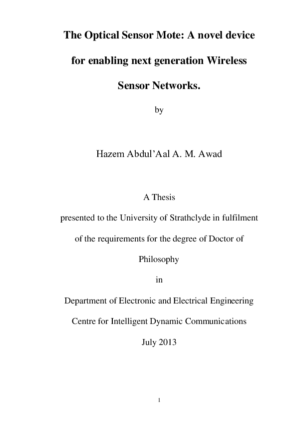
 hazem awad