Academia.edu no longer supports Internet Explorer.
To browse Academia.edu and the wider internet faster and more securely, please take a few seconds to upgrade your browser.
A High Swing Low Power CMOS Differential Voltage-Controlled Ring Oscillator
A High Swing Low Power CMOS Differential Voltage-Controlled Ring Oscillator
A High Swing Low Power CMOS Differential Voltage-Controlled Ring Oscillator
A High Swing Low Power CMOS Differential Voltage-Controlled Ring Oscillator
A High Swing Low Power CMOS Differential Voltage-Controlled Ring Oscillator
 Eric Fabris
2007
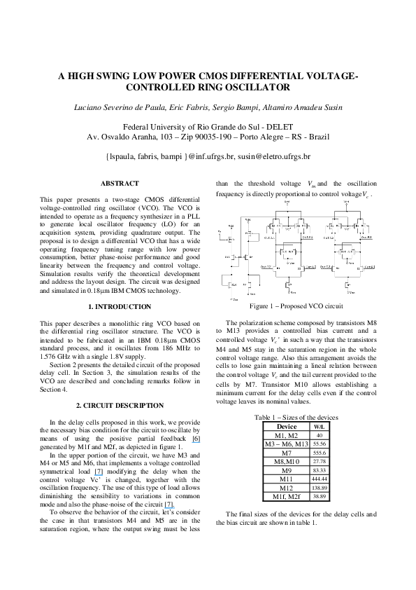
This paper presents the design of a two-stage CMOS differential voltage-controlled ring oscillator (VCO). The VCO is designed to operate as a module of the frequency synthesizer in a PLL to generate the local oscillator (LO) of a multi-band acquisition system, providing quadrature output. The goal is a wide operating frequency tuning range of 440 MHz-1.4 GHz in the VCO with low power consumption, 90 dBc/Hz @ 600 KHz phase-noise performance and good linearity between the frequency and control voltage. Simulation results verify the theoretical development as well as the final layout design. The symmetric load transistor operation region controls the frequency behavior achieved by the ring VCO, which shows a monotonic relation with the control voltage when the loads are operated in saturation. The circuit was designed, implemented and simulated in a 0.18 mum IBM CMOS technology.
Related Papers
IEEE Microwave Magazine
CMOS Differential Ring OscillatorsT he integrated dif-ferential ring oscil-l a t o r (D RO) i n c o m p l e m e n t a r y metal oxide semi-conductor (CMOS) technol-ogy has been used in numer-ous products for a long time. Its presence has been extended to high-speed clock and data recovery (CDR) circuits for opti-cal communication, analog and digitally controlled oscillators, fre-quency dividers of high-frequency synthesizers, clock generators of digi-tal circuits, analog-to-digital convert-ers (ADCs), and many more applications [1]–[5]. Implementations of these ring oscilla-tors are seen in emerging technologies such as ultrawideband (UWB) and radio frequency iden-tification (RFID) as well as wireless sensor networks (WSNs) and short-range communication devices [6], [7]. The DRO is a good design choice for integrated circuit (IC) designers because of its continued use in different bulk CMOS tech-nologies. This article presents implementation techniques and performance comparisons of the DRO as a CMOS voltage-control...
Analog Integrated Circuits and Signal Processing
A low power consumption CMOS differential-ring VCO for a wireless sensor2012 •
2008 IEEE International Conference on Semiconductor Electronics
Low-power high-tuning range CMOS ring oscillator VCOs2008 •
International Journal of Engineering Sciences & Research Technology
Wide-Band Current Starved Ring CMOS Voltage Controlled Oscillator (VCO) using 0.18 μm CMOS Technology.2014 •
This paper describes a design and implementation of Current Starved CMOS Voltage Controlled Oscillator based on Ring Oscillator. Efforts are made to design a CMOS Voltage controlled oscillator having wide frequency range with High frequency, Low power. So, the CMOS VCO designed here having a Five Stage Current Starved CMOS VCO and Seven Stage Current Starved CMOS VCO. The design is optimization and simulates on TSMC 180nm CMOS process at 1.8 V supply voltages. The Five Stage CS VCO results show that the oscillation frequency of VCO varies between 18.724MHz to 1890.4MHz and power consumption may varies between 35.39 µW to 25.013 µW and the Seven stage CS VCO results show that the oscillation frequency of VCO varies between 68.971MHz to 2099.5 MHz and power consumption may varies between 2.59 µW to 348.81 µW.
International Journal of Engineering Sciences & Research Technology
Wide-Band Single Stage Source Coupled CMOS Voltage Controlled Oscillator (VCO) using 0.18 μm CMOS Technology2014 •
This paper describes a design and implementation of Single Stage Source Coupled CMOS Voltage Controlled Oscillator based on Ring Oscillator. Efforts are made to design a CMOS Voltage controlled oscillator having wide frequency range with High frequency, Low power. So, the CMOS VCO designed here having a Single Stage Source Coupled CMOS VCO. The design is optimization and simulates on TSMC 180nm CMOS process at 1.8 V supply voltages. The results show that the oscillation frequency of VCO varies between 78.46MHz to 287.93MHz and power consumption may varies between 0.03µW to 0.86µW
This paper presents a five and three stages current starved Voltage Controlled Oscillator (CMOS VCO) for low power Phase Lock Loop (PLL). The implemented design used a standard 0.18µm CMOS Technology with simulation CAD software mentor graphics tool. uses two models of P-channel and N-channel Mosfets Model I and II. The Model I and II of P-channel. The experimental results presentented suggests that the designed exibits twoVCO frequency ranging from 21MHz to 315.34 MHz at low power. The designed circuit is simulated using 180nm SCN018 Technology, and the product of this current and voltage approximate the power consumption to be 105.3mW, the procedures of the system design are illustrated step by step in this paper. The proposed design is suitable for PLL as a frequency multiplier based on its features as presented.
A 2GHz carrier recovery Costas Loop based BPSK detector is designed using CMOS 0.18μm technology. The designed BPSK detector consists of single to differential conversion circuit, phase/frequency detector, Voltage Controlled Oscillator (VCO), differential to single conversion circuit, first order loop filter and a third multiplier. Different architectures available for each block have been discussed along with the design methodology adopted. The schematics were simulated in analog design environment. These papers present a CMOS Voltage Controlled Oscillator with high oscillation frequency and low power consumption. It also describes the performance comparison of a current starved VCO and source coupled VCO for BPSK Costas Loop Filter. The designed Costas loop for BPSK detection is able to detect and demodulate data rates up to 50Mbps. The loop can track within the VCO frequency range of 1.99GHz to 2.01GHz. The lock range achieved for this loop is 20MHz. The power consumption of the Costas Loop BPSK detector was found to be 0.25mW.
RELATED PAPERS
Microelectronics Journal
A cross coupled low phase noise oscillator using an output swing enhancement technique2014 •
Circuits, Systems, and Signal Processing
A New Transmission Gate Cascode Current Mirror Charge Pump for Fast Locking Low Noise PLL2014 •
IEEE Radio Frequency Integrated Circuits (RFIC) Symposium, 2003
A 1.8 V monolithic CMOS nested-loop frequency synthesizer for GSM receivers at 1.8 GHz2003 •
International Journal of Microwave Science and Technology
Low Phase Noise and High Conversion Gain Oscillator Mixer Constructed with a 0.18-μm CMOS Technology2009 •
… and Diagnostics of …
A Build-In Self-Test technique for RF Mixers2010 •
Progress In Electromagnetics Research C
A Q-Band Frequency Synthesizer in 0.13 Μm Sige Bicmos2014 •
Circuits and Systems
Voltage Controlled Ring Oscillator Design with Novel 3 Transistors XNOR/XOR Gates2011 •
2010 •
IEEE Journal of Solid-State Circuits
Differential CMOS circuits for 622-MHz/933-MHz clock and data recovery applications2000 •
2014 International Conference on Information Science, Electronics and Electrical Engineering
Multi-phase ring oscillator with minimized phase noise for ultra-wideband applications2014 •
Micro and Nanosystems
Advances in Active Inductor Based CMOS Band-Pass Filter2018 •
Journal of Circuits, Systems, and Computers
A High-Speed Temperature Sensor with Low Supply Sensitivity for SoC Thermal Monitoring2018 •
WSEAS Transactions on Electronics
Optimizing LC VCO Performances Through a Heuristic2011 18th IEEE International Conference on Electronics, Circuits, and Systems
A 60-GHz quadrature PLL in 90nm CMOS2011 •
2007 •
Journal of Electronic Testing
A Design for Testability Scheme for CMOS LC-Tank Voltage Controlled Oscillators2000 •
2008 •
2014 •
International Journal of …
A new temperature compensation method for a 2.5 GHz integrated VCO2007 •